 | –≠–ª–µ–∫—Ç—Ä–æ–Ω–Ω—ã–π –∫–æ–º–ø–æ–Ω–µ–Ω—Ç: SII141 | –°–∫–∞—á–∞—Ç—å:  PDF PDF  ZIP ZIP |
Subject to Change without Notice
Si
I
141
PanelLink
Æ
Digital Receiver
July
1999
General Description
Features
The Si
I
141 uses PanelLink Digital technology to support displays ranging
from VGA to High Refresh XGA (25-86 MHz), which is ideal for LCD desktop
monitor applications. With a flexible single or dual pixel out interface and
selectable output drive, the Si
I
141 receiver supports up to true color panels (24
bit/pixel, 16.7M colors) in 1 pixel/clock mode (18 bit/pixel in 2 pixel/clock mode).
PanelLink also features an inter-pair skew tolerance up to 1 full input clock cycle
and a highly jitter tolerant PLL design. Since all PanelLink products are
designed on scaleable CMOS architecture to support future performance
requirements while maintaining the same logical interface, system designers can
be assured that the interface will be fixed through a number of technology and
performance generations.
PanelLink Digital technology simplifies PC design by resolving many of the
system level issues associated with high-speed digital design, providing the
system designer with a digital interface solution that is quicker to market and
lower in cost.
∑
Scaleable Bandwidth: 25-86 MHz (VGA to High Refresh
XGA)
∑
Low Power: 3.3V core operation & power-down mode
∑
High Skew Tolerance: 1 full input clock cycle (15ns at 65
MHz)
∑
Pin-compatible with Si
I
101
∑
Sync Detect: for Plug & Display "Hot Plugging"
∑
Cable Distance Support: over 5m with twisted-pair, fiber-
optics ready
∑
Compliant with DVI 1.0 (DVI is backwards compatible
with VESAÆ P&D
TM
and DFP)
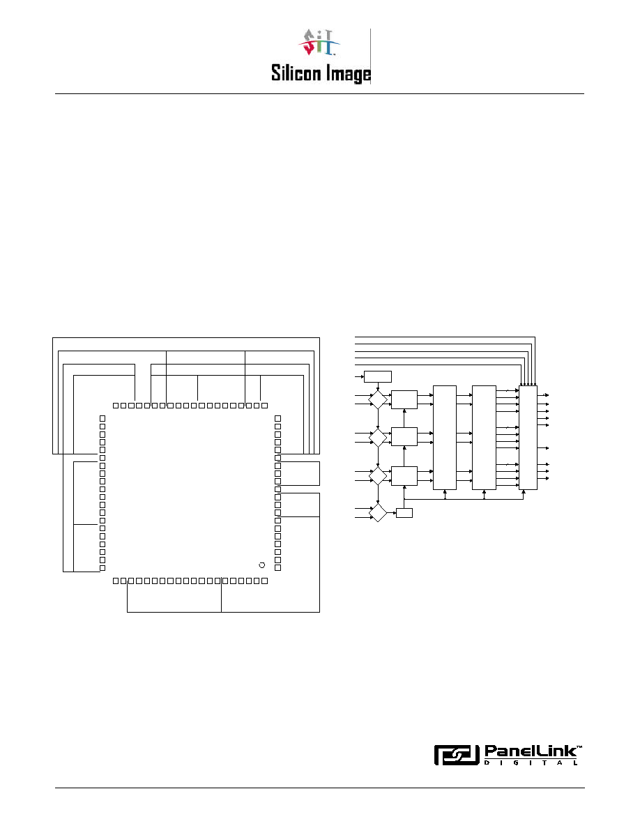
Si
I
141 Pin Diagram
Functional Block Diagram
INTER-
CHANNEL
SYNC.
DECODER
CLT3
CLT2
DE2
CLT1
PLL_SYNC
DE1
VSYNC
HSYNC
DE0
8
8
8
VCR
Termination
Control
EXT_RES
PANEL
INTER-
FACE
LOGIC
Q[35:0/23:0]
ODCK
DE
HSYNC
VSYNC
CLT1
CLT2
CLT3
RX2+
RX2-
RX1+
RX1-
RX0+
RX0-
RXC+
RXC-
PIXS
OCK_INV
PLL
24/36
VCR
VCR
VCR
DFO
ST
SCDT
PDO
DATA
RECOVERY
CH2
DATA
RECOVERY
CH0
DATA
RECOVERY
CH1
1
SiI141
80-Pin TQFP
(Top View)
PD
2
PDO
3
OGND
4
PIXS
5
DFO
6
SCDT
7
CTL1
8
CTL2
9
CTL3
10
GND
11
HSYNC
12
OGND
13
VSYNC
14
OVCC
15
Q0
16
Q5
21
Q6
22
Q7
23
Q8
24
Q9
25
OGND
26
Q10
27
OVCC
28
Q11
29
Q12
30
Q13
31
Q14
32
Q15
33
Q16
34
Q17
35
56
Q30
55
Q29
54
Q28
53
Q27
52
Q26
51
VCC
50
Q25
49
OVCC
48
Q24
47
OGND
46
Q23
45
Q22
44
Q21
43
Q20
42
DE
41
Q31
OCK_INV
80
ST
79
PGND
78
PVCC
77
EXT_RES
76
RESERVED
75
RXC+
74
RXC-
73
AGND
72
RX0-
71
RX0+
70
AVCC
69
RX1-
68
RX1+
67
AGND
66
RX2-
65
8-bit Channel 0 Data
1-pixel/clock
24-bit Input Data for 1-pixel/clock mode
DIFFERENTIAL SIGNAL
ODCK
36
8-bit Channel 1 Data
1-pixel/clock
MISC.
GENERAL
PURPOSE
CONTROL
CONTROL
Q1
17
Q2
18
Q3
19
Q4
20
GND
37
Q18
38
VCC
39
Q19
40
60
Q34
59
Q33
58
Q32
57
Q35
RX2+
64
AVCC
63
GND
62
VCC
61
8-bit Channel 2 Data
1-pixel/clock
6-bit Even Channel 0
Data 2-pixel/clock
6-bit Even Channel 2
Data 2-pixel/clock
6-bit Even Channel 1
Data 2-pixel/clock
6-bit Odd Channel 0
Data 2-pixel/clock
6-bit Odd Channel 1
Data 2-pixel/clock
6-bit Odd Channel 2
Data 2-pixel/clock
18-bit Even Data for 2-pixel/clock mode
18-bit Odd Data for 2-pixel/clock mode
RESERVED

Silicon Image, Inc.
SiI141
SiI/DS-0004-D
2
Subject to Change without Notice
Absolute Maximum Conditions
Note:
Permanent device damage may occur if absolute maximum conditions are exceeded.
Functional operation should be restricted to the conditions described under Normal Operating Conditions.
Symbol
Parameter
Min
Max
Units
V
CC
Supply Voltage 3.3V
-0.3
4.0
V
V
I
Input Voltage
-0.3
V
CC
+ 0.3
V
V
O
Output Voltage
-0.3
V
CC
+ 0.3
V
T
A
Ambient Temperature (with power applied)
-25
105
∞
C
T
STG
Storage Temperature
-40
125
∞
C
P
PD
Package Power Dissipation
1
W
Normal Operating Conditions
Symbol
Parameter
Min
Typ
Max
Units
V
CC
Supply Voltage
3.00
3.3
3.6
V
V
CCN
Supply Voltage Noise
100
mV
P-P
T
A
Ambient Temperature (with power applied)
0
25
70
∞
C
Note:
1
Guaranteed by design.
DC Digital I/O Specifications
Under normal operating conditions unless otherwise specified.
Symbol
Parameter
Conditions
Min
Typ
Max
Units
V
IH
High-level Input Voltage
2
V
V
IL
Low-level Input Voltage
0.8
V
V
OH
High-level Output Voltage
2.4
V
V
OL
Low-level Output Voltage
0.4
V
V
CINL
Input Clamp Voltage
1
I
CL
= -18mA
GND -0.8
V
V
CIPL
Input Clamp Voltage
1
I
CL
= 18mA
IVCC + 0.8
V
V
CONL
Output Clamp Voltage
1
I
CL
= -18mA
GND -0.8
V
V
COPL
Output Clamp Voltage
1
I
CL
= 18mA
OVCC + 0.8
V
I
IL
Input Leakage Current
-10
10
µ
A
Note:
1
Guaranteed by design.
DC Specifications
Under normal operating conditions unless otherwise specified. Low drive strength values, when ST=0, are shown in brackets.
Symbol
Parameter
Conditions
Min
Typ
Max
Units
I
OHD
Output High Drive
Data and Controls
V
OUT
= V
OH
ST=1
ST=0
5.0
2.51
10.3
5.15
17.6
8.8
mA
I
OLD
Output Low Drive
Data and Controls
V
OUT
= V
OL
ST=1
ST=0
-5.5
-2.8
-8.3
-4.2
-11.2
-5.6
mA
I
OHC
ODCK High Drive
V
OUT
= V
OH
ST=1
ST=0
10.1
5.0
20.6
10.3
35.1
17.6
mA
I
OLC
ODCK Low Drive
V
OUT
= V
OL
ST=1
ST=0
-11.1
-5.5
-16.7
-8.3
-22.4
-11.2
mA
V
ID
Differential Input Voltage
Single Ended Amplitude
75
1000
mV
I
PD
Power-down Current
1
25
µ
A
I
PDL
Output leakage current to ground in
high impedance mode (PD, PDO =
LOW)
10
uA
I
CCR
Receiver Supply Current
DCLK=86MHz, 1-pixel/clock mode
2
C
LOAD
= 10pF
R
EXT_SWING
= 680
Typical Pattern
3
157
182
mA
DCLK=86MHz, 1-pixel/clock mode
2
C
LOAD
= 10pF
R
EXT_SWING
= 680
Worst Case Pattern
4
172
194
mA
Notes:
1
The transmitter must be in power-down mode, powered off, or disconnected for the current to be under this maximum.
2
For worst case I/O power consumption.
3
The Typical Pattern contains a gray scale area, checkerboard area, and text.
4
Black and white checkerboard pattern, each checker is one pixel wide.

Silicon Image, Inc.
SiI141
SiI/DS-0004-D
3
Subject to Change without Notice
AC Specifications
Under normal operating conditions unless otherwise specified. Low drive strength values, when ST=0, are given below.
Symbol
Parameter
Conditions
Min
Typ
Max
Units
T
DPS
Intra-Pair (+ to -) Differential Input Skew
86 MHz
One pixel / clock
470
ps
T
CCS
Channel to Channel Differential Input Skew
86 MHz
One pixel / clock
7
ns
T
IJIT
Worst Case Differential Input Clock Jitter tolerance
1,2
65 MHz, One Pixel / Clock
465
ps
86 MHz, One Pixel / Clock
350
ps
D
LHT
Low-to-High Transition Time: Data and Controls
C
L
= 10pF, ST=1
C
L
= 5pF, ST=0
5.2
4.4
ns
ODCK
C
L
= 10pF, ST=1
C
L
= 5pF, ST=0
2.3
1.8
ns
D
HLT
High-to-Low Transition Time: Data and Controls
C
L
= 10pF, ST=1
C
L
= 5pF, ST=0
3.8
3
ns
ODCK
C
L
= 10pF, ST=1
C
L
= 5pF, ST=0
2
1.5
ns
T
SOF
Data/Control Setup Time to ODCK falling
4
(OCK_INV=0):
65 MHz, One Pixel / Clock, PIXS = 0
C
L
= 10pF, ST=1
C
L
= 5pF, ST=0
2
1.6
ns
43 MHz, Two Pixel / Clock, PIXS = 1
C
L
= 10pF, ST=1
C
L
= 5pF, ST=0
5
5
ns
T
HOF
Data/Control Hold Time to ODCK falling
4
(OCK_INV=0):
65 MHz, One Pixel / Clock, PIXS = 0
C
L
= 10pF, ST=1
C
L
= 5pF, ST=0
6
6
ns
43 MHz, Two Pixel / Clock, PIXS = 1
C
L
= 10pF, ST=1
C
L
= 5pF, ST=0
12
12
ns
R
CIP
ODCK Cycle Time (1 pixel/clock)
11.6
50
ns
F
CIP
ODCK Frequency (1 pixel/clock)
20
86
MHz
R
CIP
ODCK Cycle Time (2 pixels/clock)
23.3
100
ns
F
CIP
ODCK Frequency (2 pixels/clock)
10
43
MHz
R
CIH
ODCK High Time
65 MHz, One Pixel / Clock, PIXS = 0
3
C
L
= 10pF, ST=1
C
L
= 5pF, ST=0
5
4.4
ns
43 MHz, Two Pixel / Clock, PIXS = 1
3
C
L
= 10pF, ST=1
C
L
= 5pF, ST=0
9
8.2
ns
R
CIL
ODCK Low Time
65 MHz, One Pixel / Clock, PIXS = 0
3
C
L
= 10pF, ST=1
C
L
= 5pF, ST=0
6
5
ns
43 MHz, Two Pixel / Clock, PIXS = 1
3
C
L
= 10pF, ST=1
C
L
= 5pF, ST=0
9
9
ns
T
HSC
Link disabled (DE inactive) to SCDT low
1
160
ms
Link disabled (Tx power down) to SCDT low
5
200
250
ms
T
FSC
Link enabled (DE active) to SCDT high
40
Falling DE
edges
T
PDL
Delay from PD/ PDO Low to high impedance outputs
8
ns
Notes:
1
Jitter defined as per DVI 1.0 Specification, Section 4.6 Jitter Specification.
2
Jitter measured with Clock Recovery Unit as per DVI 1.0 Specification, Section 4.7 Electrical Measurement Procedures.
3
Output clock duty cycle is independent of the differential input clock duty cycle and the IDCK duty cycle.
4
The setup and hold timing for the data and controls relative to the ODCK rising edge (OCK_INV=1) is by design the same
as the falling edge timing.
5
Measured when transmitter was powered down (see Si
I
/AN-0005 "PanelLink Basic Design /Application Guide," Section 2.4).
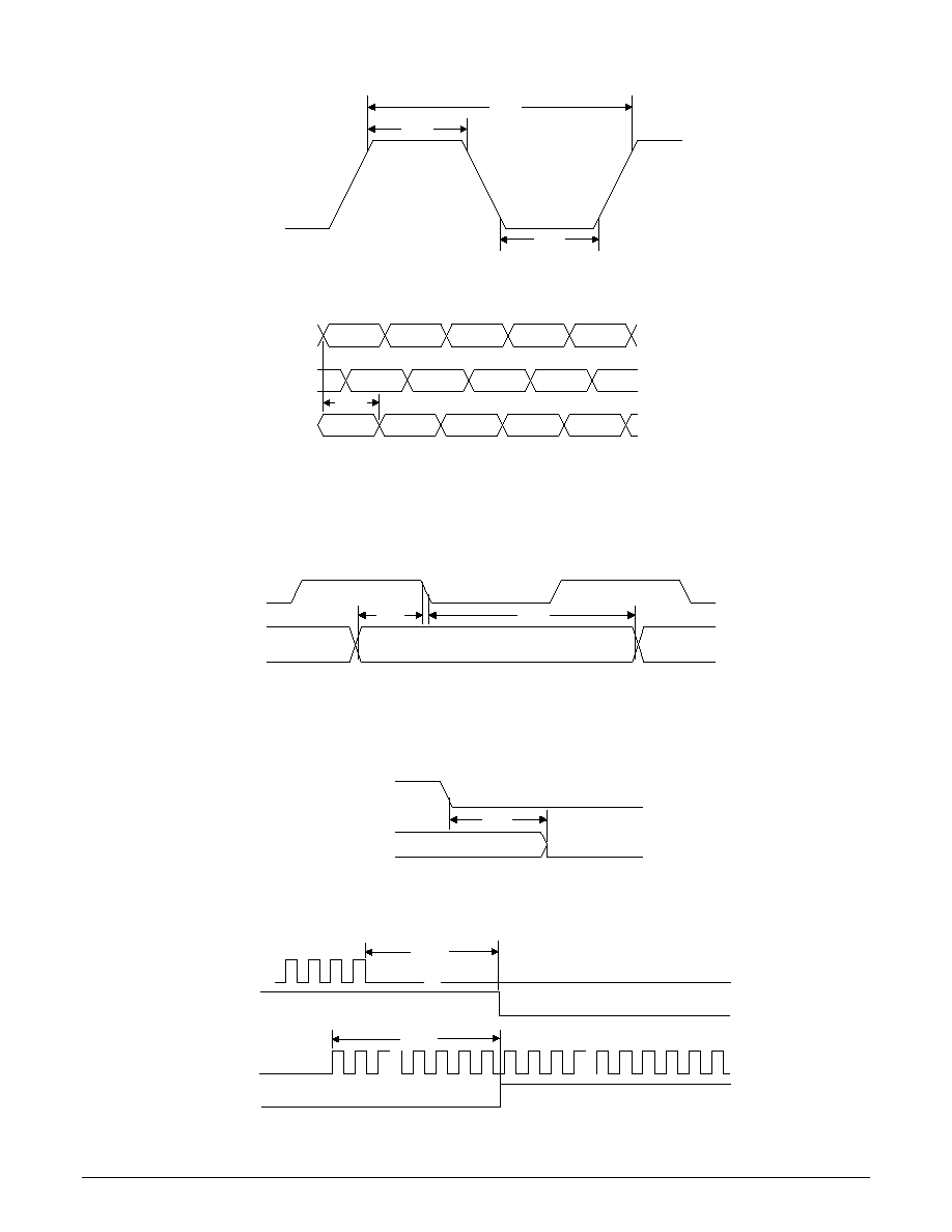
Timing Diagrams
Figure 1. Digital Output Transition Times
10pF (5pF)
SiI141
D
LHT
D
HLT
80%
80%
20%
20%
Silicon Image, Inc.
SiI141
SiI/DS-0004-D
4
Subject to Change without Notice
Figure 2. Receiver Clock Cycle/High/Low Times
Figure 3. Channel-to-Channel Skew Timing
Output Timing
Figure 4. Output Data Setup/Hold Times to ODCK
Figure 5. Output Signals Disabled Timing from PD Active
Figure 6. SCDT Timing from DE Inactive/Active
R
CIH
R
CIL
R
CIP
V
IH
V
IH
V
IL
V
IL
RX0
RX1
RX2
T
CCS
V
DIFF=0V
V
DIFF=0V
Q[35:0],
VSYNC,
HSYNC,
CTL[3:1]
DE
ODCK
T
SOF
T
HOF
V
OL
V
OL
V
OH
V
OL
V
OH
V
OH
PD
T
PDL
Q[35:0],DE,
VSYNC,HSYNC,
CTL[3:1]
V
IL
DE
SCDT
DE
SCDT
T
HSC
T
FSC
Silicon Image, Inc.
SiI141
SiI/DS-0004-D
5
Subject to Change without Notice
Output Pin Description
Pin Name
Pin #
Type
Description
Q35 ≠ Q0
See
Out
Output Data [35:0].
Si
I
141
Output data is synchronized with output data clock (ODCK).
Pin
When PIXS is low Q35-Q24 are low and Q23-Q0 output 24-bit/pixel data.
Diagram
When PIXS is high Q17-Q0 output the even numbered pixels (pixel 0, 2, 4, ... , etc.) and Q35-Q18 output the
odd numbered pixels (pixel 1, 3, 5, ... , etc.).
Refer to the TFT Signal Mapping (Si
I
/AN-0008) and DSTN Signal Mapping (Si
I
/AN-0007) application notes
which tabulate the relationship between the input data to the transmitter and output data from the receiver.
A low level on PD or PDO will put the output drivers into a high impedance (tri-state) mode. A weak internal
pull-down device brings each output to ground.
ODCK
36
Out
Output Data Clock.
A low level on PD or PDO will put the output drivers into a high impedance (tri-state) mode. A weak internal
pull-down device brings each output to ground.
DE
41
Out
Output Data Enable.
A low level on PD or PDO will put the output drivers into a high impedance (tri-state) mode. A weak internal
pull-down device brings each output to ground.
HSYNC
12
Out
Horizontal Sync output control signal.
VSYNC
14
Out
Vertical Sync output control signal.
CTL1
8
Out
General output control signal 1. This pin is not controlled by PDO.
CTL2
9
Out
General output control signal 2
CTL3
10
Out
General output control signal 3.
A low level on PD or PDO will put the output drivers into a high impedance (tri-state) mode. A weak internal
pull-down device brings each output to ground.
Configuration Pin Description
Pin Name
Pin #
Type
Description
OCK_INV
80
In
ODCK Polarity. A low level selects normal ODCK output, which enables data latching on the falling edge. A high
level (3.3V) selects inverted ODCK output, which enables data latching on the rising edge. Both conditions are for
color TFT panel support. For color 24-bit DSTN panel support, please refer to the DSTN Signal Mapping
(Si
I
/AN-0008-A) application note.
PIXS
5
In
Pixel Select. A low level indicates that output data is one pixel (up to 24-bit) per clock and a high level (3.3V)
indicates that output data is two pixels (up to 36-bit) per clock.
DF0
6
In
Output Data Format. This pin controls clock and data output format. A low level indicates that ODCK runs
continuously for color TFT panel support and a high level (3.3V) indicates that ODCK is stopped (LOW) for color
24-bit DSTN panel support when DE is low. Refer to the TFT Signal Mapping (Si
I
/AN-0007-A) and DSTN
Signal Mapping (Si
I
/AN-0008-A) application notes for a table on TFT or DSTN panel support.
ST
79
In
Output Driver Strength. A low level indicates low drive. A high level indicates high drive.
Power Management Pin Description
Pin Name
Pin #
Type
Description
SCDT
7
Out
SyncDetect. A high level is output when DE is toggling. A low level is output when DE is inactive.
PD
2
In
Power Down (active low). A high level (3.3V) indicates normal operation and a low level indicates power down
mode. During power down mode all internal circuitry is powered down and digital I/O are set the same as when
PDO is asserted. (see PDO pin description).
PDO
3
In
Power Down Output (active low). A high level indicates normal operation. A low level puts the output drivers only into
a high impedance (tri-state) mode. A weak internal pull-down device brings each output to ground. There is an
internal pull-up resistor on PDO that defaults the chip to normal operation if left unconnected. SCDT and CTL1 are
not tri-stated by this pin.
Differential Signal Data Pin Description
Pin Name
Pin #
Type
Description
RX0+
70
Analog
TMDS Low Voltage Differential Signal input data pairs.
RX0-
71
RX1+
67
RX1-
68
RX2+
64
RX2-
65
RXC+
74
Analog
TMDS Low Voltage Differential Signal input clock pair.
RXC-
73
EXT_RES
76
Analog
Impedance Matching Control. Resistor value should be ten times the characteristic impedance of the cable. In the
common case of 50
transmission line, an external 500
resistor must be connected between AVCC and this
pin.