 | –≠–ª–µ–∫—Ç—Ä–æ–Ω–Ω—ã–π –∫–æ–º–ø–æ–Ω–µ–Ω—Ç: SII154 | –°–∫–∞—á–∞—Ç—å:  PDF PDF  ZIP ZIP |

Si
I
154
Preliminary Data Sheet
General Description
The SiI154 transmitter uses PanelLink
Æ
Digital
technology to support displays ranging from VGA to
SXGA resolutions (25-112MPps) in a single link
interface. The SiI154 transmitter has a highly flexible
interface with 12-bit (Ω pixel) or 24-bit 1 pixel/clock
input for true color (16.7 million) support. In 24-bit
mode, the data may be latched on the positive or
negative edge of the clock. In 12-bit mode, multiple
clocking options exist: with a single clock, data will be
clocked on the falling and the rising edge; with dual
clocks data can be clocked on either the falling edge
of the rising edge of both clocks.
PanelLink Digital technology simplifies PC design by
resolving many of the system level issues associated
with high-speed digital design, providing the system
designer with a digital interface solution that is
quicker to market and lower in cost.
Features
∑
Scaleable Bandwidth: 25-112 Mega-pixels/sec
(VGA to SXGA)
∑
Flexible Panel Interface: 12-bit (Ω pixel) or 24-bit 1
pixel/clock inputs
∑
I
2
C Slave Programming Interface
∑
Low Voltage Interface: 1.0 to 1.8V capable
∑
Receiver Detection: Supports Hot Plug Detection
through RxDetect feature
∑
De-skewing Option: varies clock to data timing
∑
High Inter-Pair Skew Tolerance: 1 full input clock
cycle (9 ns at 108MHz)
∑
Low Power: 3.3V core operation and power down
mode
∑
Cable Distance Support: over 5m with twisted
pair, fiber-optics ready
∑
Standards Compliant with DVI 1.0 (DVI is
backwards compliant with VESA
Æ
P&D
TM
and
DFP)
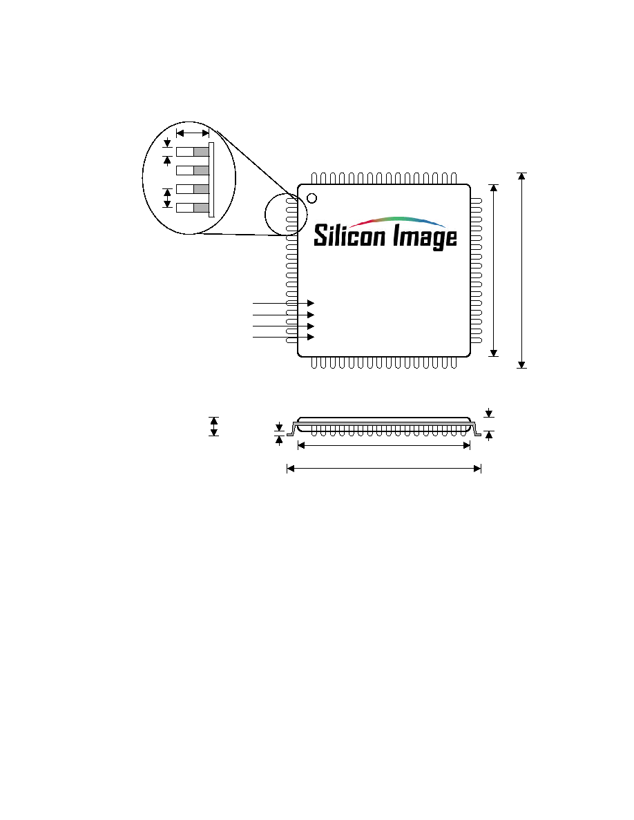
SiI 154 Pin Diagram
VCC
DE
VREF
HSYNC
VSYNC
CTL3/A3/DK3
CTL2/A2/DK2
CTL1/A1/DK1
EDGE/HTPLG
PD
MSEN
VCC
ISEL/RST
DSEL/SDA
BSEL/SCL
GND
PGND
PVCC1
EXT_SWING
AGND
TXC-
TXC+
AVCC
TX0-
TX0+
AGND
TX1-
TX1+
AVCC
TX2-
TX2+
VCC
RESERVED
DKEN
D23
D22
D21
D20
D19
D18
D17
D16
D15
D14
D13
D12
GND
PVCC2
D11
D10
D9
D8
D7
D6
IDCK-
IDCK+
D5
D4
D3
D2
D1
D0
GND
1
2
3
4
5
6
7
8
9
10
11
12
13
14
15
16
17
18
19
20
21
22
23
24
25
26
27
28
29
30
31
32
33
34
35
36
37
38
39
40
41
42
43
44
45
46
47
48
49
50
51
52
53
54
55
56
57
58
59
60
61
62
63
64
SiI 154
64-Pin TQFP
(Top View)
AGND
Figure 1. Si
I
154 Pin Diagram
Silicon Image, Inc.
Si
I
154
Si
I
/DS-0010-D
Revision 0.94
Subject to Change without Notice
2
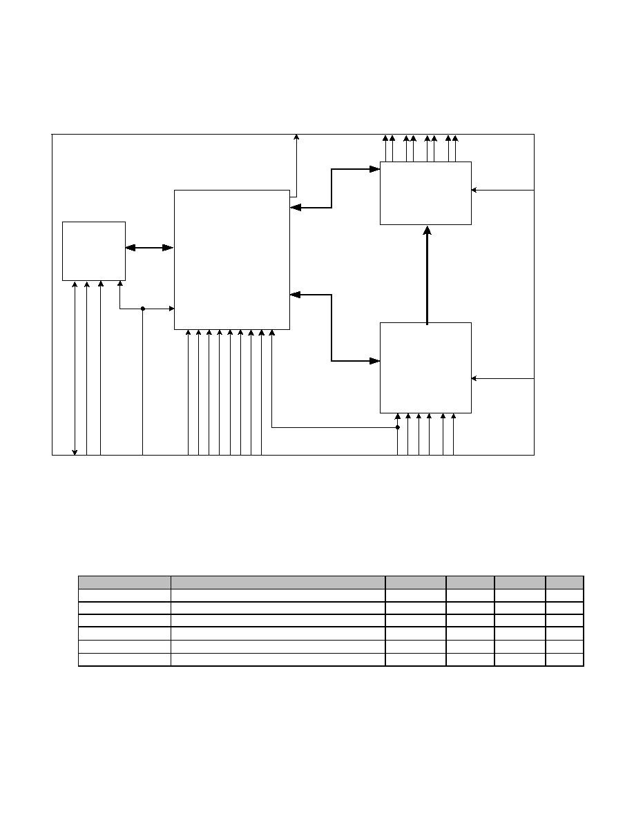
Functional Block Diagram
Electrical Specifications
Absolute Maximum Conditions
Symbol
Parameter
Min
Typ
Max
Units
V
CC
Supply Voltage 3.3V
-0.3
4.0
V
V
I
Input Voltage
-0.3
V
CC
+ 0.3
V
V
O
Output Voltage
-0.3
V
CC
+ 0.3
V
T
A
Ambient Temperature (with power applied)
-25
105
∞
C
T
STG
Storage Temperature
-40
125
∞
C
P
PD
Package Power Dissipation
1
W
Notes:
1
Permanent device damage may occur if absolute maximum conditions are exceeded.
2
Functional operation should be restricted to the conditions described under Normal Operating Conditions.
Registers
&
Configuration
Logic Block
SCL
SDA
HTPLG
PD
EDGE
BSEL
DSEL
A[3:1]
I
2
C
Slave
Machine
Data Capture
Logic Block
D[23:0]
IDCK+
IDCK-
VSYNC
HSYNC
CTL[3:1]
TXC+
TX0+
TX1+
TX2+
VREF
DE
MSEN
PanelLink
Digital
core
ISEL/RST
EXT_RES
DK[3:1]
DKEN
TXC-
TX0+
TX1+
TX2+
Silicon Image, Inc.
Si
I
154
Si
I
/DS-0010-D
Revision 0.94
Subject to Change without Notice
3
Normal Operating Conditions
Symbol
Parameter
Min
Typ
Max
Units
V
CC
Supply Voltage
3.0
3.3
3.6
V
V
CCN
Supply Voltage Noise
1
100
mV
P-P
T
A
Ambient Temperature (with power applied)
0
25
70
∞
C
Notes:
1
Guaranteed by design.
DC Digital I/O Specifications
Under normal operating conditions unless otherwise specified.
Symbol
Parameter
Conditions
Min
Typ
Max
Units
V
IH
High Swing High-level Input
Voltage
V
REF =
V
CC
2
V
V
IL
High Swing Low-level Input
Voltage
V
REF =
V
CC
0.8
V
V
DDQ
2
Low Swing Voltage
1
1.8
V
V
SH
Low Swing High-level Input
Voltage
V
REF =
V
DDQ
/2
V
DDQ
/2 +
300mV
V
V
SL
Low Swing Low-level Input
Voltage
V
REF =
V
DDQ
/2
V
DDQ
/2 ≠
100mV
V
V
CINL
Input Clamp Voltage
1
I
CL
= -18mA
GND -0.8
V
V
CIPL
Input Clamp Voltage
1
I
CL
= 18mA
VCC + 0.8
V
I
IL
Input Leakage Current
-10
10
µ
A
Notes:
1
Guaranteed by design.
2
V
DDQ
Defines max voltage level of low swing input. It is not an actual input voltage.
DC Specifications
Under normal operating conditions unless otherwise specified.
Symbol
Parameter
Conditions
Min
Typ
Max
Units
V
OD
Differential Voltage
R
LOAD
= 50
Single ended peak to peak
amplitude
R
EXT_SWING
= 850
250
300
350
mV
R
EXT_SWING
= 680
310
370
430
mV
R
EXT_SWING
= 400
580
650
720
mV
V
DOH
Differential High-level Output
Voltage
1
AVCC
V
V
REF
Input Reference Voltage
Low Swing
0.45
V
DDQ
/2
1
V
High Swing
VCC
V
I
DOS
Differential Output Short Circuit
Current
1
V
OUT
= 0V
5
µ
A
I
PD
Power-down Current
2
4
mA
I
CCT
Transmitter Supply Current
DCLK = 112 MHz,
1 pixel/clock mode,
R
EXT_SWING
= 680
Worse Case Pattern
3
68
90
mA
Notes:
1
Guaranteed by design.
2
Assumes all inputs to the transmitter are not toggling.
3
Black and white checkerboard pattern, each checker is one pixel wide.
Silicon Image, Inc.
Si
I
154
Si
I
/DS-0010-D
Revision 0.94
Subject to Change without Notice
4
AC Specifications
Under normal operating conditions unless otherwise specified.
Symbol
Parameter
Conditions
Min
Typ
Max
Units
T
CIP
IDCK Period, 1-pixel/clock
8.93
50
ns
F
CIP
IDCK Frequency, 1-pixel/clock
20
112
MHz
T
CIH
IDCK High Time at 112MHz
3
ns
T
CIL
IDCK Low Time at 112MHz
3
ns
T
IJIT
Worst Case IDCK Clock Jitter
2,3
2
ns
T
SIDF
Data, DE
Setup Time to IDCK falling edge
(VSYNC and HSYNC are clocked on the
rising edge with equal setup and hold times)
Single Edge
(DSEL = 0, DKEN = 0,
EDGE = 0)
1.5
ns
T
HIDF
Data, DE, VSYNC, HSYNC
Hold Time from IDCK falling edge
(VSYNC and HSYNC are clocked on the
rising edge with equal setup and hold times)
Single Edge
(DSEL = 0, DKEN = 0,
EDGE = 0)
0.9
ns
T
SIDR
Data, DE, VSYNC, HSYNC
Setup Time to IDCK rising edge
1
(VSYNC and HSYNC are clocked on the
falling edge with equal setup and hold times)
Single Edge
(DSEL = 0, DKEN = 0,
EDGE = 1)
1.5
ns
T
HIDR
Data, DE, VSYNC, HSYNC
Hold Time from IDCK rising edge
1
(VSYNC and HSYNC are clocked on the
falling edge with equal setup and hold times)
Single Edge
(DSEL = 0, DKEN = 0,
EDGE = 1)
0.9
ns
T
SID
Data
Setup Time to IDCK falling/rising
edge
1
(VSYNC and HSYNC are clocked on the
secondary edge with equal setup and hold
times)
Dual Edge
(DSEL = 1, DKEN = 0,
BSEL = 0)
0.6
ns
T
HID
Data
Hold Time from IDCK falling/rising
edge
1
(VSYNC and HSYNC are clocked on the
secondary edge with equal setup and hold
times)
Dual Edge
(DSEL = 1, DKEN = 0,
BSEL = 0)
1.5
ns
T
DDF
VSYNC, HSYNC Delay from DE
falling edge
1
1 T
CIP
ns
T
DDR
VSYNC, HSYNC Delay to DE rising
edge
1
1 T
CIP
ns
T
HDE
DE high time
1
8000
T
CIP
ns
T
LDE
DE low time
1
10
T
CIP
ns
T
STEP
De-skew step size increment
DKEN = 1
240
ps
S
LHT
Differential Swing Low-to-High
Transition Time
C
LOAD
= 5pF, R
LOAD
=
50
R
EXT_SWING
= 680
0.3
0.5
0.7
ns
S
HLT
Differential Swing High-to-Low
Transition Time
C
LOAD
= 5pF, R
LOAD
=
50
R
EXT_SWING
= 680
0.3
0.5
0.7
ns
Notes:
1
Guaranteed by design.
2
Jitter can be estimated by 1) triggering a digital scope at the rising of input clock and 2) measuring the peak to
peak time spread of the rising edge of the input clock 1
u
s after the trigger.
3
Actual jitter tolerance may be higher depending on the frequency of the jitter.
Silicon Image, Inc.
Si
I
154
Si
I
/DS-0010-D
Revision 0.94
Subject to Change without Notice
5
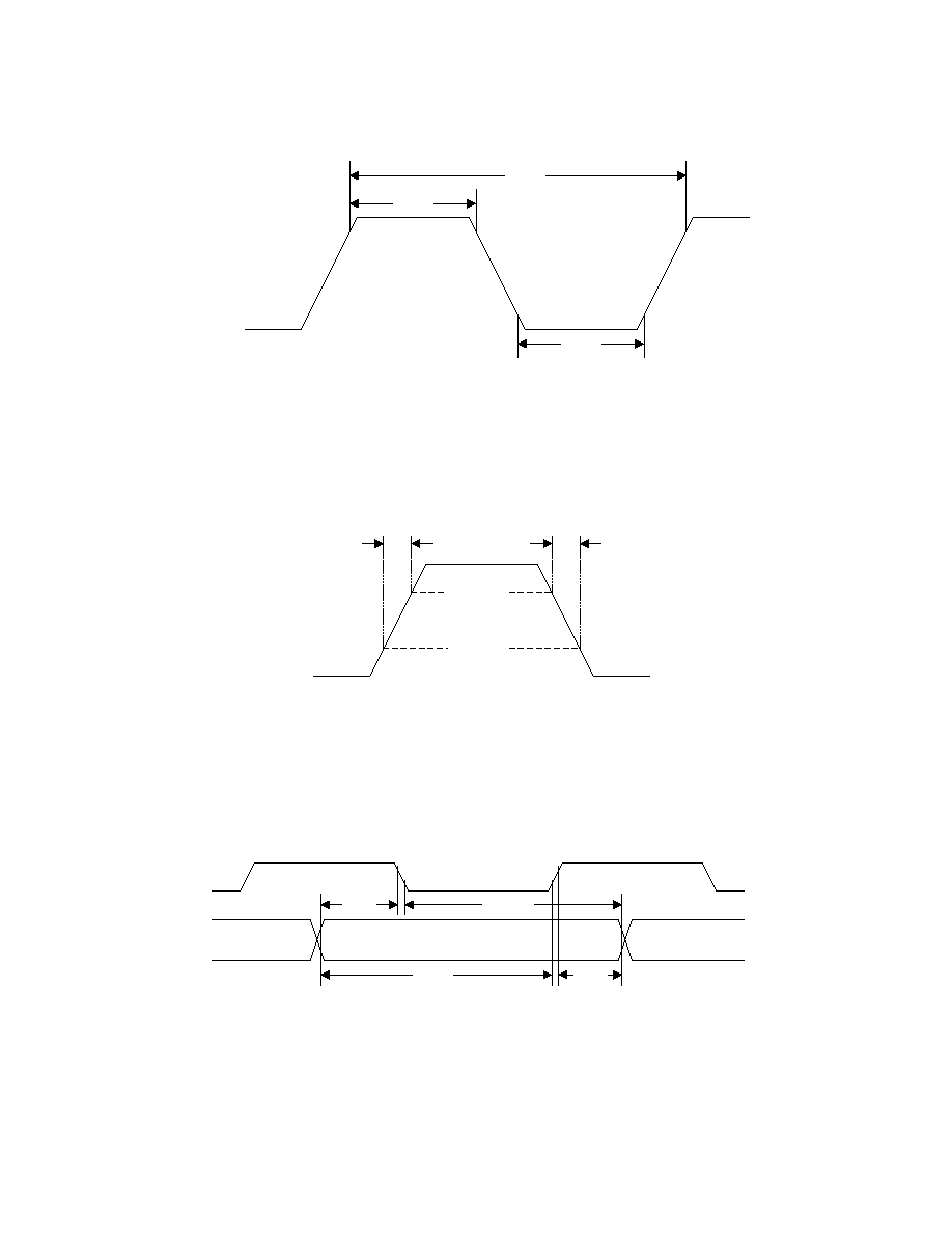
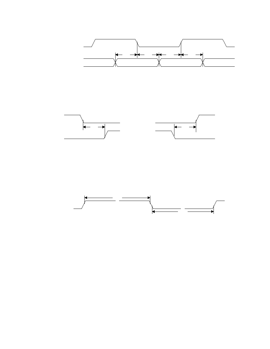
Input Timing Diagrams
T
CIH
T
CIL
T
CIP
V
IH
V
IH
V
IL
V
IL
Figure 2. Clock Cycle/High/Low Times
Figure 3. Differential Transition Times
Figure 4. Control and Single-Edge-Data Setup/Hold Times to IDCK+/IDCK-
S
LHT
20% V
OD
80% V
OD
S
HLT
D[23:0], DE,
HSYNC,VSYNC,
IDCK+/IDCK-
T
SIDF
T
HIDF
T
SIDR
T
HIDR
V
IL
V
IL
V
IH
V
IL
V
IH
V
IH
V
IH
V
IL
Silicon Image, Inc.
Si
I
154
Si
I
/DS-0010-D
Revision 0.94
Subject to Change without Notice
6
D[11:0]
IDCK+
T
SID
T
HID
T
SID
T
HID
Figure 5. Dual Edge Data Setup/Hold Times to IDCK+
Figure 6. VSYNC, HSYNC Delay Times from/to DE
DE
T
LDE
T
HDE
V
IL
V
IH
V
IL
V
IH
Figure 7. DE High/Low Times
T
DDR
T
DDF
DE
VSYNC, HSYNC
V
IL
V
IL
V
IL
V
IL
DE
VSYNC, HSYNC
Silicon Image, Inc.
Si
I
154
Si
I
/DS-0010-D
Revision 0.94
Subject to Change without Notice
7
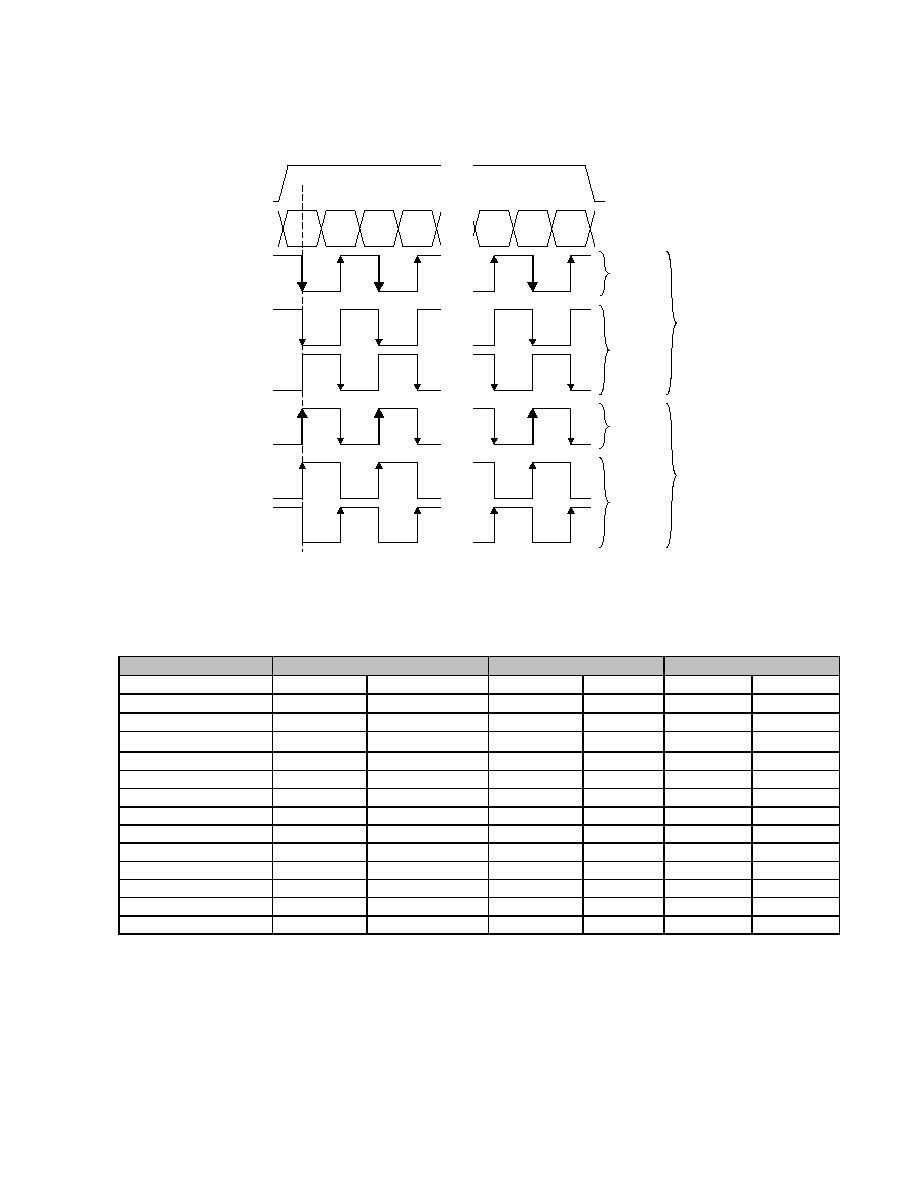
Data Mapping
12-bit Input Mode (BSEL = 0)
P
0
L
P
O
H
IDCK+
D[11:0]
P
1
L
P
1
H
P
N-1
H
P
N
L
P
N
H
DE
IDCK+
IDCK-
IDCK+
IDCK+
IDCK-
DSEL = 1
DSEL = 0
DSEL = 1
DSEL = 0
EDGE = 1
EDGE = 0
L = Low half pixel
H = High half pixel
First Latch Edge
Figure 8. Logical Interface Options for 12-bit Mode
12-bit Mode Data Mapping
P0
P1
P2
P0L
P0H
P1L
P1H
P2L
P2H
Pin Name
Low
High
Low
High
Low
High
D11
G0[3]
R0[7]
G1[3]
R1[7]
G2[3]
R2[7]
D10
G0[2]
R0[6]
G1[2]
R1[6]
G2[2]
R2[6]
D9
G0[1]
R0[5]
G1[1]
R1[5]
G2[1]
R2[5]
D8
G0[0]
R0[4]
G1[0]
R1[4]
G2[0]
R2[4]
D7
B0[7]
R0[3]
B1[7]
R1[3]
B2[7]
R2[3]
D6
B0[6]
R0[2]
B1[6]
R1[2]
B2[6]
R2[2]
D5
B0[5]
R0[1]
B1[5]
R1[1]
B2[5]
R2[1]
D4
B0[4]
R0[0]
B1[4]
R1[0]
B2[4]
R2[0]
D3
B0[3]
G0[7]
B1[3]
G1[7]
B2[3]
G2[7]
D2
B0[2]
G0[6]
B1[2]
G1[6]
B2[2]
G2[6]
D1
B0[1]
G0[5]
B1[1]
G1[5]
B2[1]
G2[5]
D0
B0[0]
G0[4]
B1[0]
G1[4]
B2[0]
G2[4]
Notes:
1
In the figure, clock edges represented by arrows signify the latching edge. The primary latch edge is indicated
by the dark rows. The lower half of the pixel (L) is latched by the primary clock edge.
2
HSYNC and VSYNC are latched on the secondary clock edge in dual edge mode.
3
C
olor Pixel Components: R = RED, G = GREEN, B = BLUE
4
Bit significance within a color: [7:0] = [MSB:LSB]
Silicon Image, Inc.
Si
I
154
Si
I
/DS-0010-D
Revision 0.94
Subject to Change without Notice
8
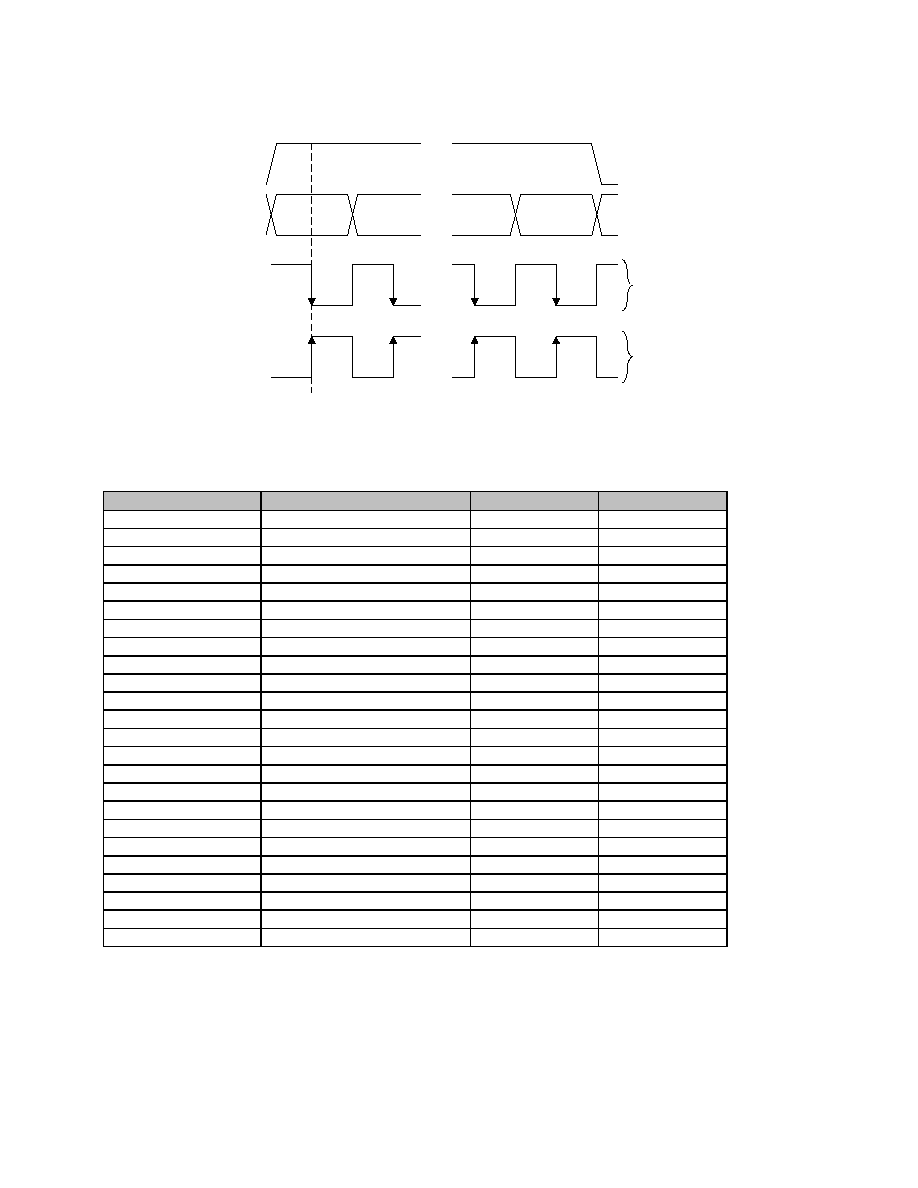
24-bit Input Mode (BSEL = 1)
P
0
IDCK+
D[23:0]
P
1
P
N-1
P
N
DE
IDCK+
First Edge Latch
DSEL = 0, EDGE = 0
DSEL = 0, EDGE = 1
Figure 9. Logical Interface Options for 24-bit Mode
24-bit Mode Data Mapping
Pin Name
P0
P1
P2
D23
R0[7]
R1[7]
R2[7]
D22
R0[6]
R1[6]
R2[6]
D21
R0[5]
R1[5]
R2[5]
D20
R0[4]
R1[4]
R2[4]
D19
R0[3]
R1[3]
R2[3]
D18
R0[2]
R1[2]
R2[2]
D17
R0[1]
R1[1]
R2[1]
D16
R0[0]
R1[0]
R2[0]
D15
G0[7]
G1[7]
G2[7]
D14
G0[6]
G1[6]
G2[6]
D13
G0[5]
G1[5]
G2[5]
D12
G0[4]
G1[4]
G2[4]
D11
G0[3]
G1[3]
G2[3]
D10
G0[2]
G1[2]
G2[2]
D9
G0[1]
G1[1]
G2[1]
D8
G0[0]
G1[0]
G2[0]
D7
B0[7]
B1[7]
B2[7]
D6
B0[6]
B1[6]
B2[6]
D5
B0[5]
B1[5]
B2[5]
D4
B0[4]
B1[4]
B2[4]
D3
B0[3]
B1[3]
B2[3]
D2
B0[2]
B1[2]
B2[2]
D1
B0[1]
B1[1]
B2[1]
D0
B0[0]
B1[0]
B2[0]
Notes:
1
In the figure, clock edges represented by arrows signify the latching edge.
2
In 24 bit mode, dual edge mode (DSEL = 1) is not supported.
3
Color Pixel Components: R = RED, G = GREEN, B = BLUE
4
Bit significance within a color: [7:0] = [MSB:LSB]
5
HSYNC and VSYNC are latched by the opposite edge of where data is latched.

Silicon Image, Inc.
Si
I
154
Si
I
/DS-0010-D
Revision 0.94
Subject to Change without Notice
9
Data De-skew
Input clock to data setup/hold time can be adjusted through the use of the de-skew feature. It should be noted
that it is the clock that is being adjusted. When DKEN is high, the configuration pins DK[3:1] or applicable I
2
C
registers can be used to vary the input setup/hold time by an amount T
CD
given by the formula
T
CD
= (DK[3:1] - 4)*T
STEP
.
Where:
T
CD
is the amount setup/hold timing variation
DK[3:1] is the setting of the de-skew configuration pins
T
STEP
is the step size
This feature can be used in both 12-bit or 24-bit mode.
If DKEN is set low, the DK[3:1] inputs are ignored, and the default setting of T
CD
= 0 is used.
CLK+
CLK-
000
111
D[23:0]
-T
CD
T
CD
default
10. Si
I
154 De-skewing feature timing
Silicon Image, Inc.
Si
I
154
Si
I
/DS-0010-D
Revision 0.94
Subject to Change without Notice
10
Pins Descriptions
Input Pin
Pin Name
Pin #
Type
Description
D23-D12
36-47
In
Top half of 24-bit pixel bus.
When BSEL = HIGH, this bus inputs the top half of the 24-bit pixel bus.
When BSEL = LOW, these bits are not used to input pixel data. In this
mode, the state of D[23:16] is input to the I
2
C register CFG. This allows 8-
bits of user configuration data to be read by the graphics controller through
the I2C interface (see I
2
C register definition). D[15:12] are reserved for SiI
use only and should be tied to GND when not in use.
D11≠D0
50-55,
58-63
In
Bottom half of 24-bit pixel bus / 12-bit pixel bus input.
When BSEL = HIGH, this bus inputs the bottom half of the 24-bit pixel bus.
When BSEL = LOW, this bus inputs Ω a pixel at every latch edge (both
falling and/or rising).
IDCK+
57
In
Input Data Clock +.
IDCK-
56
In
Input Data Clock ≠. This clock is only used in 12-bit mode when dual edge
clocking is turned off (DSEL = LOW). It is used to provide the ODD
latching edges for multi-phased clocking. If (BSEL = HIGH) or (DSEL =
HIGH) this pin is unused and should be tied to GND.
DE
2
In
Data enable. This signal is high when input pixel data is valid to the
transmitter and low otherwise. It is critical that this signal have the same
setup/hold timing as the data bus.
HSYNC
VSYNC
4
5
In
In
Horizontal Sync input control signal.
Vertical Sync input control signal.
Note: In 12 bit mode the HSYNC and VSYNC signals are latched by the
secondary clock edge.
CTL1/A1/DK1
CTL2/A2/DK2
CTL3/A3/DK3
8
7
6
In
The use of these multi-function inputs depends on the settings of ISEL and
DKEN. These inputs are regular high-swing CMOS level inputs. These
pins contain weak pull-down resistors so that if left unconnected, they will
be LOW.
ISEL = LOW, DKEN = LOW
General Purpose Input CTL[3:1] are active, for backward
compatibility. These pins must be used to send DC signals only.
ISEL = LOW, DKEN = HIGH
DK[3:1] are active, these inputs are used to select the de-skewing
setting for the input bus.
ISEL = HIGH, DKEN = HIGH
A[3:1] are active, these bits are used to set the lower 3 bits of the
I
2
C device address.
Status Pin
Pin Name
Pin #
Type
Description
MSEN
11
Out
Monitor Sense. This pin is an open collector output. The behavior of this
output depends on whether I
2
C interface is enabled or disabled.
I
2
C bus is disabled (ISEL = LOW)
A HIGH level indicates a powered on receiver is detected at the
differential outputs.
A LOW level indicates a powered on receiver is not detected.
This function can only be used in DC-coupling systems.
I
2
C bus is enabled (ISEL = HIGH)
The output is programmable through the I
2
C interface (see I
2
C
register definitions).
This function can only be used in DC-coupling systems.
An external 5K pull-up resistor is required on this pin.
Silicon Image, Inc.
Si
I
154
Si
I
/DS-0010-D
Revision 0.94
Subject to Change without Notice
11
Configuration/Programming Pins
Pin Name
Pin # Type
Description
ISEL/RST
13
In
I
2
C Interface Select. If HIGH, then the I
2
C interface is active. If LOW, the I
2
C is
inactive and the chip configuration is read from the configuration strapping pins.
This pin also acts as an asynchronous reset to the I
2
C interface controller. The
reset is active when this input is held LOW.
Note: When then the I
2
C interface is active, DKEN must be set high.
BSEL/SCL
15
In
Input bus select / I
2
C clock. This pin is an open collector input. If I
2
C bus is
enabled (ISEL = HIGH), then this pin is the I
2
C clock input. If the I
2
C is disabled
(ISEL = LOW), then this pin selects the input bus width.
Input Bus Select :
HIGH selects 24-bit input mode
LOW selects 12-bit input mode
DSEL/SDA
14
In
Dual edge clock select / I
2
C Data. This pin is an open collector input. If I
2
C bus is
enabled (ISEL = HIGH), then this pin is the I
2
C data line. If the I
2
C bus is disabled
(ISEL = LOW), then this pin selects whether dual edge clocking is used.
Dual edge clock select :
When HIGH, IDCK+ latches input data on both falling and rising clock
edges.
When LOW, IDCK+/IDCK- latches input data on only falling or rising
clock edges. See the differences between 12 and 24 bit mode below:
In 12-bit mode (BSEL = LOW):
If HIGH (dual edge), IDCK+ is used to latch data on both falling and
rising edges.
If LOW (single edge), IDCK+ latches 1
st
half data and IDCK- latches 2
nd
half data.
In 24-bit mode (BSEL = HIGH):
DSEL must be set LOW
EDGE/HTPLG
9
In
Edge select / Hot Plug input. If the I
2
C bus is enabled (ISEL = HIGH), then this pin
is used to monitor the "Hot Plug" detect signal (Please refer to the DVI
TM
or VESA
Æ
P&D
TM
and DFP standards). NOTE: This Input is ONLY 3.3V tolerant and has no
internal debouncer circuit.
If I
2
C bus is disabled (ISEL = LOW), then this pin selects the clock edge that will
latch the data. How the EDGE setting works depends on whether dual or single
edge latching is selected :
Dual Edge Mode (DSEL = HIGH)
EDGE = LOW,the primary edge (first/even latch edge after DE is
asserted) is the falling edge.
EDGE = HIGH,the primary edge (first/odd latch edge after DE is
asserted) is the rising edge.
Note:
In dual edge mode, the control signals HS and VS are only latched on
the secondary clock edge.
Single Edge Mode (DSEL = LOW)
EDGE = LOW, the falling edge of the clock is used to latch data.
EDGE = HIGH, the rising edge of the clock is used to latch data.
DKEN
35
In
De-Skewing enable.
This pin determines whether the de-skewing increments are to be read in through
the DK[3:1] pins or the General Purpose Input CTL[3:1] are active.
DKEN = LOW, ISEL = LOW
Default de-skewing setting is used and General Purpose Input
CTL[3:1] are active.
DKEN = HIGH, ISEL = LOW
DK[3:1] is used as the de-skewing setting. The de-skewing
increments are T
STEP
DKEN = HIGH, ISEL = HIGH
If I
2
C bus is enabled (ISEL = HIGH), then DKEN must be set high,
DK[3:1] are ignored and the de-skewing increments are selected through
the I
2
C interface (see the I
2
C register definitions).
Silicon Image, Inc.
Si
I
154
Si
I
/DS-0010-D
Revision 0.94
Subject to Change without Notice
12
Input Voltage Reference Pin
Pin Name
Pin # Type
Description
VREF
3
Analog
In
Input Reference Voltage. Selects the swing range of the digital parallel
data inputs (D[23:0], DE, VSYNC, and HSYNC).
When VREF is HIGH, the digital parallel data inputs are normal high swing
CMOS inputs.
When VREF is below 1.8V, the digital parallel data inputs are low swing
inputs. In low swing mode, VREF must be set to Ω of V
DDQ
.
Power Management Pin
Pin Name
Pin # Type
Description
PD
10
In
Power Down (active low). A High level indicates normal operation and a
Low level indicates power down mode. During power down mode,
digital input, output buffers and I2C interface are NOT disabled. The
PanelLink Digital core is powered down. Note that when ISEL = HIGH,
this pin should be tied LOW to ensure the chip is powered off when reset is
asserted.
Reserved
Pin Name
Pin # Type
Description
RESERVED
34
In
Must be tied LOW for normal operation.
Differential Signal Data Pins
Pin Name
Pin # Type
Description
TX0+
TX0-
TX1+
TX1-
TX2+
TX2-
25
24
28
27
31
30
Analog
Analog
Analog
Analog
Analog
Analog
TMDS
TM
Low Voltage Differential Signal output data pairs.
TXC+
TXC-
22
21
Analog
Analog
TMDS
TM
Low Voltage Differential Signal output clock pairs.
EXT_SWING
19
Analog Voltage Swing Adjust. A resistor should tie this pin to AVCC. This
resistance determines the amplitude of the voltage swing. For remote
display applications, 400
is recommended. For notebook computers,
680
is recommended.
Power and Ground Pin
Pin Name
Pin #
Type
Description
VCC
1,12,33
Power
Digital VCC, must be set to 3.3V nominal.
GND
16,48,64
Ground Digital GND.
AVCC
23,29
Power
Analog VCC, must be set to 3.3V nominal.
AGND
20,26,32
Ground Analog GND.
PVCC1
18
Power
PLL Analog VCC, must be set to 3.3V nominal.
PVCC2
49
Power
PLL Analog VCC, must be set to 3.3V nominal.
PGND
17
Ground PLL Analog GND.
Please refer to PanelLink Digital Basic Design/Application Guide (SiI-AN-0005)

Silicon Image, Inc.
Si
I
154
Si
I
/DS-0010-D
Revision 0.94
Subject to Change without Notice
13
I
2
C Register
I
2
Addr.
Bit 7
Bit 6
Bit 5
Bit 4
Bit 3
Bit 2
Bit 1
Bit 0
0x0
VND_IDL (RO)
0x1
VND_IDH (RO)
0x2
DEV_IDL (RO)
0x3
DEV_IDH (RO)
0x4
DEV_REV (RO)
0x5
RSVD[7:0] (RO)
0x6
FRQ_LOW (RO)
0x7
FRQ_HIGH (RO)
0x8
RSVD[1:0]
VEN (R/W)
HEN (R/W)
DSEL
(RW)
BSEL
(RW)
EDGE (RW)
PD (RW)
0x9
VLOW (RO)
MSEL[2:0] (RW)
TSEL
(RW)
RSEN
(RO)
HTPLG
(RO)
MDI (RW)
0xA
DK[3:1] (RW)
DKEN (RW)
CTL[3:1] (RW)
RSVD
(RW)
0xB
CFG[7:0] (D[23:16]) (RO)
0xC
VDJK [7:0] (RW) Please see Si
I
-AN-0022 for application specific values of this register.
8
0xD
RSVD[3:0] (RW)
RSVD[3:0] (RO)
0xE
RSVD[7:0] (RW)
0xF
RSVD[7:0] (RW)
Notes:
1
All values are Bit 7 [MSB] and Bit 0 [LSB].
2
RW = Read/Write register, RO = Read Only register.
3
RSVD = Reserved register. It is available for future use by Silicon Image, Inc.
4
Values in Bold/Italics are for Silicon Image, Inc. test and characterization.
5
Any read/write register that is RESERVED will require that the user always write the Si
I
recommended values.
6
There is no default value on reset. All registers must be written at least once before enabling.
7
All registers retain their values after a reset except PD and MSEL.
8
Please see Application Note "Si
I
154: Setting the VDJK I
2
C Register Value" (Si
I
-AN-0022) for application specific
values of this register.
Silicon Image, Inc.
Si
I
154
Si
I
/DS-0010-D
Revision 0.94
Subject to Change without Notice
14
I
2
C Register Definitions
Register Name
Access
Description
VND_IDL
RO
Vendor ID Low byte (0x01)
VND_IDH
RO
Vendor ID High byte (0x00)
DEV_IDL
RO
Device ID Low byte (0x04)
DEV_IDH
RO
Device ID High byte (0x00)
DEV_REV
RO
Device Revision (0x00)
FRQ_LOW
RO
Low frequency limit at 1-pixel/clock mode (MHz)
FRQ_HIGH
RO
High frequency limit at 1-pixel/clock mode MHz minus 65MHz (MHz)
PD
RW
Power Down mode(same function as PD pin)
0 ≠ Power Down
1 ≠ Normal operation
EDGE
RW
Edge Select (same function as EDGE pin)
0 ≠ Input data is falling edge latched (falling edge latched first in dual edge
mode)
1 ≠ Input data is rising edge latched (rising edge latched first in dual edge
mode)
BSEL
RW
Input Bus Select (same function as BSEL pin)
0 ≠ Input data bus is 12-bits wide
1 ≠ Input data bus is 24-bits wide
DSEL
RW
Dual Edge Clock Select (same function as DSEL pin)
0 ≠ Input data is single edge latched
1 ≠ Input data is dual edge latched
HEN
RW
Horizontal Sync Enable:
0 ≠ HSYNC input is transmitted as fixed LOW
1 ≠ HSYNC input is transmitted as is
VEN
RW
Vertical Sync Enable:
0 ≠ VSYNC input is transmitted as fixed LOW
1 ≠ VSYNC input is transmitted as is
MDI
RW
Monitor Detect Interrupt
0 ≠ Detection signal has changed logic level (write one to this bit to clear)
1 ≠ Detection signal has not changed state
HTPLG
RO
Hot Plug Detect input, the state of HTPLG pin can be read from this bit
RSEN
RO
This bit is HIGH if a powered on receiver is connected to the transmitter
outputs, LOW otherwise. This function is only available for use in DC-coupled
systems.
TSEL
RW
Interrupt Generation Method
0 ≠ Interrupt bit (MDI) is generated by monitoring RSEN
pt bit (MDI) is generated by monitoring HTPLG
MSEL[2:0]
RW
Select source of the MSEN output pin
000 ≠ Force MSEN outputs high (disabled)
001 ≠ Outputs the MDI bit (interrupt)
010 ≠ Output the RSEN bit (receiver detect)
011 ≠ Outputs the HTPLG bit (hot plug detect)
1xx ≠ RESERVED
VLOW
RO
This bit is a 1 if the VREF signal indicates low swing inputs. It is a 0 if VREF
indicates high swing inputs
CTL[3:1]
RW
General purpose inputs (same as CTL[3:1] pins)
CFG[7:0]
RO
Contains state of inputs D[23:16]. These pins can be used to provide user
selectable configuration data through the I
2
C bus. Only available in 12-bit
mode
VDJK[7:0]
RW
Please see Application Note "Si
I
154: Setting the VDJK I
2
C Register Value"
(Si
I
-AN-0022) for application specific values of this register.
Silicon Image, Inc.
Si
I
154
Si
I
/DS-0010-D
Revision 0.94
Subject to Change without Notice
15
I
2
C Register Definitions (cont'd)
Register Name
Access
Description
DK[3:1]
RW
De-Skewing Setting. Increment T
STEP
psec.
000 : 1 step -> minimum setup / maximum hold
001 : 2 step
010 : 3 step
011 : 4 step
100 : 5 step -> default
101 : 6 step
110 : 7 step
111 : 8 step -> maximum setup / minimum hold
DKEN
RW
De-Skewing Enable through DK[3:1] bits. High when enabled, Low otherwise.
I
2
C Slave Interface
The Si
I
154 slave state machine does not require an internal clock and supports only byte read and write (see
Figures below). Page mode is not supported. The 7-bit binary address of the I
2
C machine is "0111 A
3
A
2
A
1
X",
where A[3:1] are pin programmable or set to "000" by default.
S
A
2
A
1
A
0
A
C
K
S
A
2
A
1
A
0
A
C
K
A
C
K
P
Slave Address
Address
Slave Address
Data
Stop
Start
Start
Bus Activity :
SiI 154
Bus Activity :
Master
SDA Line
Figure 11. I
2
C Byte Read
S
A
2
A
1
A
0
A
C
K
A
C
K
P
Slave Address
Address
Data
Stop
Start
Bus Activity :
SiI 154
Bus Activity :
Master
SDA Line
A
C
K
Figure 12. I
2
C Byte Write

Silicon Image, Inc.
Si
I
154
Si
I
/DS-0010-D
Revision 0.94
Subject to Change without Notice
16
RESET Description
The input pin ISEL/RST serves as an asynchronous reset (active LOW) for the I
2
C slave controller in I
2
C mode.
The programming registers, that are accessible over the I
2
C bus, retain their previous values during and after
the reset except for PD and MSEL[2:0] register bits. All of the I
2
C registers must be manually set to ensure
proper operation. There are no default settings for the I
2
C registers. The minimum low time for proper reset is
T
CIP
. The state of these bits is set during the reset period according to the following rules:
∑
After a RESET, the Si
I
154 will be turned OFF. When reset is asserted, the Si
I
154 power down control bit,
PD, is forced LOW. When the SiI154 comes out of reset (ISEL/RST is set HIGH), the Si
I
154 will be turned
OFF. To turn the Si
I
154 back ON, the PD bit must be set HIGH over the I
2
C bus.
∑
After a RESET, MSEN output is disabled. When reset is asserted, MSEN[2:1] is forced to `000'. This
causes the MSEN output to be tri-stated.
Silicon Image, Inc.
Si
I
154
Si
I
/DS-0010-D
Revision 0.94
Subject to Change without Notice
17
Package Dimensions
64-pin TQPF Package Dimensions
64-pin Plastic TQFP
SiI164CT 64
LNNNNN.NLLL
XXYY
X.XX
Lead Length
1.00mm
Lead Width
0.22mm
Lead Pitch
0.50mm
Body Thickness
1.0 mm
Package Height
1.0mm max.
Clearance
0.15mm max.
Body Size 10.00mm
Footprint 12.00mm
Body Size 10.00mm
Footprint 12.00mm
Device #
Lot #
Date Code
SiI Rev. #
PanelLink
PanelLink
Æ
Figure 13. Si
I
154 Package Diagram
Silicon Image, Inc.
Si
I
154
Si
I
/DS-0010-D
Revision 0.94
Subject to Change without Notice
18
Copyright Notice
This manual is copyrighted by Silicon Image, Inc. Do not reproduce, transform to any other format, or send/transmit any part of this
documentation without the express written permission of Silicon Image, Inc.
Trademark Acknowledgment
Silicon Image, the Silicon Image logo,
PanelLink
Æ
, the
PanelLink
Æ
Digital logo
and TMDS
TM
are trademarks of Silicon Image, Inc.
VESA
Æ
is a registered trademark of Video Electronics Standards Association. TMDS
TM
is a licensed trademark of VESA
Æ
.
All other trademarks are the property of their respective holders.
Disclaimer
This document provides technical information for the user. Silicon Image, Inc. reserves the right to modify the information in this document
as necessary. The customer should make sure that it has the most recent data sheet version. Silicon Image, Inc. holds no responsibility
for any errors that may appear in this document. Customers should take appropriate action to ensure their use of the products does not
infringe upon any patents. Silicon Image, Inc. respects valid patent rights of third parties and does not infringe upon or assist others to
infringe upon such rights.
Part Ordering Number: Si
I
154CT64
© 1999 Silicon Image Inc. 11/99 Si
I/
DS-0010-D
Silicon Image, Inc.
Tel: (408) 873-3111, 1-888-PanelLink
10131 Bubb Road
Fax: (408) 873-0446
Cupertino, CA 95014
E-mail:
salessupport@siimage.com
USA
Web:
www.siimage.com
or
www.panellink.com