 | –≠–ª–µ–∫—Ç—Ä–æ–Ω–Ω—ã–π –∫–æ–º–ø–æ–Ω–µ–Ω—Ç: SII160 | –°–∫–∞—á–∞—Ç—å:  PDF PDF  ZIP ZIP |
Revision C
Subject to Change without Notice
Si
I
160
PanelLink
Æ
Digital Transmitter
April 2000
General Description
Features
The Si
I
160 transmitter uses PanelLink Digital technology to support
displays ranging from VGA to UXGA resolutions (25-165 MHz). The Si
I
160
transmitter supports up to true color panels (24 bit/pixel, 16.7M colors) in 1 or
2 pixels/clock mode, and also features an inter-pair skew tolerance up to 1 full
input clock cycle. An advanced on-chip jitter filter is also added to extend
tolerance to VGA clock jitter. Since all PanelLink products are designed on
scaleable CMOS architecture to support future performance requirements
while maintaining the same logical interface, system designers can be
assured that the interface will be fixed through a number of technology and
performance generations.
PanelLink Digital technology simplifies PC & display interface design by
resolving many of the system level issues associated with high-speed digital
design, providing the system designer with a digital interface solution that is
quicker to market and lower in cost.
∑
Scaleable Bandwidth: 25-165 MHz (VGA to UXGA)
∑
Low Power: 3.3V core operation
∑
High Skew Tolerance: 1 full input clock cycle (6ns at
165 MHz)
∑
Flexible panel interface: single or dual pixel in at up
to 24-bits
∑
Sync Detect: for Plug & Display "Hot Plugging"
∑
Cable Distance Support: over 5m with twisted-pair,
fiber-optics ready
∑
Compliant with DVI 1.0 (DVI is backwards
compatible with VESAÆ P&D
TM
and DFP)
Si
I
160
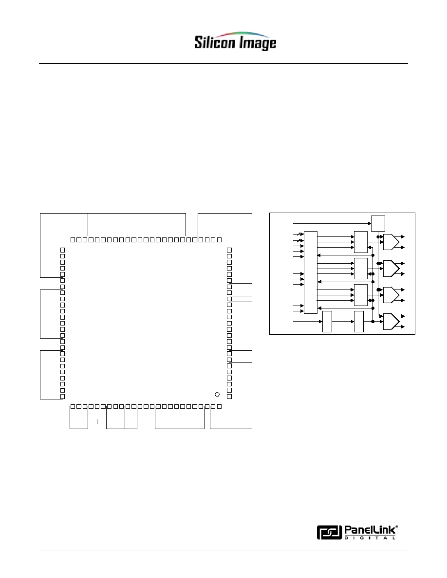
Pin Diagram
Functional Block Diagram
Data
Capture
Logic
DE
HSYNC
VSYNC
CTL1
CTL2
CTL3
EDGE
IDCK
EXT_SWING
Tx0
PIXS
DATA
DATA
24
DIE[23:0]
DIO[23:0]
Encoder
0
HSYNC
VSYNC
Encoder
1
Encoder
2
CTL1
DATA
CTL2
CTL3
24
Jitter
Filter
PLL
Swing
Control
Tx1
Tx2
TxC
Tx0+
Tx0-
Tx1+
Tx1-
Tx2+
Tx2-
TxC+
TxC-
DIE13
1
SiI 160
100-Pin TQFP
(Top View)
DIE12
2
DIE11
3
DIE10
4
DIE9
5
DIE8
6
GND
7
VCC
8
DIE7
9
DIE6
10
DIE5
11
DIE4
12
DIE3
13
DIE2
14
DIE1
15
DIE0
16
IVCC
17
PVCC1
18
PGND1
19
RESERVED
20
RESERVED
21
RESERVED
22
RESERVED
23
EDGE
24
PIXS
25
PD
26
RESERVED
27
RESERVED
28
RESERVED
29
VCC
30
GND
31
EXT_SWING
32
AGND
33
TXC-
34
TXC+
35
AVCC
36
AGND
37
AVCC
38
TX0-
39
TX0+
40
AGND
41
TX1-
42
TX1+
43
AVCC
44
TX2-
45
TX2+
46
AGND
47
DIO23
48
DIO22
49
DIO21
50
75
DIO1
74
DIO2
73
DIO3
72
DIO4
71
DIO5
70
DIO6
69
DIO7
68
GND
67
IVCC
66
DIO8
65
DIO9
64
DIO10
63
DIO11
62
DIO12
61
DIO13
60
DIO14
59
DIO15
58
GND
57
VCC
56
DIO16
55
DIO17
54
DIO18
53
DIO19
52
DIO20
51
DIO0
D
I
E
1
4
100
DIE15
99
IVCC
98
DIE16
97
DIE17
96
DIE18
95
DIE19
94
DIE20
9
3
DIE21
9
2
DIE22
91
DIE23
90
GND
89
VCC
88
RESERVED
87
PGND2
86
PVCC2
8
5
CTL1
8
4
CTL2
83
CTL3
8
2
IVCC
81
IDCK
80
GND
79
DE
78
VSYNC
7
7
HSYNC
7
6
DIFFERENTIAL
SIGNAL
ODD 8-bits RED
EVEN 8-bits RED
ODD 8-bits GREEN
EVEN 8-bits GREEN
ODD 8-bits BLUE
EVEN 8-bits BLUE
CONFIG. PINS
PLL
PLL
CONTROLS
INPUT CLOCK
GPI

Silicon Image, Inc.
SiI 160
SiI-DS-0008-C
Revision C
Subject to Change without Notice
2
Absolute Maximum Conditions
Note: Permanent device damage may occur if absolute maximum conditions are exceeded.
Functional operation should be restricted to the conditions described under Normal Operating Conditions.
Symbol
Parameter
Min
Typ
Max
Units
V
CC
Supply Voltage 3.3V
-0.3
4.0
V
V
I
Input Voltage
-0.3
V
CC
+ 0.3
V
V
O
Output Voltage
-0.3
V
CC
+ 0.3
V
T
A
Ambient Temperature (with power applied)
-25
105
∞
C
T
STG
Storage Temperature
-40
125
∞
C
P
PD
Package Power Dissipation
1
W
Normal Operating Conditions
Symbol
Parameter
Min
Typ
Max
Units
V
CC
Supply Voltage
3.00
3.3
3.6
V
V
CCN
Supply Voltage Noise
100
mV
P-P
T
A
Ambient Temperature (with power applied)
0
25
70
∞
C
DC Digital I/O Specifications
Under normal operating conditions unless otherwise specified.
Symbol
Parameter
Conditions
Min
Typ
Max
Units
V
IH
High-level Input Voltage
2
V
V
IL
Low-level Input Voltage
0.8
V
V
OH
High-level Output Voltage
2.4
V
V
OL
Low-level Output Voltage
0.4
V
V
CINL
Input Clamp Voltage
1
I
CL
= -18mA
GND -0.8
V
V
CIPL
Input Clamp Voltage
1
I
CL
= 18mA
IVCC + 0.8
V
V
CONL
Output Clamp Voltage
1
I
CL
= -18mA
GND -0.8
V
V
COPL
Output Clamp Voltage
1
I
CL
= 18mA
OVCC + 0.8
V
I
IL
Input Leakage Current
-10
10
µ
A
Note:
1
Guaranteed by design.
DC Specifications
Under normal operating conditions unless otherwise specified.
Symbol
Parameter
Conditions
Min
Typ
Max
Units
V
OD
Differential Voltage
Single ended peak to peak amplitude
R
LOAD
= 50
R
EXT_SWING
= 510
510
550
590
mV
V
DOH
Differential High-level Output Voltage
1
AVCC
V
I
DOS
Differential Output Short Circuit Current
1
V
OUT
= 0 V
5
µ
A
I
PD
Power-down Current
2
TBD
mA
I
CCT
Transmitter Supply Current
DCLK= 165 MHz, 1-pixel/clock mode,
(DCLK= 112 MHz, 1-pixel/clock mode)
R
EXT_SWING
= 680
,
IVCC = VCC,
Typical Pattern
3
70
95
mA
DCLK= 165 MHz, 1-pixel/clock mode,
(DCLK= 112 MHz, 1-pixel/clock mode)
R
EXT_SWING
= 680
,
IVCC = VCC,
Worse Case Pattern
4
90
110
mA
Note:
1
Guaranteed by design.
2
Assumes all inputs to the transmitter are not toggling.
3
The Typical Pattern contains a gray scale area, checkerboard area, and text.
4
Black and white checkerboard pattern, each checker is one pixel wide.
Silicon Image, Inc.
SiI 160
SiI-DS-0008-C
Revision C
Subject to Change without Notice
3
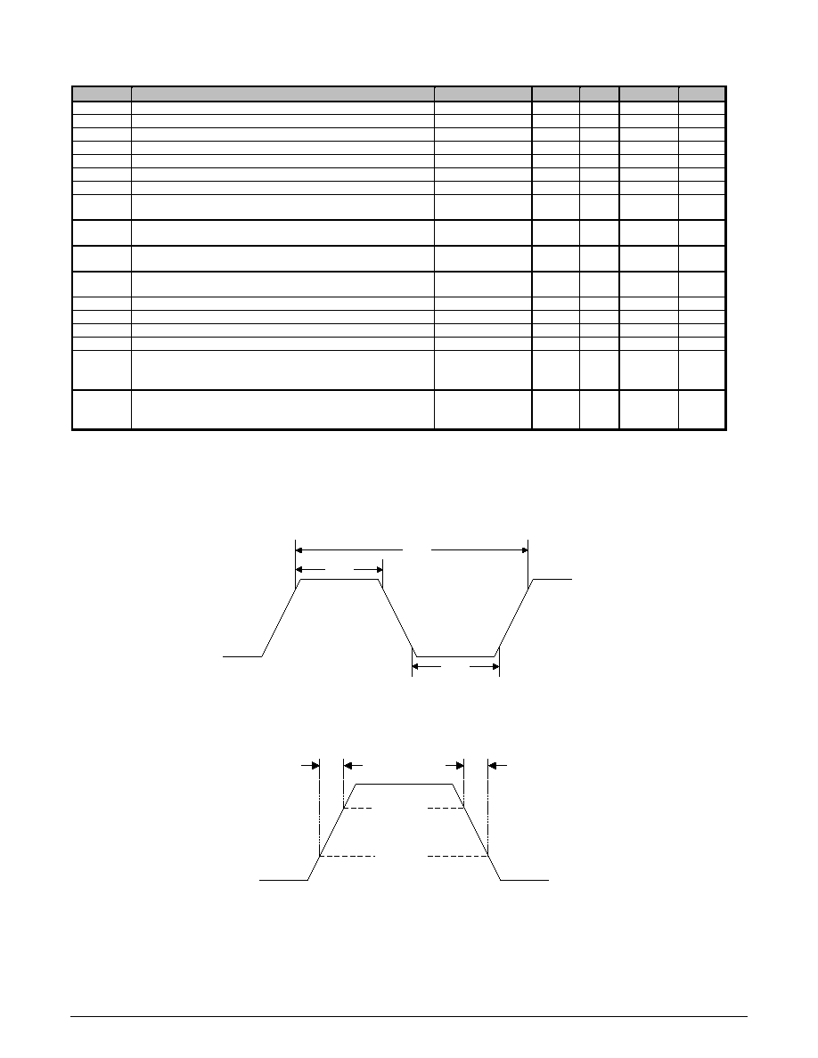
AC Specifications
Under normal operating conditions unless otherwise specified.
Symbol
Parameter
Conditions
Min
Typ
Max
Units
T
CIP
IDCK Period, 1 Pixel/Clock
6.06
40
ns
F
CIP
IDCK Frequency, 1 Pixel/Clock
25
165
MHz
T
CIP
IDCK Period, 2 Pixels/Clock
12.3
80
ns
F
CIP
IDCK Frequency, 2 Pixels/Clock
12.5
81
MHz
T
CIH
IDCK High Time at 165MHz
2
ns
T
CIL
IDCK Low Time at 165MHz
2
ns
T
IJIT
Worst Case IDCK Clock Jitter
2,3
2
ns
T
SIDF
Data, DE, VSYNC, HSYNC, and CTL[3:1]
Setup Time to IDCK falling edge
EDGE = 0
1.5
ns
T
HIDF
Data, DE, VSYNC, HSYNC, and CTL[3:1]
Hold Time from IDCK falling edge
EDGE = 0
1.5
ns
T
SIDR
Data, DE, VSYNC, HSYNC, and CTL[3:1]
Setup Time to IDCK rising edge
1
EDGE = 1
1.5
ns
T
HIDR
Data, DE, VSYNC, HSYNC, and CTL[3:1]
Hold Time from IDCK rising edge
1
EDGE = 1
1.5
ns
T
DDF
VSYNC, HSYNC, and CTL[3:1] Delay from DE falling edge
1
T
CIP
ns
T
DDR
VSYNC, HSYNC, and CTL[3:1] Delay to DE rising edge
1
T
CIP
ns
T
HDE
DE high time
1
8000T
CIP
ns
T
LDE
DE low time
1
10T
CIP
ns
S
LHT
Small Swing Low-to-High
Transition Time
R
LOAD
= 50
R
EXT_SWING
=
510
170
200
230
ns
S
HLT
Small Swing High-to-Low
Transition Time
R
LOAD
= 50
R
EXT_SWING
=
510
170
200
230
ns
Notes:
1
Guaranteed by design.
2
Jitter can be estimated by 1) triggering a digital scope at the rising of input clock and 2) measuring the peak to peak time spread
of the rising edge of the input clock 1
µ
s after the trigger.
3
Actual jitter tolerance may be higher depending on the frequency of the jitter.
Timing Diagrams
Figure 1. Clock Cycle/High/Low Times
Figure 2. Small Swing Transition Times
T
CIH
T
CIL
T
CIP
V
IH
V
IH
V
IL
V
IL
S
LHT
20% V
OD
80% V
OD
S
HLT
Silicon Image, Inc.
SiI 160
SiI-DS-0008-C
Revision C
Subject to Change without Notice
4
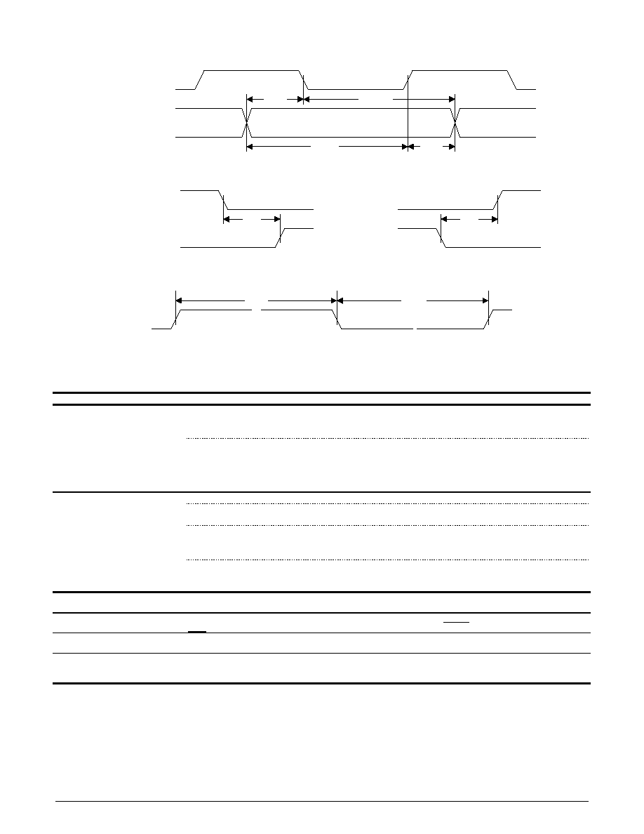
Input Timing
DIE[23:0]/
DIO[23:0], DE,
HSYNC,VSYNC,
CTL[3:1]
IDCK
T
SIDF
T
HIDF
T
SIDR
T
HIDR
Figure 3. Input Data Setup/Hold Times to IDCK
T
DDR
T
DDF
DE
VSYNC, HSYNC,
CTL[3:1]
DE
VSYNC, HSYNC,
CTL[3:1]
Figure 4. VSYNC, HSYNC, and CTL[3:1] Delay Times from DE
DE
T
HDE
T
LDE
Figure 5. DE High/Low Times
Input Pin Description
Pin Name
Pin #
Type
Description
DIE23-
DIE0
See Si
I
160 Pin
Diagram
In
Even Input Data[23:0] corresponds to 24-bit pixel data for 1-pixel/clock input mode or to the first 24-bit
pixel data for 2-pixels/clock mode.
Input data is synchronized to input data clock (IDCK).
Data can be latched on the rising or the falling edge of IDCK depending on whether EDGE is high or low,
respectively.
Refer to the TFT and DSTN Signal Mapping application notes (Si
I
/AN-0008-A and Si
I
/AN-0007-A,
respectively) which tabulate the relationship between the input data to the transmitter and output data from
the receiver.
DIO23 ≠
DIO0
See
SiI
160 Pin
Diagram
In
Input Odd Data[23:0] corresponds to the second 24-bit pixel data for 2-pixels/clock mode.
In 1-pixel/clock mode, these inputs are a don't care. Recommendation is to tie them low for lower power
consumption.
Input data is synchronized to input data clock (IDCK).
Data can be latched on the rising or the falling edge of IDCK depending on whether EDGE is high or low,
respectively.
Refer to the TFT and DSTN Signal Mapping application notes (Si
I
/
AN-0008-A and Si
I
/
AN-0007-A,
respectively) which tabulate the relationship between the input data to the transmitter and output data from
the receiver.
IDCK
80
In
Input Data Clock. Input data and control signals can be valid either on the falling or the rising edge of
IDCK as selected by the EDGE pin.
DE
78
In
Input Data Enable. This signal qualifies the active data area. DE is always required by the transmitter and
must be high during active display time and low during blanking time.
HSYNC
VSYNC
76
77
In
In
Horizontal Sync input control signal.
Vertical Sync input control signal.
CTL1
CTL2
CTL3
84
83
82
In
In
In
General input control signal 1.
General input control signal 2.
General input control signal 3.
Silicon Image, Inc.
SiI 160
SiI-DS-0008-C
Revision C
Subject to Change without Notice
5
Configuration Pin Description
Pin Name
Pin #
Type
Description
EDGE
24
In
Data/Control Latching Edge. A low level indicates that all input signals (DIE/DIO[23:0], HSYNC, VSYNC, DE,
and CTL[3:1]) are latched on the falling edge of IDCK, while a high level (3.3V) indicates that all input signals
are latched on the rising edge of IDCK.
PIXS
25
In
Pixel Select. A low level indicates one pixel (up to 24-bits) per clock mode using DIE[23:0]. A high level
(3.3V) indicates two pixels (up to 48-bits) per clock mode using DIE[23:0] for the first pixel and DIO[23:0] for
the second pixel.
RESERVED
27
In
This input must be tied high (3.3V), but we recommend that this pin have an option to tie it low.
Power Management Pin Description
Pin Name
Pin #
Type
Description
PD
26
In
Power Down (active low). A high level (3.3V) indicates normal operation and a low level (GND) indicates
power down mode. During power down mode, all data (DIE/DIO[23:0]), data enable (DE), clock (IDCK) and
control signals (HSYNC, VSYNC, CTL[3:1]), input buffers are disabled, all output buffers are tri-stated, and all
internal circuitry is powered down.
Differential Signal Data Pin Description
Pin Name
Pin #
Type
Description
TX0+
TX0-
TX1+
TX1-
TX2+
TX2-
40
39
43
42
46
45
Analog
Analog
Analog
Analog
Analog
Analog
TMDS Low Voltage Differential Signal output data pairs.
TXC+
TXC-
35
34
Analog
Analog
TMDS Low Voltage Differential Signal output data pairs.
EXT_SWING
32
Analog
Voltage Swing Adjust. A resistor should tie this pin to AVCC. The amplitude of the voltage swing is
determined by this resistance. For remote display applications, 400
is recommended. For notebook
computers, 680
is recommended.
Reserved Pin Description
Pin Name
Pin #
Type
Description
RESERVED
RESERVED
RESERVED
RESERVED
RESERVED
RESERVED
RESERVED
20
21
22
23
28
29
87
In
In
In
In
In
In
In
Reserved for future use. Must be tied HIGH for normal operation.
Reserved for future use. Must be tied LOW for normal operation.
Reserved for future use. Must be tied HIGH for normal operation.
Reserved for future use. Must be tied HIGH for normal operation.
Reserved for future use. Must be tied HIGH for normal operation.
Reserved for future use. Must be tied HIGH for normal operation.
Reserved for future use. Must be tied HIGH for normal operation.
Power and Ground Pin Description
Pin Name
Pin #
Type
Description
VCC
8,30,56,88
Power
Digital Core VCC, must be set to 3.3V.
GND
7,31,57,67,79,89
Ground
Digital GND.
IVCC
17,66,81,98
Power
Input VCC, must be set to 3.3V.
AVCC
36,38,44
Power
Analog VCC, must be set to 3.3V.
AGND
33,37,41,47
Ground
Analog GND.
PVCC1
18
Power
PLL Analog VCC, must be set to 3.3V.
PVCC2
85
Power
PLL Analog VCC, must be set to 3.3V.
PGND1
19
Ground
PLL Analog GND. PGND1 should not be directly connected to PGND2 before being
connected to the GROUND plane. They should be connected individually to the GROUND
plane.
PGND2
86
Ground
PLL Analog GND. PGND1 should not be directly connected to PGND2 before being
connected to the GROUND plane. They should be connected individually to the GROUND
plane.
Application Information
To obtain the most updated Application Notes and other useful information for your design application, please visit the Silicon Image
web site at www.siimage.com, or contact your local Silicon Image sales office.
Silicon Image, Inc.
SiI 160
SiI-DS-0008-C
Revision C
Subject to Change without Notice
6
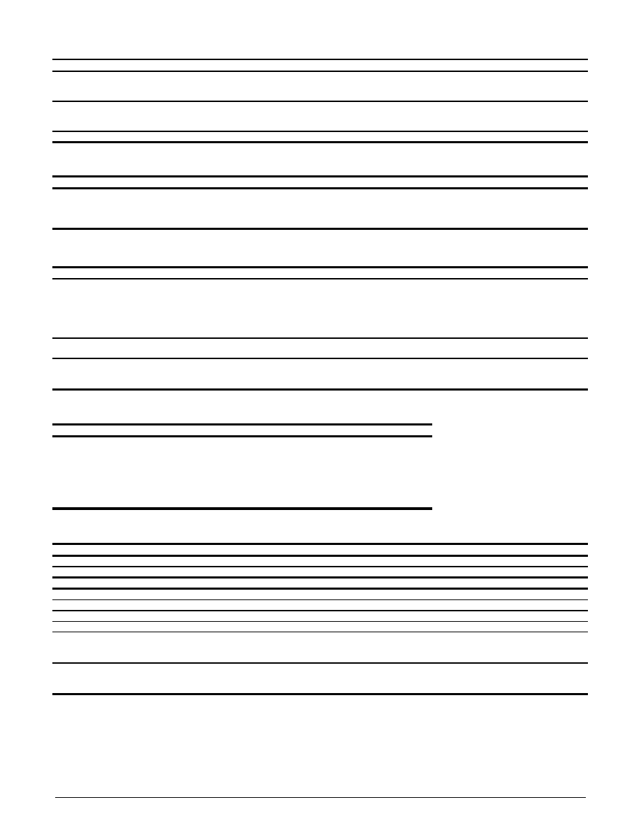
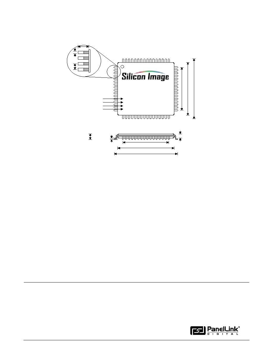
Package Dimensions
100-pin TQFP Package Dimensions
Ordering Information:
Part Number: SiI160CT100
Copyright Notice
This manual is copyrighted by Silicon Image, Inc. Do not reproduce, transform to any other format, or send/transmit any part of this
documentation without the express written permission of Silicon Image, Inc.
Trademark Acknowledgment
Silicon Image, the Silicon Image logo, PanelLink and the PanelLink Digital logo are trademarks or registered trademarks of Silicon Image,
Inc. All other trademarks are the property of their respective holders.
Disclaimer
This document provides technical information for the user. Silicon Image, Inc. reserves the right to modify the information in this document
as necessary. The customer should make sure that they have the most recent data sheet version. Silicon Image, Inc. holds no responsibility
for any errors that may appear in this document. Customers should take appropriate action to ensure their use of the products does not
infringe upon any patents. Silicon Image, Inc. respects valid patent rights of third parties and does not infringe upon or assist others to
infringe upon such rights.
© 2000 Silicon Image, Inc. 4/00 Si
I
-DS-0008-C
Silicon Image, Inc.
Tel:
408-616-4000
1060 E. Arques Avenue
Fax:
408-830-9530
Sunnyvale, CA 94086
E-Mail: salessupport@siimage.com
USA
Web:
www.siimage.com
www.panellink.com
100-pin Plastic TQFP
SiI160 CT100
LNNNNN.NLLL
XXYY
X.XX
Lead Length
1.00mm
Lead Width
0.20mm
Lead Pitch
0.50mm
Body Thickness
1.05 mm max.
Package Height
1.20mm max.
Clearance
0.15mm max.
Body Size 14.00mm
Footprint 16.00mm
Body Size 14.00mm
Footprint 16.00mm
Device #
Lot #
Date Code #
SiI Rev. #
12.00mm
12.00mm
PanelLink
PanelLink
PanelLink
PanelLink
Æ