CAN 2.0B
Copyright © 2004 by Silicon Laboratories
10.11.2004
UART1
SMBus
SPI Bus
PCA
Timers
0,1,2,3,4
VDD
VDD
VDD
DGND
DGND
DGND
RST
XTAL1
XTAL2
Internal
2%
Oscillator
P2.0/CPx
P2.7/CPx
P0.0
P0.7
VREF
AIN0.0
AIN0.1
AIN0.2
AIN0.3
VREF
UART0
MONEN
WDT
VREFA
P7 Latch
P5 Latch
P6 Latch
P5
DRV
P6
DRV
P4
DRV
Addr [15:8]
Addr [7:0]
Ctrl Latch
Data Latch
A
M
U
X
8:2
TEMP
SENSOR
P0
Drv
P1
Drv
P2
Drv
P3
Drv
Port
0,1,2,3
&4
Latches
CAN
2.0B
CANRX
CANTX
8
0
5
1
C
o
r
e
Reset
A
M
U
X
ADC
100 ksps
(10-Bit)
External Data Memory Bus
32x136
CANRAM
256 byte
RAM
4 kB
XRAM
P3.0/AINAMUX0
P3.7/AINAMUX7
P1.0
P1.7
64 kB
FLASH
System
Clock
External
Oscillator
Circuit
VDD
Monitor
C
R
O
S
S
B
A
R
Data [7:0]
Address [15:0]
Bus Control
Digital Power
Port 4 <from crossbar>
P2.1
P2.0
+
-
CP0
P2.3
P2.2
+
-
CP1
P2.5
P2.4
+
-
CP2
SFR Bus
P7
DRV
Debug HW
Boundary Scan
JTAG
Logic
TCK
TMS
TDI
TDO
AGND
AGND
AV+
AV+
Analog Power
Prog
Gain
HVAIN+
HVAIN-
HVREF
HVCAP
HVAMP
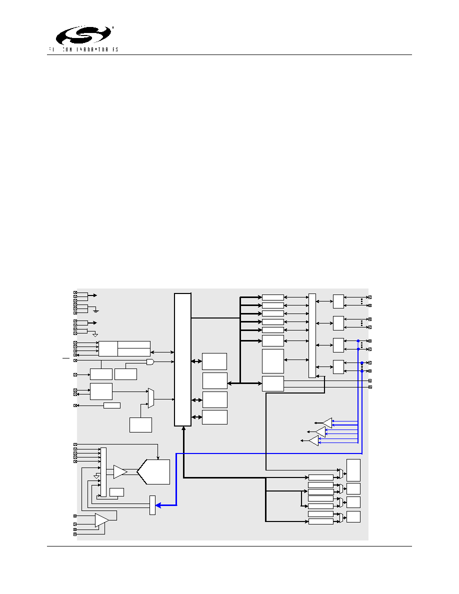
C8051F045
25 MIPS, 64 kB Flash, 10-Bit ADC, 64-Pin Mixed-Signal MCU
Analog Peripherals
10-Bit ADC
-
±1 LSB INL; guaranteed monotonic
-
Programmable throughput up to 100 ksps
-
13 external inputs; programmable as single-ended or differential
-
Programmable amplifier gain: 16, 8, 4, 2, 1, 0.5
-
Data-dependent windowed interrupt generator
-
Built-in temperature sensor (±3 ∞C)
High-Voltage Differential Amplifier
-
60 V common mode input range
-
Offset adjust from ≠60 to +60 V
-
16 gain settings from 0.05 to 16
Three Comparators
Internal Voltage Reference
Precision V
DD
Monitor/Brown-out Detector
On-Chip JTAG Debug & Boundary Scan
-
On-chip debug circuitry facilitates full speed, non-intrusive in-system
debug (no emulator required)
-
Provides breakpoints, single stepping, watchpoints, stack monitor, pro-
gram trace memory
-
Inspect/modify memory and registers
-
Superior performance to emulation systems using ICE-chips, target
pods, and sockets
-
IEEE1149.1 compliant boundary scan
High-Speed 8051 µC Core
-
Pipelined instruction architecture; executes 70% of instructions in 1 or 2
system clocks
-
Up to 25 MIPS throughput with 25 MHz system clock
-
Expanded interrupt handler
Memory
-
4352 bytes data RAM
-
64 kB Flash; in-system programmable in 512-byte sectors (512 bytes
are reserved)
-
External parallel data memory interface
CAN Bus 2.0B
-
32 message objects
-
"Mailbox" implementation only interrupts CPU when needed
Digital Peripherals
-
32 port I/O; all are 5 V tolerant
-
Hardware SMBusTM (I2CTM compatible), SPITM, and two UART serial
ports available concurrently
-
Programmable 16-bit counter array with 6 capture/compare modules
-
5 general-purpose 16-bit counter/timers
-
Dedicated watchdog timer; bidirectional reset
-
Real-time clock mode using timer 3 or PCA
Clock Sources
-
Internal programmable 2% oscillator: up to 25 MHz
-
External oscillator: Crystal, RC, C, or Clock
Supply Voltage: 2.7 to 3.6 V
-
Typical operating current: 10 mA at 25 MHz
-
Multiple power saving sleep and shutdown mode
64-Pin TQFP
Temperature Range: ≠40 to +85 ∞C
CAN 2.0B
Copyright © 2004 by Silicon Laboratories
10.11.2004
Silicon Laboratories and Silicon Labs are trademarks of Silicon Laboratories Inc.
Other products or brandnames mentioned herein are trademarks or registered trademarks of their respective holders
C8051F045
25 MIPS, 64 kB Flash, 10-Bit ADC, 64-Pin Mixed-Signal MCU
Selected Electrical Specifications
(T
A
= ≠40 to +85 C∞, V
DD
= 2.7 V unless otherwise specified)
Parameter
Conditions
Min
Typ
Max
Units
Global Characteristics
Supply Voltage
2.7
--
3.6
V
Supply Current with
CPU active
Clock = 25 MHz
Clock = 1 MHz
Clock = 32 kHz; V
DD
Monitor Enabled
--
10
0.5
20
--
mA
mA
µA
Supply Current (shutdown)
Oscillator off; V
DD
Monitor Disabled
--
0.1
--
µA
Clock Frequency Range
DC
--
25
MHz
A/D Converter
Resolution
--
10
--
bits
Integral Nonlinearity
--
--
±1
LSB
Differential Nonlinearity
Guaranteed Monotonic
±1
LSB
Signal-to-Noise Plus
Distortion
59
--
--
dB
Throughput Rate
--
--
100
ksps
Input Voltage Range
0
--
VREF
V
Comparators
Supply Current
(each Comparator)
--
1.5
--
µA
Response Time
(CP+ ≠ CP-) = 100 mV
--
4
--
µs
Package Information
A
A1
A2
b
D
D1
e
E
E1
-
0.05
0.95
0.17
-
-
-
-
-
-
-
-
0.22
12.00
10.00
0.50
12.00
10.00
1.20
0.15
1.05
0.27
-
-
-
-
-
MIN
(mm)
NOM
(mm)
MAX
(mm)
1
64
E
E1
e
A1
b
D
D1
PIN 1
DESIGNATOR
A2
A
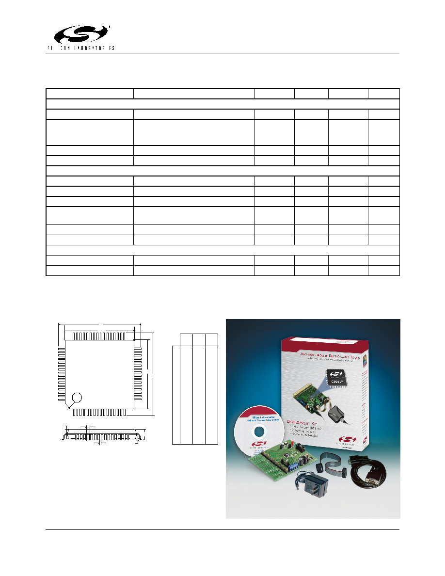
C8051F040DK Development Kit