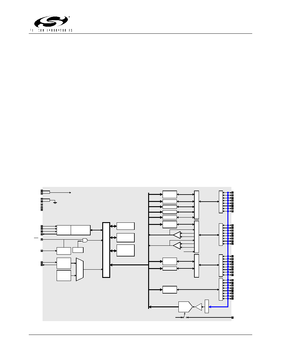
General Purpose
Copyright © 2005 by Silicon Laboratories
5.5.2005
Port 0
Latch
Port 1
Latch
JTAG
Logic
UART
8 kB
FLASH
256 byte
RAM
VDD
Monitor
SFR Bus
Port 2
Latch
Port 3
Latch
8
0
5
1
C
o
r
e
Timer 0
Timer 1
Timer 2
12-bit
100 ksps
ADC
A
M
U
X
CP0
CP1
AIN0-AIN31
P1.0/CP0+
P1.1/CP0-
P1.2/CP0
P1.3/CP1+
P1.4/CP1-
P1.5/CP1
P1.6/SYSCLK
P1.7
P
1
D
r
v
P0.0/TX
P0.1/RX
P0.2//INT0
P0.3//INT1
P0.4/T0
P0.5/T1
P0.6/T2
P0.7/T2EX
P
0
D
r
v
P3.0
P3.1
P3.2
P3.3
P3.4
P3.5
P3.6
P3.7
P
3
D
r
v
P2.0/NSS
P2.1/MISO
P2.2/MOSI
P2.3/SCK
P2.4
P2.5
P2.6
P2.7
P
2
D
r
v
CP0+
CP0-
CP1+
CP1-
P
0
M
U
X
Reset
External
Oscillator
Circuit
System Clock
Internal
Oscillator
Analog/Digital
Power
Debug HW
P
1
M
U
X
CP0
CP1
VDD
P
2
M
U
X
SPI
VREF
1024 byte
XRAM
WDT
PGA
SYSCLK
TCK
TMS
TDI
TDO
VDD
VDD
GND
GND
RST
XTAL1
XTAL2
NC
NC
NC
MONEN
C8051F206
25 MIPS, 8 kB Flash, 12-Bit ADC, 48-Pin Mixed-Signal MCU
Analog Peripherals
12-Bit ADC
-
No missing codes
-
Programmable throughput up to 100 ksps
-
32 external inputs (each port I/O can be configured as an ADC input on-
the-fly)
-
Programmable amplifier gain: 16, 8, 4, 2, 1, 0.5
-
Data-dependent windowed interrupt generator
-
V
REF
from external pin or V
DD
Two comparators
-
Programmable hysteresis
-
Configurable to generate interrupts or reset
V
DD
Monitor and Brown-out Detector
On-Chip JTAG Debug
-
On-chip emulation circuitry facilitates full-speed, non-intrusive, in-circuit
emulation
-
Supports breakpoints, single stepping, watchpoints, inspect/modify
memory, and registers
-
Superior performance to emulation systems using ICE-chips, target
pods, and sockets
-
Fully compliant with IEEE 1149.1 specification
Supply Voltage: 2.7 to 3.6 V
-
Typical operating current: 9 mA at 25 MHz
-
Typical stop mode current: <0.1 µA
Temperature Range: ≠40 to +85 ∞C
High-Speed 8051 µC Core
-
Pipelined instruction architecture; executes 70% of instructions in 1 or 2
system clocks
-
Up to 25 MIPS throughput with 25 MHz system clock
-
Expanded interrupt handler; up to 21 interrupt sources
Memory
-
1280 bytes data RAM
-
8 kB Flash; in-system programmable in 512 byte sectors (512 bytes are
reserved)
Digital Peripherals
-
32 port I/O; all are 5 V tolerant
-
Hardware SPITM and UART serial ports available concurrently
-
3 general-purpose 16-bit counter/timers
-
Dedicated watchdog timer; bidirectional reset
Clock Sources
-
Internal programmable oscillator: 2≠16 MHz
-
External oscillator: Crystal, RC, C, or Clock
-
Can switch between clock sources on-the-fly
Package
-
48-pin TQFP (standard lead and lead-free packages)
Ordering Part Numbers
-
Lead-free package: C8051F206-GQ
-
Standard package: C8051F206
General Purpose
Copyright © 2005 by Silicon Laboratories
5.5.2005
Silicon Laboratories and Silicon Labs are trademarks of Silicon Laboratories Inc.
Other products or brandnames mentioned herein are trademarks or registered trademarks of their respective holders
C8051F206
25 MIPS, 8 kB Flash, 12-Bit ADC, 48-Pin Mixed-Signal MCU
Selected Electrical Specifications
(T
A
= ≠40 to +85 C∞, V
DD
= 2.7 V unless otherwise specified)
PARAMETER CONDITIONS
MIN
TYP
MAX
UNITS
GLOBAL CHARACTERISTICS
Digital Supply Voltage
2.7
3.6
V
Digital Supply Current
with CPU active
Clock = 25 MHz
Clock = 1 MHz
Clock = 32 kHz; V
DD
Monitor Enabled
9
0.4
20
mA
mA
µA
Digital Supply Current
(shutdown)
Oscillator not running; V
DD
Monitor
Enabled
Oscillator not running; V
DD
Monitor
Disabled
10
0.1
µA
µA
Digital Supply RAM Data
Retention Voltage
1.5 V
CPU & DIGITAL I/O PORTS
Clock Frequency Range
DC
25
MHz
Port Output High Voltage
I
OH
= ≠3 mA, Port I/O push-pull
V
DD
≠ 0.7
V
Port Output Low Voltage
I
OL
= 8.5 mA
0.6
V
Input High Voltage
0.7 x V
DD
V
Input Low Voltage
0.3 x V
DD
V
SPI Bus Clock Frequency fCLK=MCU Clock; SPI Master Mode
fCLK/2
MHz
A/D CONVERTER
Resolution
12
bits
Integral Nonlinearity
±1
±2
LSB
Differential Nonlinearity
Guaranteed Monotonic
±1
LSB
Signal-to-Noise Plus
Distortion
64
dB
Throughput Rate
100
ksps
Input Voltage Range
0
V
REF
V
COMPARATORS
Supply
Current (each
Comparator)
1.3 µA
Response Time
| CP+ ≠ CP- | = 100 mV
4
µs
Input Voltage Range
≠0.25
VDD + 0.25
V
Input Bias Current
≠5
0.001
+5
nA
Input Offset Voltage
≠10
+10
mV
Package Information
A
A1
A2
b
D
D1
e
E
E1
-
0.05
0.95
0.17
-
-
-
-
-
-
-
1.00
0.22
9.00
7.00
0.50
9.00
7.00
1.20
0.15
1.05
0.27
-
-
-
-
-
MIN
(mm)
NOM
(mm)
MAX
(mm)
E
E1
D
D1
48
1
A1
e
b
PIN 1
IDENTIFIER
A2
A
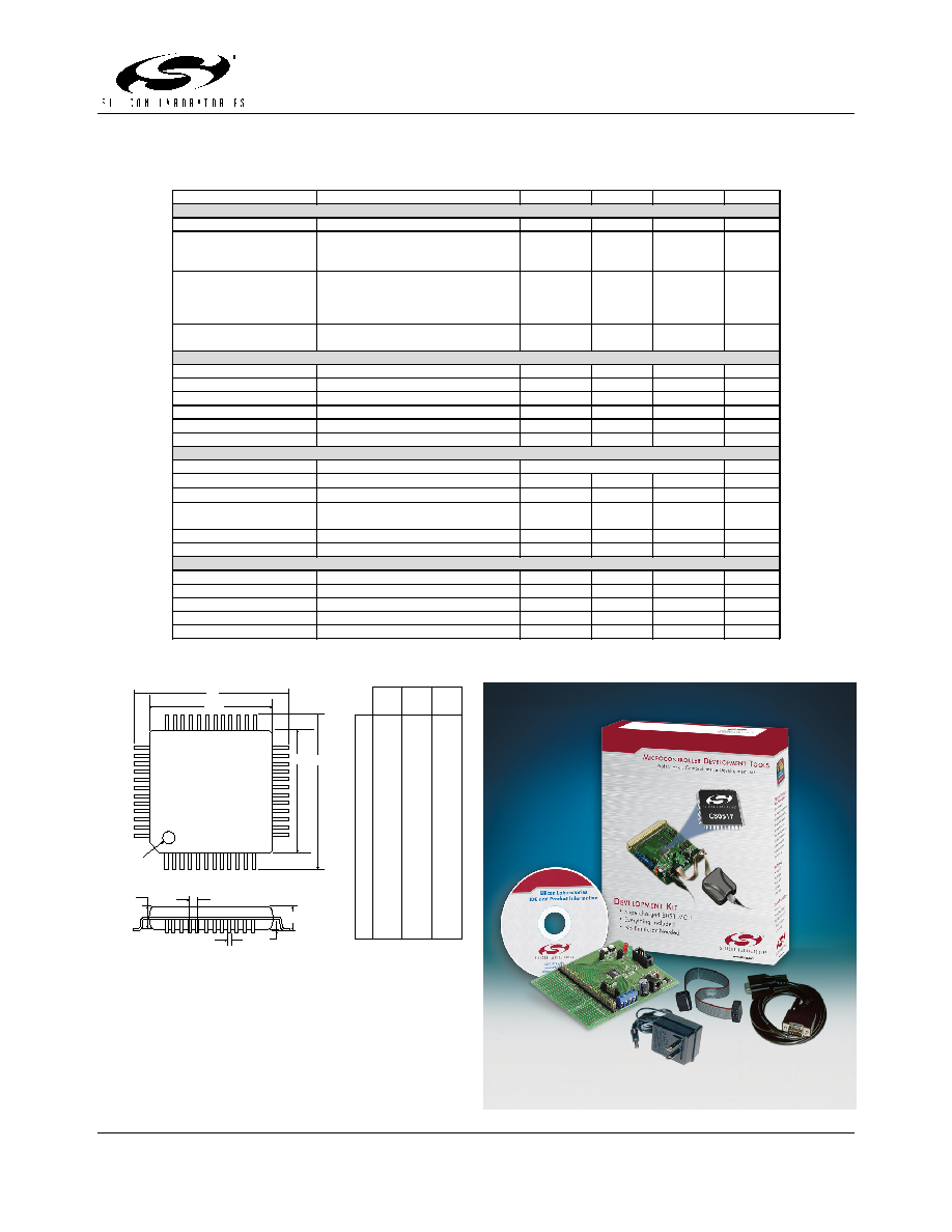
C8051F206DK Development Kit