Small Form Factor
Copyright © 2005 by Silicon Laboratories
4.8.2005
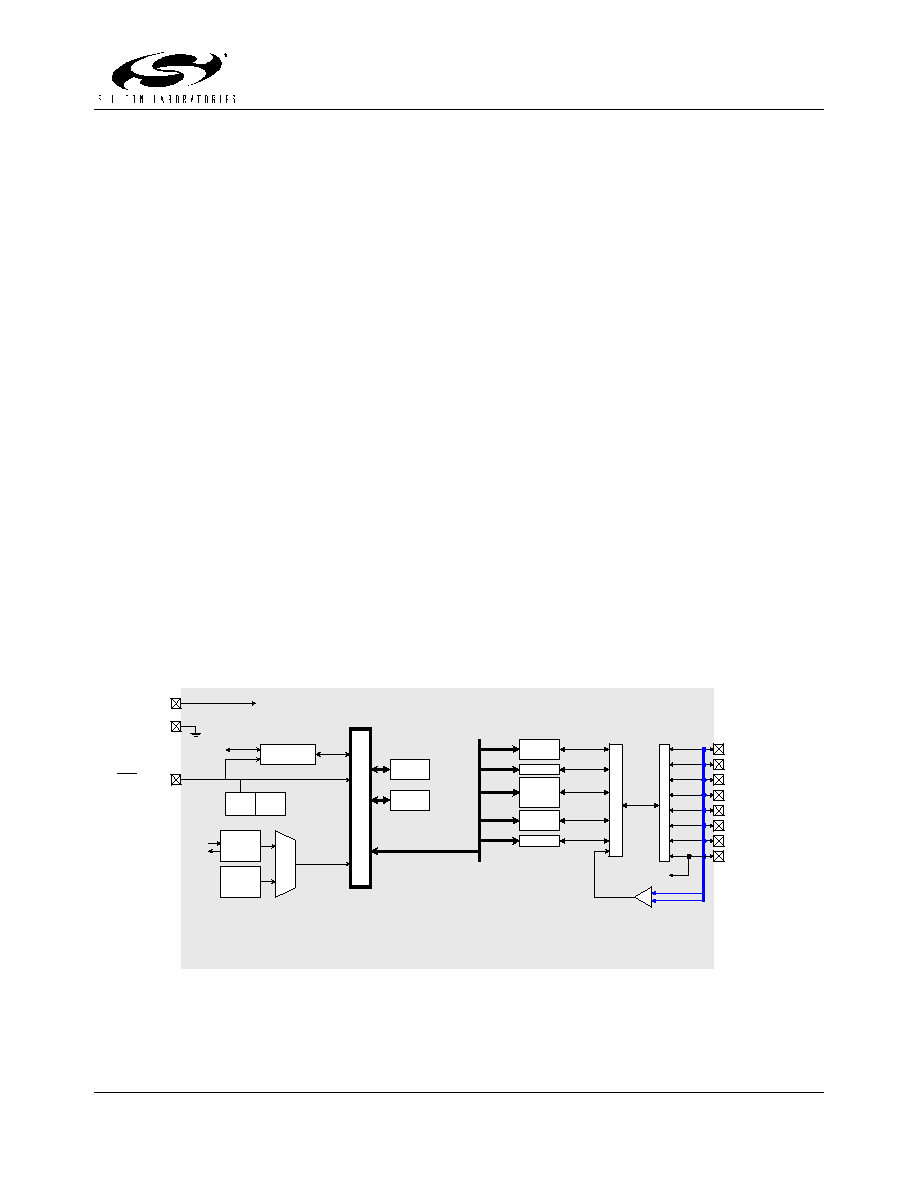
Port 0
Latch
UART
8 kB
FLASH
256 Byte
SRAM
POR
SFR Bus
8
0
5
1
C
o
r
e
Timer
0, 1, 2 /
RTC
PCA/
WDT
P
0
D
r
v
X
B
A
R
Reset
XTAL1
XTAL2
External
Oscillator
Circuit
System Clock
2%
Internal
Oscillator
Analog/Digital
Power
Debug HW
SMBus
C2D
C2D
CP0
+
-
P0.0
P0.1
P0.2/XTAL1
P0.3/XTAL2
P0.4/TX
P0.5/RX
P0.6/CNVST
P0.7/C2D
VDD
GND
RST/C2CK
Brown-
Out
C8051F301
25 MIPS, 8 kB Flash, 11-Pin Mixed-Signal MCU
Analog Peripherals
Comparator
-
Programmable hysteresis and response time
-
Configurable to generate interrupts or reset
-
Low current (0.4 µA)
POR/Brown-Out Detector
On-Chip Debug
-
On-chip debug circuitry facilitates full speed, non-intrusive in-system
debug (no emulator required)
-
Provides breakpoints, single stepping, watchpoints
-
Inspect/modify memory, registers, and stack
-
Superior performance to emulation systems using ICE-chips, target
pods, and sockets
Supply Voltage: 2.7 to 3.6 V
-
Typical operating current: 5.8 mA at 25 MHz
11 µA at 32 kHz
-
Typical stop mode current: <0.1 µA
Temperature Range: ≠40 to +85 ∞C
High-Speed 8051 µC Core
-
Pipelined Instruction architecture; executes 70% of instructions in 1 or 2
system clocks
-
Up to 25 MIPS throughput with 25 MHz clock
-
Expanded interrupt handler
Memory
-
256 bytes data RAM
-
8 kB Flash; in-system programmable in 512 byte sectors (512 bytes are
reserved)
Digital Peripherals
-
8 port I/O; all are 5 V tolerant
-
Enhanced Hardware SMBusTM (I2CTM compatible) and UART serial
ports
-
Programmable 16-bit counter/timer array with three capture/compare
modules, WDT
-
3 general-purpose 16-bit counter/timers
-
Dedicated watchdog timer; bidirectional reset
-
Real-time clock mode using PCA or timer and external clock source
Clock Sources
-
Internal oscillator: 25 MHz, 2% accuracy supports UART operation
-
External oscillator: Crystal, RC, C, or Clock (1 or 2 pin modes)
-
Can switch between clock sources on-the-fly
Package
-
11-pin MLP (Standard Lead and Lead-free packages)
Ordering Part Numbers
-
Lead-free package: C8051F301-GM
-
Standard package: C8051F301

Small Form Factor
Copyright © 2005 by Silicon Laboratories
4.8.2005
Silicon Laboratories and Silicon Labs are trademarks of Silicon Laboratories Inc.
Other products or brandnames mentioned herein are trademarks or registered trademarks of their respective holders
C8051F301
25 MIPS, 8 kB Flash, 11-Pin Mixed-Signal MCU
Selected Electrical Specifications
(T
A
= ≠40 to +85 C∞, VDD = 2.7 V unless otherwise specified)
PARAMETER CONDITIONS
MIN
TYP
MAX
UNITS
GLOBAL CHARACTERISTICS
Supply Voltage
2.7
3.6
V
Supply Current with
CPU active
Clock = 25 MHz
Clock = 1 MHz
Clock = 32 kHz; V
DD
Monitor Disabled
5.8
0.34
11
mA
mA
µA
Supply Current (shutdown)
Oscillator off; V
DD
Monitor Enabled
Oscillator off; V
DD
Monitor Disabled
10
<0.1
µA
µA
CPU & DIGITAL I/O PORTS
Clock Frequency Range
DC
25
MHz
Port Output High Voltage
I
OH
= -3 mA, Port I/O push-pull
V
DD
≠ 0.7
V
Port Output Low Voltage
I
OL
= 8.5 mA
0.6
V
Input High Voltage
0.7 x VDD
V
Input Low Voltage
0.3 x V
DD
V
INTERNAL OSCILLATOR
Frequency
24.0
24.5
25.0
MHz
COMPARATOR
Response Time Mode0
(CP+) ≠ (CP-) = 100 mV
0.1
µs
Current Consumption Mode0
7.6
µA
Response Time Mode1
(CP+) ≠ (CP-) = 100 mV
0.18
µs
Current Consumption Mode1
3.2
µA
Response Time Mode2
(CP+) ≠ (CP-) = 100 mV
0.32
µs
Current Consumption Mode2
1.3
µA
Response Time Mode3
(CP+) ≠ (CP-) = 100 mV
1
µs
Current Consumption Mode3
0.4
µA
Package Information
A
1
e
A3
A2
A
Side D View
Side E View
L
b
e
E
D
e
E2
D2
LT
LB
k
b
D4
Bottom View
R
e
A1
A
A3
A2
b
A3
A2
A1
A
k
L
LB
LT
R
D
D2
D3
E
E2
D4
e
0.18 0.23 0.30
0.25
0
0.65 1.00
0
0.02 0.05
0.80 0.90 1.00
MIN TYP MAX
0.27
0.45 0.55 0.65
0.36
0.37
0.09
3.00
0
2.20 2.25
2.27
3.00
1.36
0.386
0.5
MM
D3
C8051F300DK Development Kit