Rev. 1.0 5/05
Copyright � 2005 by Silicon Laboratories
Si2200
Si2200
RF S
Y N T H E S I Z E R
W I T H
I
N T E G R A T E D
VCO
S
F O R
S
A T E L L I T E
R
A D I O
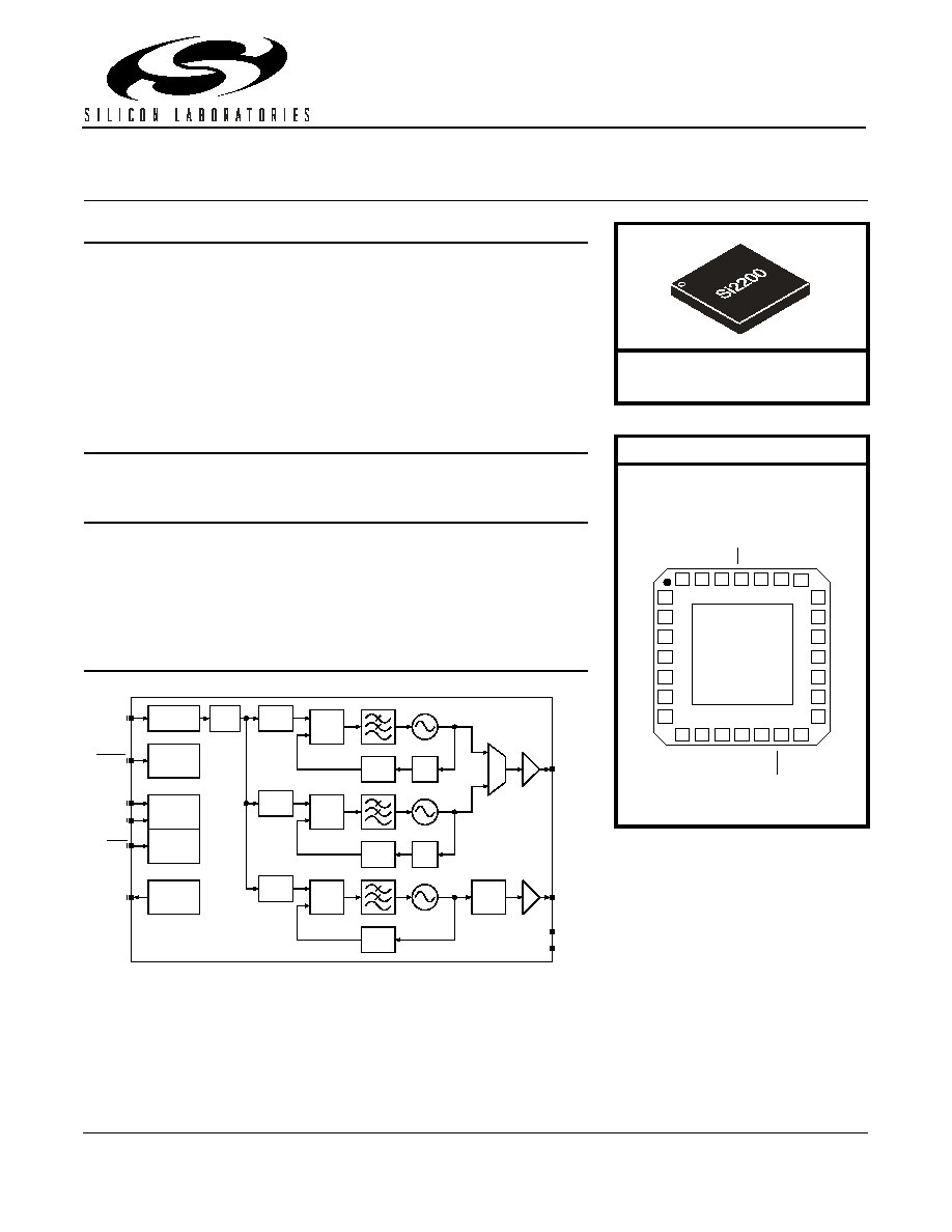
Features
Applications
Description
The Si2200 is a monolithic integrated circuit that performs both IF and RF
synthesis for wireless communications applications. The Si2200 includes
three VCOs, loop filters, reference and VCO dividers, and phase
detectors. Divider and powerdown settings are programmable through a
three-wire serial interface.
Functional Block Diagram
!
Dual-band RF synthesizers
"
RF1: 2300 to 2500 MHz
"
RF2: 2025 to 2300 MHz
!
IF synthesizer
"
62.5 to 1000 MHz
!
Integrated VCOs, loop filters,
varactors, and resonators
!
Minimal external components
required
!
Low phase noise
!
5 �A standby current
!
25.7 mA typical supply current
!
2.9 to 3.6 V operation
!
28-lead QFN
"
Lead-Free and RoHS Compliant
!
Satellite Radio
IFOUT
IFLA
IFLB
RFOUT
XIN
PWDN
SDATA
SCLK
SEN
IF
RF2
RF1
AUXOUT
Phase
Detect
Phase
Detect
�
2
�
2
IFDIV
Phase
Detect
Test
Mux
22-bit
Data
Register
Serial
Interface
Power
Down
Control
Reference
Amplifier
�
R
RF1
�
R
RF2
�
R
IF
�
N
RF1
�
N
RF2
�
N
IF
�1/�2
Patents pending
Ordering Information:
See page 28.
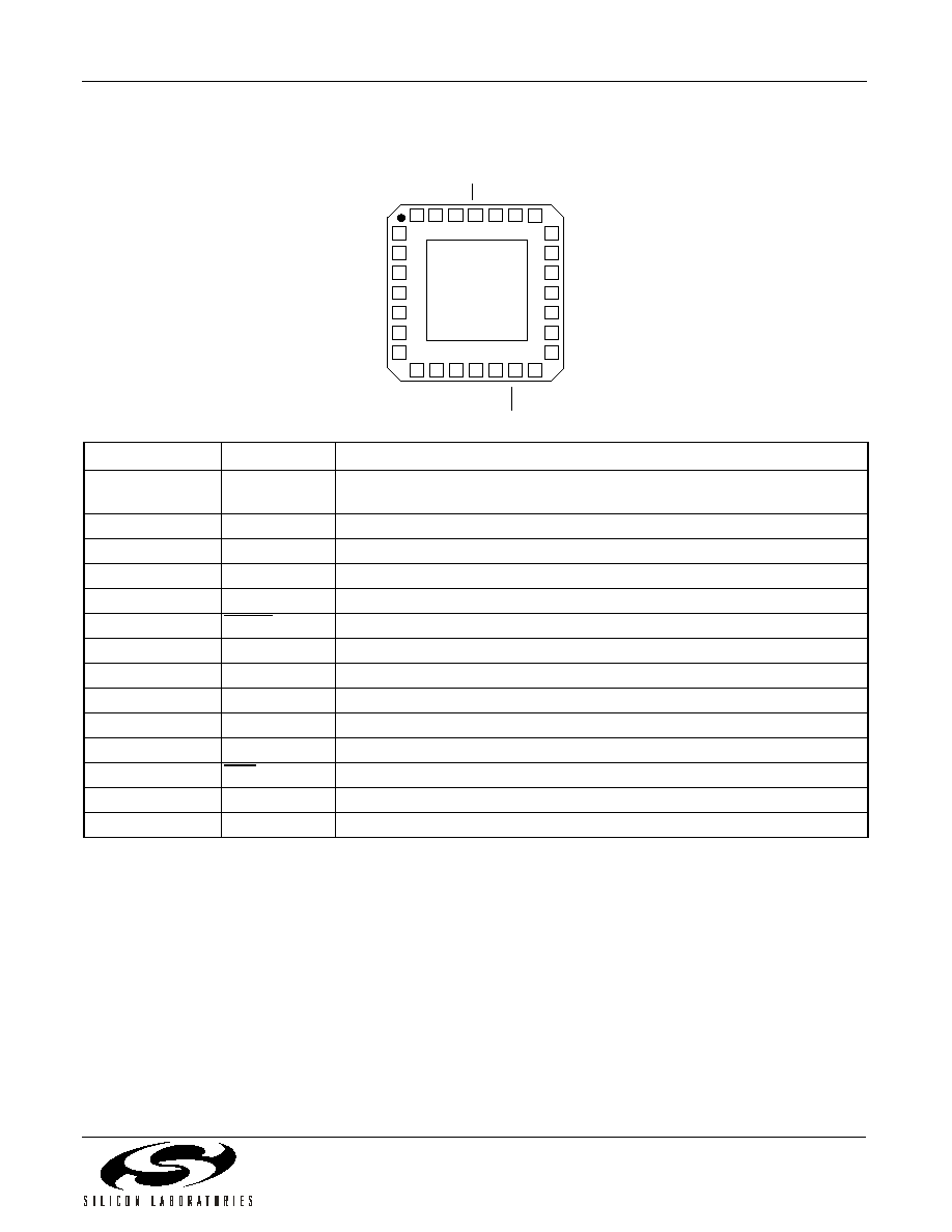
Pin Assignments
Si2200-GM
SC
L
K
SD
A
T
A
GN
D
GND
NC
NC
GND
GND
RFO
U
T
VD
D
R
SEN
VD
D
I
IFOU
T
GND
IFLB
IFLA
GN
D
VDDD
GND
XIN
PWD
N
AU
XOU
T
21
20
19
18
17
16
15
8
9
10 11 12 13 14
28 27 26 25 24 23 22
1
2
3
4
5
6
7
GN
D
GND
GND
GND
GND
GND
GND

Si2200
2
Rev. 1.0

Si2200
Rev. 1.0
3
T
A B L E
O F
C
O N T E N TS
Section
Page
1. Electrical Specifications . . . . . . . . . . . . . . . . . . . . . . . . . . . . . . . . . . . . . . . . . . . . . . . . . . .4
2. Functional Description . . . . . . . . . . . . . . . . . . . . . . . . . . . . . . . . . . . . . . . . . . . . . . . . . . .16
2.1. Serial Interface . . . . . . . . . . . . . . . . . . . . . . . . . . . . . . . . . . . . . . . . . . . . . . . . . . . . .16
2.2. Setting the IF VCO Center Frequencies . . . . . . . . . . . . . . . . . . . . . . . . . . . . . . . . . .16
2.3. Self-Tuning Algorithm . . . . . . . . . . . . . . . . . . . . . . . . . . . . . . . . . . . . . . . . . . . . . . . .17
2.4. Output Frequencies . . . . . . . . . . . . . . . . . . . . . . . . . . . . . . . . . . . . . . . . . . . . . . . . . .18
2.5. PLL Loop Dynamics . . . . . . . . . . . . . . . . . . . . . . . . . . . . . . . . . . . . . . . . . . . . . . . . .18
2.6. RF and IF Outputs (RFOUT and IFOUT) . . . . . . . . . . . . . . . . . . . . . . . . . . . . . . . . .18
2.7. Reference Frequency Amplifier . . . . . . . . . . . . . . . . . . . . . . . . . . . . . . . . . . . . . . . . .19
2.8. Powerdown Modes . . . . . . . . . . . . . . . . . . . . . . . . . . . . . . . . . . . . . . . . . . . . . . . . . .19
2.9. Auxiliary Output (AUXOUT) . . . . . . . . . . . . . . . . . . . . . . . . . . . . . . . . . . . . . . . . . . .19
3. Control Registers . . . . . . . . . . . . . . . . . . . . . . . . . . . . . . . . . . . . . . . . . . . . . . . . . . . . . . . .21
4. Pin Descriptions: Si2200 . . . . . . . . . . . . . . . . . . . . . . . . . . . . . . . . . . . . . . . . . . . . . . . . . .27
5. Ordering Guide . . . . . . . . . . . . . . . . . . . . . . . . . . . . . . . . . . . . . . . . . . . . . . . . . . . . . . . . . .28
6. Package Outline: Si2200-GM . . . . . . . . . . . . . . . . . . . . . . . . . . . . . . . . . . . . . . . . . . . . . . .29
Contact Information . . . . . . . . . . . . . . . . . . . . . . . . . . . . . . . . . . . . . . . . . . . . . . . . . . . . . . . .30
Si2200
4
Rev. 1.0
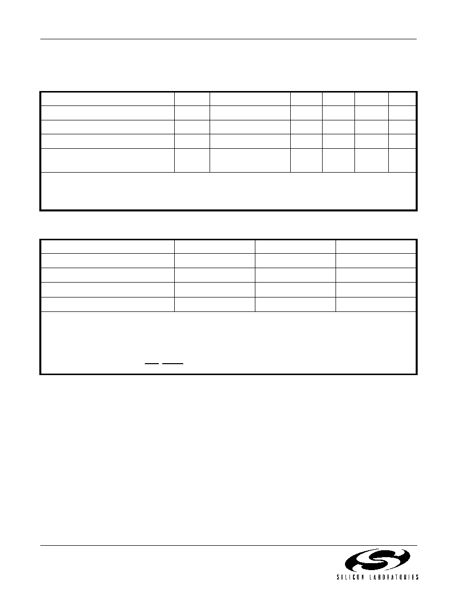
1. Electrical Specifications
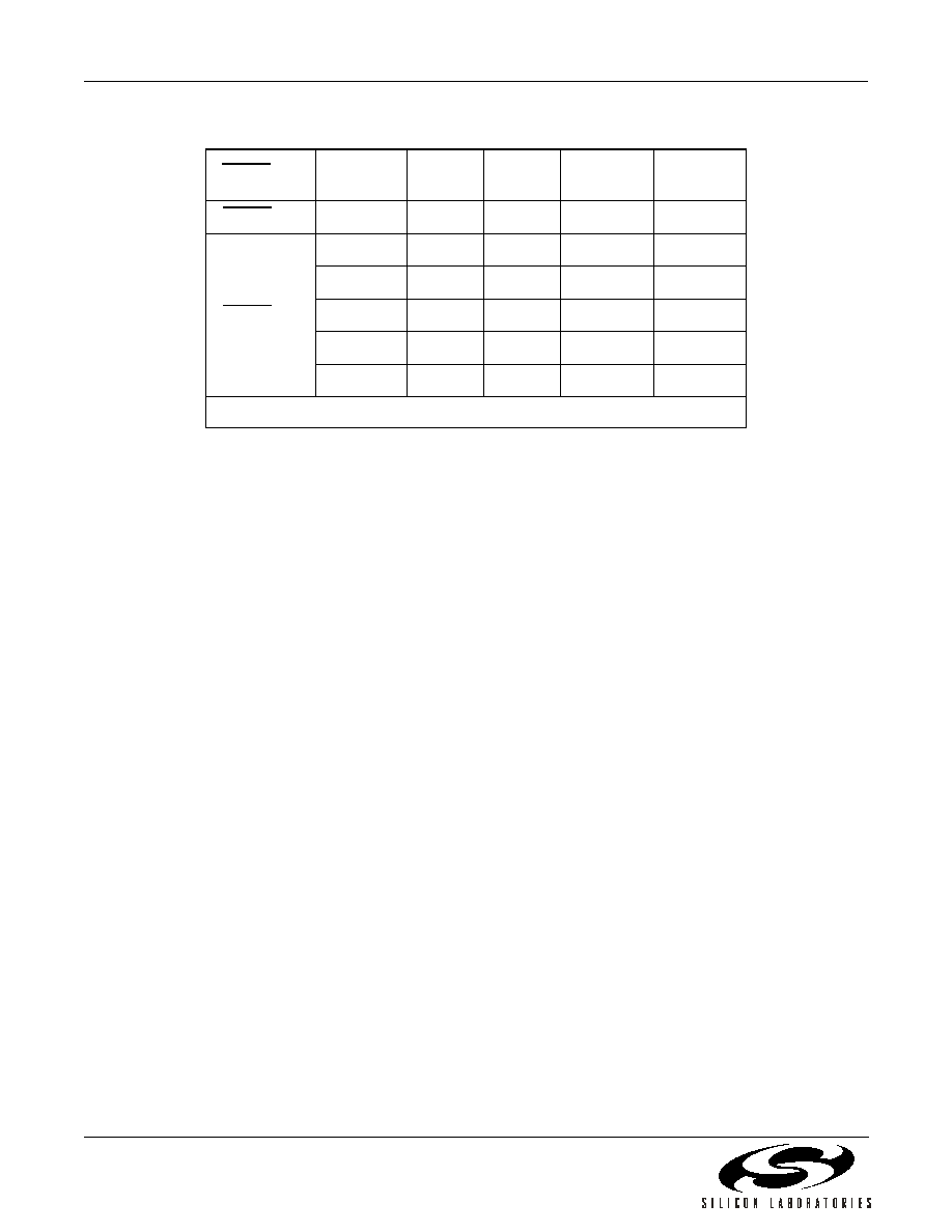
Table 1. Recommended Operating Conditions
1,2
Parameter
Symbol
Test Condition
Min
Typ
Max
Unit
Ambient Operating Temperature
T
A
�40
25
85
�C
Ambient Functional Temperature
T
F
�40
25
95
�C
Supply Voltage
V
DD
2.9
3.3
3.6
V
Supply Voltages Difference
V
(V
DDR
� V
DDD
),
(V
DDI
� V
DDD
)
�0.3
--
0.3
V
Notes:
1. All minimum and maximum specifications are guaranteed and apply across the recommended operating conditions.
Typical values apply at nominal supply voltages and an operating temperature of 25 �C unless otherwise stated.
2. Minimum and maximum specifications are not guaranteed across the functional temperature range.
Table 2. Absolute Maximum Ratings
1,2
Parameter
Symbol
Value
Unit
DC Supply Voltage
V
DD
�0.5 to 4.0
V
Input Current
3
I
IN
�10
mA
Input Voltage
3
V
IN
�0.3 to V
DD
+0.3
V
Storage Temperature Range
T
STG
�55 to 150
o
C
Notes:
1. Permanent device damage may occur if the above Absolute Maximum Ratings are exceeded. Functional operation
should be restricted to the conditions as specified in the operational sections of this data sheet. Exposure to absolute
maximum rating conditions for extended periods may affect device reliability.
2. This device is a high performance RF integrated circuit with an ESD rating of < 2 kV. Handling and assembly of this
device should only be done at ESD-protected workstations.
3. For signals SCLK, SDATA, SEN, PWDN, and XIN.
Si2200
Rev. 1.0
5
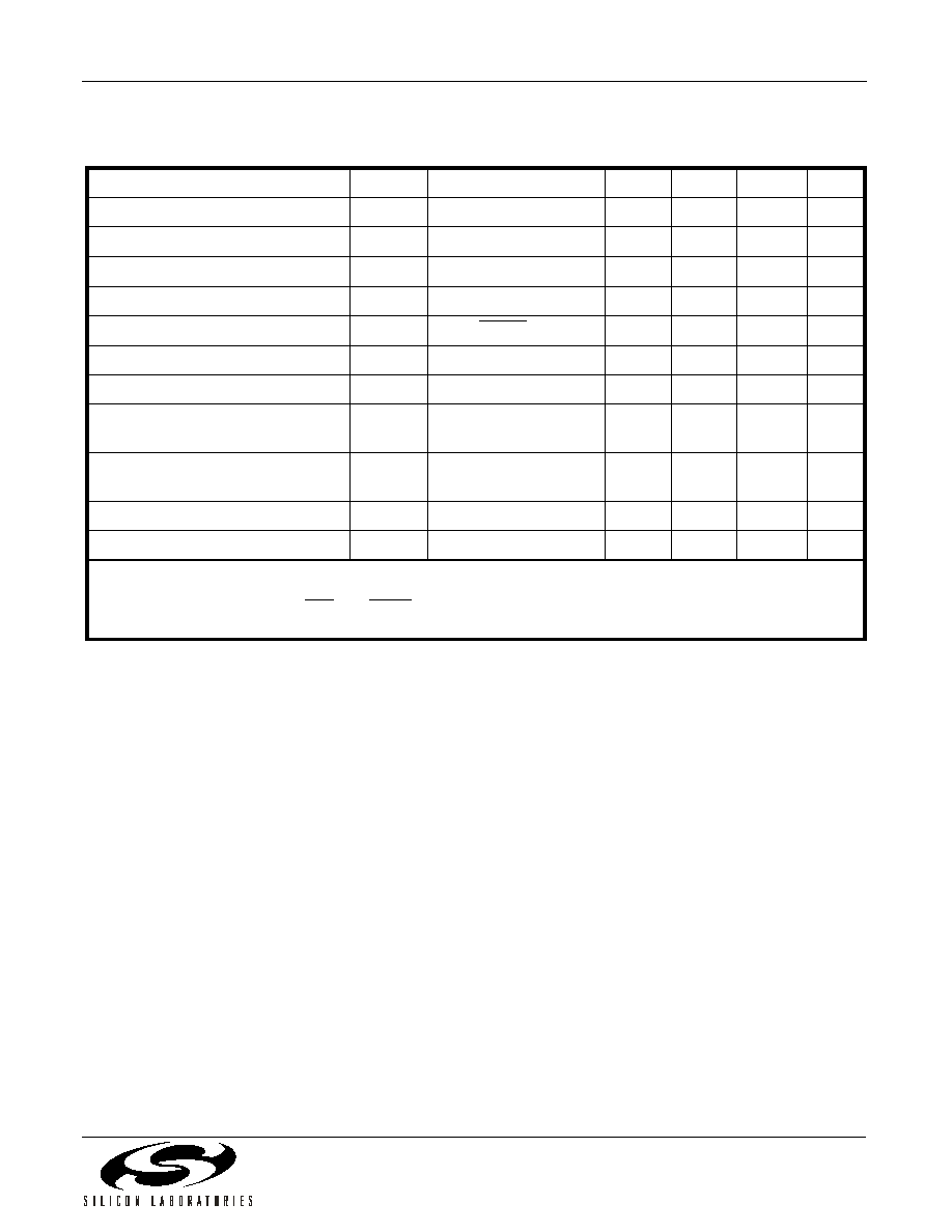
Table 3. DC Characteristics
(V
DD
= 2.7 to 3.6 V, T
A
= �40 to 85 �C)
Parameter
Symbol
Test Condition
Min
Typ
Max
Unit
Total Supply Current
1
RF1 and IF operating
--
28.7
35
mA
RF1 Mode Supply Current
1
--
19.5
24
mA
RF2 Mode Supply Current
1
--
18.5
23
mA
IF Mode Supply Current
1
--
10
12
mA
Standby Current
PWDN = 0
--
1
--
�A
High Level Input Voltage
2
V
IH
0.7 V
DD
--
--
V
Low Level Input Voltage
2
V
IL
--
--
0.3 V
DD
V
High Level Input Current
2
I
IH
V
IH
= 3.6 V,
V
DD
= 3.6 V
�10
--
10
�A
Low Level Input Current
2
I
IL
V
IL
= 0 V,
V
DD
=
3.6 V
�10
--
10
�A
High Level Output Voltage
3
V
OH
I
OH
= �500 �A
V
DD
�0.4
--
--
V
Low Level Output Voltage
3
V
OL
I
OH
= 500 �A
--
--
0.4
V
Notes:
1. RF1
=
2.4 GHz, RF2
=
2.1 GHz, IFOUT
=
800 MHz, LPWR
=
0.
2. For signals SCLK, SDATA, SEN, and PWDN.
3. For signal AUXOUT.
Si2200
6
Rev. 1.0
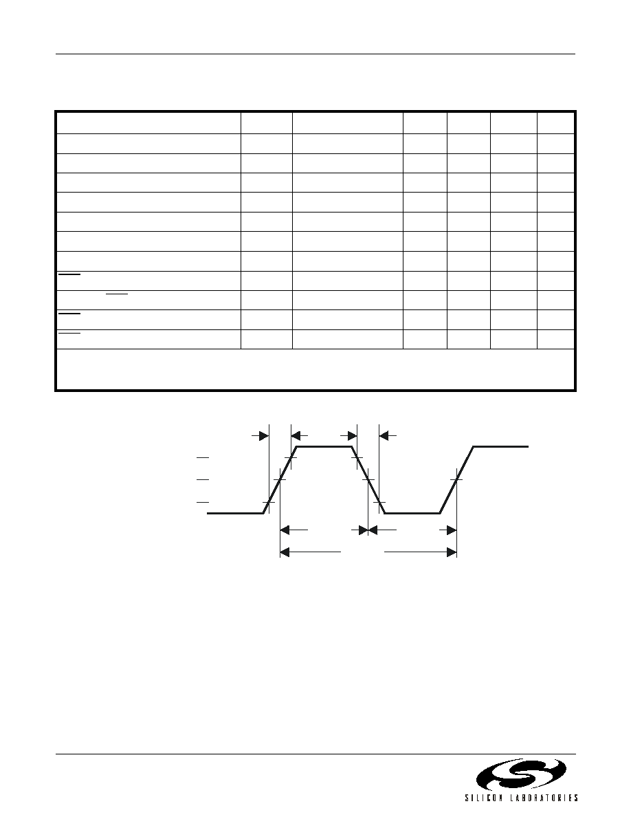
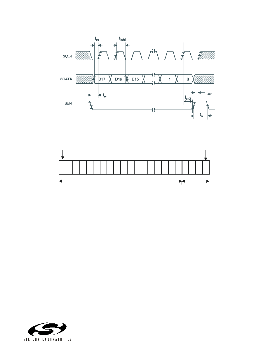
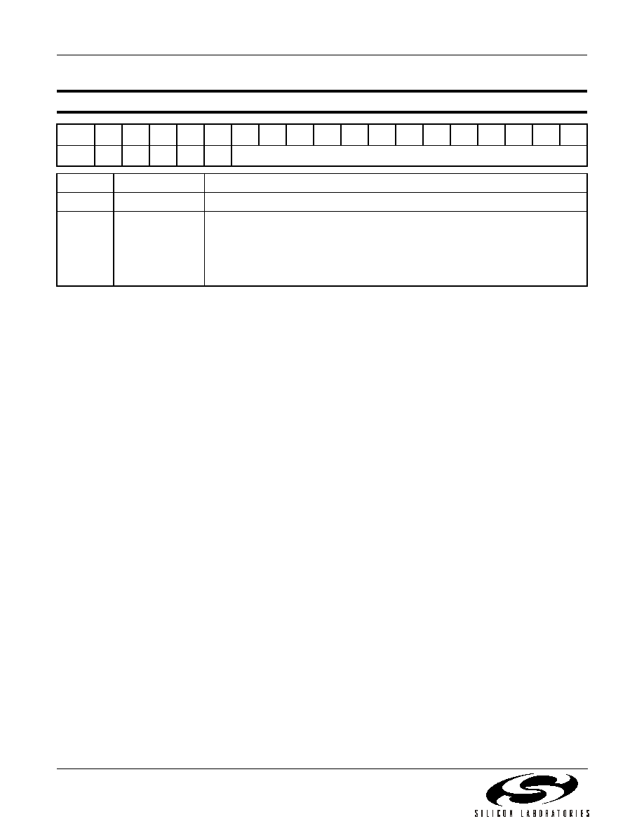
Figure 1. SCLK Timing Diagram
Table 4. Serial Interface Timing
(V
DD
= 2.7 to 3.6 V, T
A
= �40 to 85 �C)
Parameter
1
Symbol
Test Condition
Min
Typ
Max
Unit
SCLK Cycle Time
t
clk
Figure 1
40
--
--
ns
SCLK Rise Time
t
r
Figure 1
--
--
50
ns
SCLK Fall Time
t
f
Figure 1
--
--
50
ns
SCLK High Time
t
h
Figure 1
10
--
--
ns
SCLK Low Time
t
l
Figure 1
10
--
--
ns
SDATA Setup Time to SCLK
2
t
su
Figure 2
5
--
--
ns
SDATA Hold Time from SCLK
2
t
hold
Figure 2
0
--
--
ns
SEN
to SCLK
Delay Time
2
t
en1
Figure 2
10
--
--
ns
SCLK
to SEN
Delay Time
2
t
en2
Figure 2
12
--
--
ns
SEN
to SCLK
Delay Time
2
t
en3
Figure 2
12
--
--
ns
SEN Pulse Width
t
w
Figure 2
10
--
--
ns
Notes:
1. All timing is referenced to the 50% level of the waveform, unless otherwise noted.
2. Timing is not referenced to the 50% level of the waveform. See Figure 2.
SCLK
80%
50%
20%
t
r
t
f
t
h
t
l
t
clk
Si2200
Rev. 1.0
7
Figure 2. Serial Interface Timing Diagram
Figure 3. Serial Word Format
A
A
D
17
D
16
D
15
D
14
D
13
D
12
D
11
D
10
D
9
D
8
D
7
D
6
D
5
D
4
D
3
D
2
D
1
D
0
A
3
A
2
A
1
First bit
clocked in
Last bit
clocked in
address
field
A
0
data
field
Si2200
8
Rev. 1.0
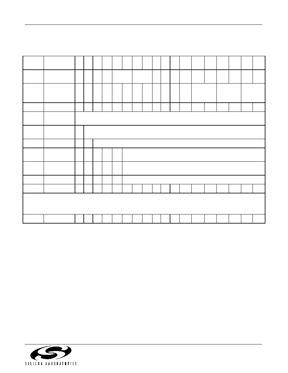
Table 5. RF and IF Synthesizer Characteristics
(V
DD
= 2.7
to 3.6 V, T
A
=
�40 to 85 �C)
Parameter
1
Symbol
Test Condition
Min
Typ
Max
Unit
XIN Input Frequency
f
REF
XINDIV2 = 0
2
--
25
MHz
XIN Input Frequency
f
REF
XINDIV2 = 1
25
--
50
MHz
Reference Amplifier Sensitivity
V
REF
0.5
--
V
DD
+0.3 V
V
PP
Phase Detector Update Frequency
f
f
= f
REF
/R for
XINDIV2 = 0
f
= f
REF
/2R for
XINDIV2 = 1
0.010
--
1.0
MHz
RF1 VCO Tuning Range
2
2300
--
2500
MHz
RF2 VCO Tuning Range
2
2025
--
2300
MHz
IF VCO Center Frequency Range
f
CEN
526
--
952
MHz
IFOUT Tuning Range from f
CEN
with IFDIV
62.5
--
1000
MHz
IFOUT VCO Tuning Range from f
CEN
Note: L �10%
�5
--
5
%
RF1 VCO Pushing
Open loop
--
0.75
--
MHz/V
RF2 VCO Pushing
--
0.65
--
MHz/V
IF VCO Pushing
--
0.10
--
MHz/V
RF1 VCO Pulling
VSWR = 2:1, all
phases, open loop
--
0.250
--
MHz p-p
RF2 VCO Pulling
--
0.100
--
MHz p-p
IF VCO Pulling
--
0.025
--
MHz p-p
RF1 Phase Noise
1 MHz offset
--
�130
--
dBc/Hz
RF1 Integrated Phase Error
100 Hz to 100 kHz
--
1.2
--
degrees
rms
RF2 Phase Noise
1 MHz offset
--
�131
--
dBc/Hz
RF2 Integrated Phase Error
100 Hz to 100 kHz
--
1.0
--
degrees
rms
IF Phase Noise at 800 MHz
100 kHz offset
--
�104
--
dBc/Hz
IF Integrated Phase Error
100 Hz to 100 kHz
--
0.4
--
degrees
rms
Notes:
1. f
(RF)
=
1 MHz, f
(IF)
=
1 MHz, RF1 = 2.4 GHz, RF2 = 2.1 GHz, IFOUT = 800 MHz, LPWR = 0.
2. RF VCO tuning range limits are fixed by inductance of internally bonded wires.
3. From powerup request (PWDN
or SEN
during a write of 1 to bits PDIB and PDRB in Register 2) to RF and IF
synthesizers ready (settled to within 0.1 ppm frequency error).
4. From powerdown request (PWDN
, or SEN
during a write of 0 to bits PDIB and PDRB in Register 2) to supply current
equal to I
PWDN
.
Si2200
Rev. 1.0
9
RF1 Harmonic Suppression
Second Harmonic
--
�28
�20
dBc
RF2 Harmonic Suppression
--
�23
�20
dBc
IF Harmonic Suppression
--
�26
�20
dBc
RFOUT Power Level
Z
L
= 50
,
RF1 active
�3
�1
3
dBm
RFOUT Power Level
Z
L
= 50
,
RF2 active
�3
�1
3
dBm
IFOUT Power Level
Z
L
= 50
�8
�4
0
dBm
RF1 Output Reference Spurs
Offset = 1 MHz
--
�63
--
dBc
Offset = 2 MHz
--
�68
--
dBc
Offset = 3 MHz
--
�70
--
dBc
RF2 Output Reference Spurs
Offset = 1 MHz
--
�63
--
dBc
Offset = 2 MHz
--
�68
--
dBc
Offset = 3 MHz
--
�70
--
dBc
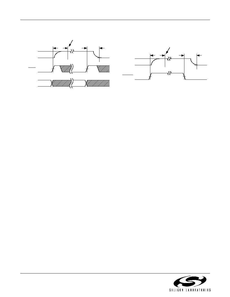
Powerup Request to Synthesizer Ready
3
Time
t
pup
Figures 4, 5
f
> 500 kHz
--
80
100
�s
Powerup Request to Synthesizer Ready
3
Time
t
pup
Figures 4, 5
f
500 kHz
--
40/f
50/f
Powerdown Request to Synthesizer Off
4
Time
t
pdn
Figures 4, 5
--
--
100
ns
Table 5. RF and IF Synthesizer Characteristics (Continued)
(V
DD
= 2.7
to 3.6 V, T
A
=
�40 to 85 �C)
Parameter
1
Symbol
Test Condition
Min
Typ
Max
Unit
Notes:
1. f
(RF)
=
1 MHz, f
(IF)
=
1 MHz, RF1 = 2.4 GHz, RF2 = 2.1 GHz, IFOUT = 800 MHz, LPWR = 0.
2. RF VCO tuning range limits are fixed by inductance of internally bonded wires.
3. From powerup request (PWDN
or SEN
during a write of 1 to bits PDIB and PDRB in Register 2) to RF and IF
synthesizers ready (settled to within 0.1 ppm frequency error).
4. From powerdown request (PWDN
, or SEN
during a write of 0 to bits PDIB and PDRB in Register 2) to supply current
equal to I
PWDN
.
Si2200
10
Rev. 1.0
Figure 4. Software Power Management
Timing Diagram
Figure 5. Hardware Power Management
Timing Diagram
PDIB = 0
PDRB = 0
PDIB = 1
PDRB = 1
t
pup
t
pdn
I
T
I
PWDN
SEN
SDATA
RF synthesizers settled to within
0.1 ppm frequency error.
t
pup
t
pdn
I
T
I
PWDN
PWDN
RF synthesizers settled to within
0.1 ppm frequency error.
Si2200
Rev. 1.0
11
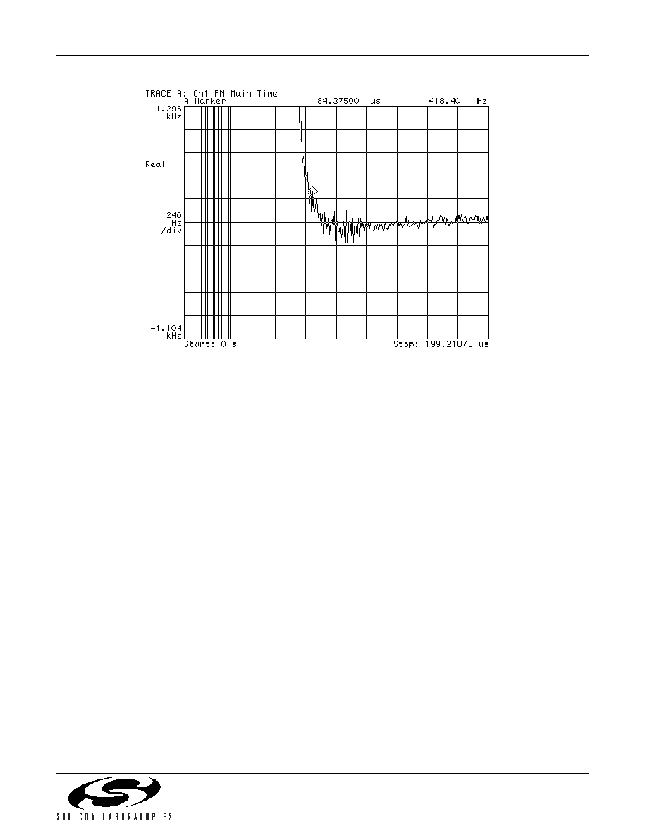
Figure 6. Typical Transient Response RF1 at 2.4 GHz
with 1 MHz Phase Detector Update Frequency
Si2200
12
Rev. 1.0
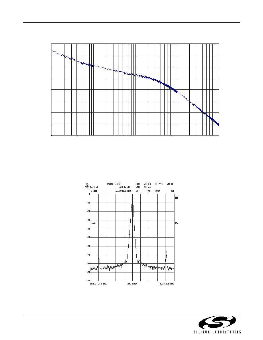
Figure 7. Typical RF1 Phase Noise at 2.4 GHz
with 1 MHz Phase Detector Update Frequency
Figure 8. Typical RF1 Spurious Response at 2.4 GHz
with 1 MHz Phase Detector Update Frequency
Typical RF1 Phase Noise at 2.4 GHz
-140
-130
-120
-110
-100
-90
-80
-70
-60
1.E+02
1.E+03
1.E+04
1.E+05
1.E+06
Offset Frequency (Hz)
P
hase No
i
s
e (dB
c
/
H
z
)
Si2200
Rev. 1.0
13
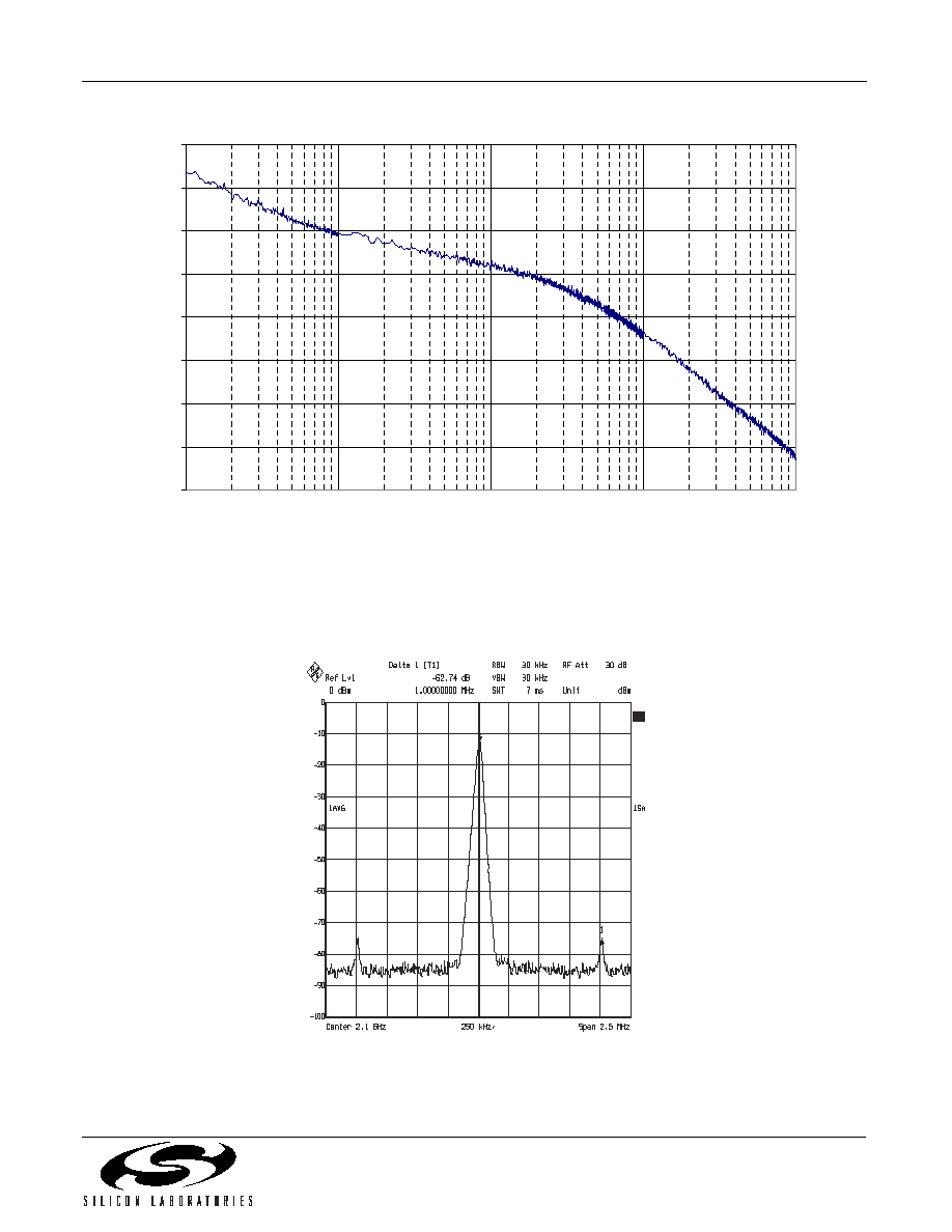
Figure 9. Typical RF2 Phase Noise at 2.1 GHz
with 1 MHz Phase Detector Update Frequency
Figure 10. Typical RF2 Spurious Response at 2.1 GHz
with 1 MHz Phase Detector Update Frequency
Typical RF2 Phase Noise at 2.1 GHz
-140
-130
-120
-110
-100
-90
-80
-70
-60
1.E+02
1.E+03
1.E+04
1.E+05
1.E+06
Offset Frequency (Hz)
P
hase Noise (dB
c
/Hz)
Si2200
14
Rev. 1.0
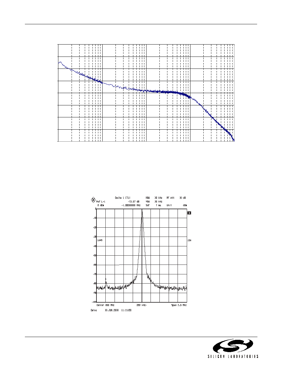
Figure 11. Typical IF Phase Noise at 800 MHz
with 1 MHz Phase Detector Update Frequency
Figure 12. IF Spurious Response at 800 MHz
with 1 MHz Phase Detector Update Frequency
Typical IF Phase Noise at 800 MHz
-140
-130
-120
-110
-100
-90
-80
-70
-60
1.E+02
1.E+03
1.E+04
1.E+05
1.E+06
Offset Frequency (Hz)
Phas
e N
o
i
s
e (
d
Bc
/H
z
)
Si2200
Rev. 1.0
15
Figure 13. Typical Application Circuit: Si2200
Si2200
RFOUT
560 pF
Printed Trace
Inductor or
Chip Inductor
IFOUT
560 pF
L
MATCH
From
System
Controller
V
DD
*Add 30
series resistor if using IF output divide values 2, 4, or 8 and f
CEN
< 600 MHz.
GN
D
RFO
U
T
V
DDR
GND
IFLB
IFLA
GND
VDDD
GND
XIN
AUX
O
U
T
1
2
3
4
5
6
7
8
9
10
11
12
21
20
19
18
17
16
15
14
13
GN
D
PW
D
N
GN
D
28
27
26
25
24
22
23
0.022
�
F
External
Clock
560 pF
PWDN
AUXOUT
V
DD
0.022
�
F
V
DD
0.022
�
F
30
GND
GND
NC
GND
NC
GND
GND
SC
L
K
S
DATA
V
DDI
IF
OU
T
GN
D
GN
D
SEN

Si2200
16
Rev. 1.0
2. Functional Description
The Si2200 is a monolithic integrated circuit that
performs IF and dual-band RF synthesis for many
wireless communications applications. This integrated
circuit (IC), along with a minimum number of external
components, is all that is necessary to implement the
frequency synthesis function in applications, such as
satellite radio.
The Si2200 has three complete phase-locked loops
(PLLs) with integrated voltage-controlled oscillators
(VCOs). The low phase noise of the VCOs makes the
Si2200 suitable for use in demanding wireless
communications applications. Also integrated are phase
detectors, loop filters, and reference and output
frequency dividers. The IC is programmed through a
three-wire serial interface.
Two PLLs are provided for RF synthesis. These RF
PLLs are multiplexed so that only one PLL is active at a
given time (as determined by the setting of an internal
register). The active PLL is the last one written. The
center frequency of the VCO in each PLL is set by the
internal bond wire inductance within the package.
Inaccuracies in these inductances are compensated for
by the self-tuning algorithm. The algorithm is run
following power-up or following a change in the
programmed output frequency.
The RF PLLs contain a divide-by-2 circuit before the N-
divider. As a result, the phase detector frequency (f
) is
equal to half the desired channel spacing. For example,
for a 200 kHz channel spacing, f
would equal 100 kHz.
The IF PLL does not contain the divide-by-2 circuit
before the N-divider. In this case, f
is equal to the
desired channel spacing. Each RF VCO is optimized for
a particular frequency range. The RF1 VCO is optimized
to operate from 2.3 to 2.5 GHz, while the RF2 VCO is
optimized to operate between 2.025 and 2.3 GHz.
One PLL is provided for IF synthesis. The center
frequency of this circuit's VCO is set by an external
inductance. The PLL can adjust the IF output frequency
by �5% of the VCO center frequency. Inaccuracies in
the value of the external inductance are compensated
for by the Si2200's proprietary self-tuning algorithm.
This algorithm is initiated each time the PLL is powered-
up (by either the PWDN pin or by software) and/or each
time a new output frequency is programmed. The IF
VCO can have its center frequency set as low as
526 MHz and as high as 952 MHz. An IF output divider
is provided to divide down the IF output frequencies, if
needed. The divider is programmable and capable of
dividing by 1, 2, 4, or 8.
In order to accommodate designs running at XIN
frequencies greater than 25 MHz, the Si2200 includes a
programmable divide-by-2 option (XINDIV2 in
Register 0, D6) on the XIN input. By enabling this
option, the Si2200 can accept a range of TCXO
frequencies from 25 to 50 MHz.
The unique PLL architecture used in the Si2200
produces settling (lock) times that are comparable in
speed to fractional-N architectures without suffering the
high phase noise or spurious modulation effects often
associated with those designs.
2.1. Serial Interface
A timing diagram for the serial interface is shown in
Figure 2 on page 7. Figure 3 on page 7 shows the
format of the serial word.
The Si2200 is programmed serially with 22-bit words
comprised of 18-bit data fields and 4-bit address fields.
When the serial interface is enabled (i.e., when SEN is
low) data and address bits on the SDATA pin are
clocked into an internal shift register on the rising edge
of SCLK. Data in the shift register is then transferred on
the rising edge of SEN into the internal data register
addressed in the address field. The serial interface is
disabled when SEN is high.
Table 11 on page 21 summarizes the data register
functions and addresses. It is not necessary (although it
is permissible) to clock into the internal shift register any
leading bits that are "don't cares."
2.2. Setting the IF VCO Center Frequencies
The IF PLL can adjust its output frequency �5% from
the center frequency as established by the value of an
external inductance connected to the VCO. The RF1
and RF2 PLLs have fixed operating ranges due to the
inductance set by the internal bond wires. Each center
frequency is established by the value of the total
inductance (internal and/or external) connected to the
respective VCO. Manufacturing tolerance of �10% for
the external inductor is acceptable for the IF VCO. The
Si2200 will compensate for inaccuracies by executing a
self-tuning algorithm following PLL power-up or
following a change in the programmed output
frequency.
Because the total tank inductance is in the low nH
range, the inductance of the package needs to be
considered in determining the correct external
inductance. The total inductance (L
TOT
) presented to
the IF VCO is the sum of the external inductance (L
EXT
)
and the package inductance (L
PKG
). The IF VCO has a
nominal capacitance (C
NOM
) in parallel with the total
inductance, and the center frequency is as follows:
Si2200
Rev. 1.0
17
Table 6 summarizes the characteristics of the IF VCO.
Figure 14. Example of IF External Inductor
As a design example, suppose synthesizing
frequencies in a 30 MHz band between 735 and
765 MHz is desired. The center frequency should be
defined as midway between the two extremes, or
750 MHz. The PLL will be able to adjust the VCO output
frequency �5% of the center frequency, or �37.5 MHz of
750 MHz (i.e., from approximately 713 to 788 MHz).
The IF VCO has a C
NOM
of 6.5 pF, and a 6.9 nH
inductance (correct to two digits) in parallel with this
capacitance will yield the desired center frequency. An
external inductance of 4.8 nH should be connected
between IFLA and IFLB, as shown in Figure 14. This, in
addition to 2.1 nH of package inductance, will present
the correct total inductance to the VCO. In
manufacturing, the external inductance can vary �10%
of its nominal value, and the Si2200 will correct for the
variation with the self-tuning algorithm.
For more information on designing the external trace
inductor, please refer to "AN31: Inductor Design for the
Si41xx Synthesizer Family".
2.3. Self-Tuning Algorithm
The self-tuning algorithm is initiated immediately
following power-up of a PLL or, if the PLL is already
powered, following a change in its programmed output
frequency. This algorithm attempts to tune the VCO so
that its free-running frequency is near the desired output
frequency. In so doing, the algorithm will compensate
for manufacturing tolerance errors in the value of the
external inductance connected to the IF VCO. It will also
reduce the frequency error for which the PLL must
correct to get the precise desired output frequency. The
self-tuning algorithm will leave the VCO oscillating at a
frequency in error by somewhat less than 1% of the
desired output frequency.
After self-tuning, the PLL controls the VCO oscillation
frequency. The PLL will complete frequency locking,
eliminating any remaining frequency error. Thereafter, it
will maintain frequency-lock, compensating for effects
caused by temperature and supply voltage variations.
The Si2200's self-tuning algorithm will compensate for
component value errors at any temperature within the
specified temperature range. However, the ability of the
PLL to compensate for drift in component values that
occur after self-tuning is limited. For external
inductances with temperature coefficients around
�150 ppm/�C, the PLL will be able to maintain lock for
changes in temperature of approximately �30 �C.
Applications where the PLL is regularly powered-down
or the frequency is periodically reprogrammed minimize
or eliminate the potential effects of temperature drift
because the VCO is re-tuned in either case. In
applications where the ambient temperature can drift
substantially after self-tuning, it may be necessary to
monitor the lock-detect bar (LDETB) signal on the
AUXOUT pin to determine whether a PLL is about to
run out of locking capability. (See "Auxiliary Output
(AUXOUT)" for how to select LDETB.) The LDETB
signal will be low after self-tuning has completed but will
rise when either the IF or RF PLL nears the limit of its
compensation range. (LDETB will also be high when
either PLL is executing the self-tuning algorithm.) The
output frequency will still be locked when LDETB goes
high, but the PLL will eventually lose lock if the
temperature continues to drift in the same direction.
Therefore, if LDETB goes high both the IF and RF PLLs
should promptly be retuned by initiating the self-tuning
algorithm.
Table 6. Si2200-GM VCO Characteristics
VCO
F
CEN
Range
(MHz)
C
NOM
(pF)
L
PKG
(nH)
L
EXT
Range
(nH)
Min
Max
Min
Max
IF
526
952
6.5
2.1
2.2
12.0
f
CEN
1
2
L
TOT
C
NOM
�
-----------------------------------------------
1
2
L
PKG
L
EXT
+
(
)
C
NOM
�
------------------------------------------------------------------------
=
=
Si4136XM
L
PKG
2
L
PKG
2
L
EXT
IFLB
IFLA
Si2200
18
Rev. 1.0
2.4. Output Frequencies
The IF and RF output frequencies are set by
programming the R- and N-Divider registers. Each PLL
has its own R and N registers so that each can be
programmed independently. Programming either the R-
or N-Divider register for RF1 or RF2 automatically
selects the associated output.
When XINDIV2 = 0, the reference frequency on the XIN
pin is divided by R, and this signal is the input to the
PLL's phase detector. The other input to the phase
detector is the PLL's VCO output frequency divided by
2N for the RF PLLs or N for the IF PLL. After an initial
transient:
Equation 1. f
OUT
= (2N/R)
"
f
REF
(for the RF
PLLs)
Equation 2. f
OUT
= (N/R)
"
f
REF
(for the IF PLL).
The integers R are set by programming the RF1 R-
Divider register (Register 6), the RF2
R-Divider register
(Register 7) and the IF R-Divider register (Register 8).
The integers N are set by programming the RF1 N-
Divider register (register 3), the RF2 N-Divider register
(Register 4), and the IF N-Divider register (Register 5).
If the optional divide-by-2 circuit on the XIN pin is
enabled (XINDIV2 = 1), after an initial transient:
f
OUT
= (N/R)
"
f
REF
(for the RF PLLs)
f
OUT
= (N/2R)
"
f
REF
(for the IF PLL).
Each N-Divider is implemented as a conventional high-
speed divider. That is, it consists of a dual-modulus
prescaler, a swallow counter, and a lower speed
synchronous counter. However, the control of these
sub-circuits is handled automatically. Only the
appropriate N value should be programmed.
2.5. PLL Loop Dynamics
The transient response for each PLL is determined by
its phase detector update rate f
(equal to f
REF
/R) and
the phase detector gain programmed for each RF1,
RF2, or IF synthesizer. (See Register 1.) Four different
settings for the phase detector gain are available for
each PLL. The highest gain is programmed by setting
the two phase detector gain bits to 00 and the lowest by
setting the bits to 11. The values of the available gains,
relative to the highest gain, are listed in Table 7.
In general, a higher phase detector gain will decrease
in-band phase noise and increase the speed of the PLL
transient until the point at which stability begins to be
compromised. The optimal gain depends on N. Table 8
lists recommended settings for different values of N.
The VCO gain and loop filter characteristics are not
programmable.
The settling time for each PLL is directly proportional to
its phase detector update period T
(T
equals 1/f
).
During the first 13 update periods, the Si2200 executes
the self-tuning algorithm. Thereafter, the PLL controls
the output frequency. Because of the unique
architecture of the Si2200 PLLs, the time required to
settle the output frequency to 0.1 ppm error is only
about 25 update periods. Thus, the total time after
power-up or a change in programmed frequency until
the synthesized frequency is well settled--including
time for self-tuning--is around 40 update periods.
Note:
This settling time analysis holds for f
500 kHz
. For
f
>
500 kHz
, the settling time can be a maximum of
100
�
s as specified in Table 5.
2.6. RF and IF Outputs (RFOUT and IFOUT)
The RFOUT and IFOUT pins are driven by amplifiers
that buffer the RF VCOs and IF VCO, respectively. The
RF output amplifier receives its input from either the
RF1 or RF2 VCO, depending upon which R- or N-
Divider register was last written. For example,
programming the N-Divider register for RF1
automatically selects the RF1 VCO output.
Table 7. Gain Values (Register 1)
K
P
Bits
Relative P.D.
Gain
00
1
01
1/2
10
1/4
11
1/8
Table 8. Optimal K
P
Settings
N
RF1
K
P1
<1:0>
RF2
K
P2
<1:0>
IF
K
PI
<1:0>
2047
00
00
00
2048 to 4095
00
01
01
4096 to 8191
01
10
10
8192 to 16383
10
11
11
16384
11
11
11
Table 7. Gain Values (Register 1)
K
P
Bits
Relative P.D.
Gain
Si2200
Rev. 1.0
19
Figure 13 on page 15 shows an application diagram for
the Si2200. The RF output signal must be ac-coupled to
its load through a capacitor.
The IFOUT pin must also be ac-coupled to its load
through a capacitor. The IF output level is dependent
upon the load. Figure 17 displays the output level
versus load resistance. For resistive loads greater than
500
, the output level saturates, and the bias currents
in the IF output amplifier are higher than they need to
be. The LPWR bit in the Main Configuration register
(Register 0) can be set to 1 to reduce the bias currents
and, therefore, reduce the power dissipated by the IF
amplifier. For loads less than 500
,
LPWR should be
set to 0 to maximize the output level.
For IF frequencies greater than 500 MHz, a matching
network is required in order to drive a 50
load. See
Figure 15 below. The value of L
MATCH
can be
determined by Table 9.
Typical values range between 8 nH and 40 nH.
Figure 15. IF Frequencies > 500 MHz
For frequencies less than 500 MHz, the IF output buffer
can directly drive a 200
resistive load or higher. For
resistive loads greater than 500
(f < 500 MHz) the
LPWR bit can be set to reduce the power consumed by
the IF output buffer. See Figure 16 below.
Figure 16. IF Frequencies < 500 MHz
Figure 17. Typical IF Output Voltage vs.
Load Resistance at 550 MHz
2.7. Reference Frequency Amplifier
The Si2200 provides a reference frequency amplifier. If
the driving signal has CMOS levels, it can be connected
directly to the XIN pin. Otherwise, the reference
frequency signal should be ac coupled to the XIN pin
through a 560 pF capacitor.
2.8. Powerdown Modes
Table 10 summarizes the powerdown functionality. The
Si2200 can be powered down by taking the PWDN pin
low or by setting bits in the Powerdown register
(Register 2). When the PWDN pin is low, the Si2200 will
be powered down regardless of the Powerdown register
settings. When the PWDN pin is high, power
management is under control of the Powerdown register
bits.
The IF and RF sections of the Si2200 circuitry can be
individually powered down by setting the Powerdown
register bits, PDIB and PDRB, low. The reference
frequency amplifier will also be powered up if either the
PDRB or PDIB bits are high. Also, setting the
AUTOPDB bit to 1 in the Main Configuration register
(Register 0) is equivalent to setting both bits in the
Powerdown register to 1.
The serial interface remains available and can be
written in all power-down modes.
2.9. Auxiliary Output (AUXOUT)
The signal appearing on AUXOUT is selected by setting
the AUXSEL bits in the Main Configuration register
(Register 0).
The LDETB signal can be selected by setting the
AUXSEL bits to 011. This signal can be used to indicate
that the IF or RF PLL is about to lose lock due to
excessive ambient temperature drift and should be re-
tuned.
Table 9. L
MATCH
Values
Frequency
L
MATCH
500�600 MHz
40 nH
600�800 MHz
27 nH
800�1 GHz
18 nH
IFOUT
L
MATCH
>500 pF
50
IFOUT
>500 pF
>200
0
50
100
150
200
250
300
350
400
450
0
200
400
600
800
1000
1200
Load Resistance (
)
Output Voltage (mVrms)
LPWR=0
LPWR=1
Si2200
20
Rev. 1.0
Table 10. Powerdown Configuration
PWDN Pin
AUTOPDB
PDIB
PDRB
IF Circuitry
RF
Circuitry
PWDN = 0
x
x
x
OFF
OFF
PWDN = 1
0
0
0
OFF
OFF
0
0
1
OFF
ON
0
1
0
ON
OFF
0
1
1
ON
ON
1
x
x
ON
ON
Note:
x
=
don't care.
Si2200
Rev. 1.0
21
3. Control Registers
Note:
Registers 9�15 are reserved. Writes to these registers may result in unpredictable behavior.
Table 11. Register Summary
Register Name
Bit
17
Bit
16
Bit
15
Bit
14
Bit
13
Bit
12
Bit
11
Bit
10
Bit
9
Bit
8
Bit
7
Bit
6
Bit
5
Bit
4
Bit
3
Bit
2
Bit
1
Bit
0
0
Main
Configuration
0
0
0
0
AUXSEL
IFDIV
1
1
0
XIN
DIV2
LPWR
0
AUTO
PDB
0
1
0
1
Phase
Detector
Gain
0
0
0
0
0
0
0
0
0
0
0
0
K
PI
K
P2
K
P1
2
Powerdown
0
0
0
0
0
0
0
0
0
0
0
0
0
0
0
0
PDIB PDRB
3
RF1 N
Divider
N
RF1
4
RF2 N
Divider
0
N
RF2
5
IF N Divider
0
0
N
IF
6
RF1 R
Divider
0
0
0
0
0
R
RF1
7
RF2 R
Divider
0
0
0
0
0
R
RF2
8
IF R Divider
0
0
0
0
0
R
IF
9
Reserved
.
.
.
15
Reserved

Si2200
22
Rev. 1.0
Register 0. Main Configuration Address Field = A[3:0] = 0000
Bit
D17 D16 D15 D14 D13 D12 D11 D10 D9 D8 D7
D6
D5
D4
D3
D2
D1
D0
Name
0
0
0
0
AUXSEL
IFDIV
1
1
0
XIN
DIV2
LPWR
0
AUTO
PDB
0
1
0
Bit
Name
Function
17:14
Reserved
Program to zero.
13:12
AUXSEL
Auxiliary Output Pin Definition.
00 = Reserved.
01 = Force output low.
11 = Lock Detect (LDETB).
11:10
IFDIV
IF Output Divider
00 = IFOUT = IFVCO Frequency
01 = IFOUT = IFVCO Frequency/2
10 = IFOUT = IFVCO Frequency/4
11 = IFOUT = IFVCO Frequency/8
9:7
Reserved
Program to 110.
6
XINDIV2
XIN Divide-By-2 Mode.
0 = XIN not divided by 2.
1 = XIN divided by 2.
5
LPWR
Output Power-Level Settings for IF Synthesizer Circuit.
0 = R
LOAD
<
500
--normal power mode.
1 = R
LOAD
500
--low power mode.
4
Reserved
Program to zero.
3
AUTOPDB
Auto Powerdown
0 = Software powerdown is controlled by Register 2.
1 = Equivalent to setting all bits in Register 2 = 1.
2
Reserved
Program to zero.
1
Reserved
Program to one.
0
Reserved
Program to zero.

Si2200
Rev. 1.0
23
Register 1. Phase Detector Gain Address Field (A[3:0]) = 0001
Bit
D17 D16 D15 D14 D13 D12 D11 D10 D9
D8
D7
D6
D5
D4
D3
D2
D1
D0
Name
0
0
0
0
0
0
0
0
0
0
0
0
K
PI
K
P2
K
P1
Bit
Name Function
17:6
Reserved
Program to zero.
5:4
K
PI
IF Phase Detector Gain Constant.
N Value
K
PI
<2048 00
2048�4095 01
4096�8191
10
>8191
11
3:2
K
P2
RF2 Phase Detector Gain Constant.
N Value
K
P2
<2048 00
2048�4095 01
4096�8191
10
>8191
11
1:0
K
P1
RF1 Phase Detector Gain Constant.
N Value
K
P1
<4096 00
4096�8191 01
8192�16383
10
>16383
11
Si2200
24
Rev. 1.0
Register 2. Powerdown Address Field (A[3:0]) = 0010
Bit
D17 D16 D15 D14 D13 D12 D11 D10 D9
D8
D7
D6
D5
D4
D3
D2
D1
D0
Name
0
0
0
0
0
0
0
0
0
0
0
0
0
0
0
0
PDIB PDRB
Bit
Name Function
17:2
Reserved
Program to zero.
1
PDIB
Powerdown IF Synthesizer.
0 = IF synthesizer powered down.
1 = IF synthesizer on.
0
PDRB
Powerdown RF Synthesizer.
0 = RF synthesizer powered down.
1 = RF synthesizer on.
Register 3. RF1 N Divider Address Field (A[3:0]) = 0011
Bit
D17 D16 D15 D14 D13 D12 D11 D10 D9
D8
D7
D6
D5
D4
D3
D2
D1
D0
Name
N
RF1
Bit
Name
Function
17:0
N
RF1
N Divider for RF1 Synthesizer.
N
RF1
992.
Register 4. RF2 N Divider Address Field = A[3:0] = 0100
Bit
D17 D16 D15 D14 D13 D12 D11 D10 D9
D8
D7
D6
D5
D4
D3
D2
D1
D0
Name
0
N
RF2
Bit
Name
Function
17
Reserved
Program to zero.
16:0
N
RF2
N Divider for RF2 Synthesizer.
N
RF2
240.
Si2200
Rev. 1.0
25
Register 5. IF N Divider Address Field (A[3:0]) = 0101
Bit
D17 D16 D15 D14 D13 D12 D11 D10 D9
D8
D7
D6
D5
D4
D3
D2
D1
D0
Name
0
0
N
IF
Bit
Name
Function
17:16
Reserved
Program to zero.
15:0
N
IF
N Divider for IF Synthesizer.
N
IF
56.
Register 6. RF1 R Divider Address Field (A[3:0]) = 0110
Bit
D17 D16 D15 D14 D13 D12 D11 D10 D9
D8
D7
D6
D5
D4
D3
D2
D1
D0
Name
0
0
0
0
0
R
RF1
Name
Function
17:13
Reserved
Program to zero.
12:0
R
RF1
R Divider for RF1 Synthesizer.
R
RF1
can be any value from 7 to 8189 if K
P1
= 00
8 to 8189 if K
P1
= 01
10 to 8189 if K
P1
= 10
14 to 8189 if K
P1
= 11
Register 7. RF2 R Divider Address Field (A[3:0]) = 0111
Bit
D17 D16 D15 D14 D13 D12 D11 D10 D9
D8
D7
D6
D5
D4
D3
D2
D1
D0
Name
0
0
0
0
0
R
RF2
Bit
Name
Function
17:13
Reserved
Program to zero.
12:0
R
RF2
R Divider for RF2 Synthesizer.
R
RF2
can be any value from 7 to 8189 if K
P2
= 00
8 to 8189 if K
P2
= 01
10 to 8189 if K
P2
= 10
14 to 8189 if K
P2
= 11
Si2200
26
Rev. 1.0
Register 8. IF R Divider Address Field (A[3:0]) = 1000
Bit
D17 D16 D15 D14 D13 D12 D11 D10 D9
D8
D7
D6
D5
D4
D3
D2
D1
D0
Name
0
0
0
0
0
R
IF
Bit
Name
Function
17:13
Reserved
Program to zero.
12:0
R
IF
R Divider for IF Synthesizer.
R
IF
can be any value from 7 to 8189 if K
P1
= 00
8 to 8189 if K
P1
= 01
10 to 8189 if K
P1
= 10
14 to 8189 if K
P1
= 11
Si2200
Rev. 1.0
27
4. Pin Descriptions: Si2200
Pin Number(s)
Name
Description
1, 2, 4, 6, 7�9, 14,
16, 18, 21, 22, 28
GND
Common ground
3, 5
NC
No connect
10
RFOUT
Radio frequency (RF) output of the selected RF VCO
11
VDDR
Supply voltage for the RF analog circuitry
12
AUXOUT
Auxiliary output
13
PWDN
Powerdown input pin
15
XIN
Reference frequency amplifier input
17
VDDD
Supply voltage for digital circuitry
19, 20
IFLA, IFLB
Pins for inductor connection to IF VCO
23
IFOUT
Intermediate frequency (IF) output of the IF VCO
24
VDDI
Supply voltage for IF analog circuitry
25
SEN
Enable serial port input
26
SCLK
Serial clock input
27
SDATA
Serial data input
SC
L
K
SD
A
T
A
GN
D
GND
NC
NC
GND
GND
RFO
U
T
VD
D
R
SEN
VD
D
I
IFOU
T
GND
IFLB
IFLA
GN
D
VDDD
GND
XIN
PWD
N
AU
XOU
T
21
20
19
18
17
16
15
8
9
10 11 12 13 14
28 27 26 25 24 23 22
1
2
3
4
5
6
7
GN
D
GND
GND
GND
GND
GND
GND

Si2200
28
Rev. 1.0
5. Ordering Guide
Ordering Part Number
Description
Temp. Range
Si2200-X-GM
2.5 GHz/2.3 GHz/IF OUT, Lead-free, QFN
�40 to 85
o
C
Notes:
1.
Add an "R" at the end of the device to denote tape and reel option; 2500 quantity per reel.
2.
"X" denotes product revision.
Si2200
Rev. 1.0
29
6. Package Outline: Si2200-GM
Figure 18 illustrates the package details for the Si2200-GM. Table 12 lists the values for the dimensions shown in
the illustration.
Figure 18. 28-Pin Quad Flat No-Lead (QFN)
Table 12. Si2200-GM Package Diagram Dimensions
Dimension
Min.
Nom.
Max.
A
0.80
0.85
0.90
A1
0.00
0.01
0.05
b
0.18
0.23
0.30
D
5.00 BSC.
D2
2.55
2.70
2.85
e
0.50 BSC.
E
5.00 BSC.
E2
2.55
2.70
2.85
L
0.50
0.60
0.70
Q
--
--
12
�
aaa
--
--
0.10
bbb
--
--
0.10
ccc
--
--
0.05
ddd
--
--
0.10

Si2200
30
Rev. 1.0
C
ONTACT
I
NFORMATION
Silicon Laboratories Inc.
4635 Boston Lane
Austin, TX 78735
Tel: 1+(512) 416-8500
Fax: 1+(512) 416-9669
Toll Free: 1+(877) 444-3032
Email: SDARSinfo@silabs.com
Internet: www.silabs.com
Silicon Laboratories and Silicon Labs are trademarks of Silicon Laboratories Inc.
Other products or brandnames mentioned herein are trademarks or registered trademarks of their respective holders.
The information in this document is believed to be accurate in all respects at the time of publication but is subject to change without notice.
Silicon Laboratories assumes no responsibility for errors and omissions, and disclaims responsibility for any consequences resulting from
the use of information included herein. Additionally, Silicon Laboratories assumes no responsibility for the functioning of undescribed features
or parameters. Silicon Laboratories reserves the right to make changes without further notice. Silicon Laboratories makes no warranty, rep-
resentation or guarantee regarding the suitability of its products for any particular purpose, nor does Silicon Laboratories assume any liability
arising out of the application or use of any product or circuit, and specifically disclaims any and all liability, including without limitation conse-
quential or incidental damages. Silicon Laboratories products are not designed, intended, or authorized for use in applications intended to
support or sustain life, or for any other application in which the failure of the Silicon Laboratories product could create a situation where per-
sonal injury or death may occur. Should Buyer purchase or use Silicon Laboratories products for any such unintended or unauthorized ap-
plication, Buyer shall indemnify and hold Silicon Laboratories harmless against all claims and damages.