
Preliminary Rev. 0.5 6/03
Copyright © 2003 by Silicon Laboratories
Si5100/Si5110-EVB-05
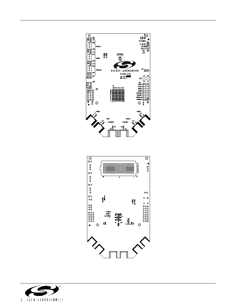
Si5100/Si5110-EVB
Evaluation Board Set for Si5100 and Si5110
OC-48/STM-16 SONET/SDH T
RANSCEIVERS
Description
The Si5100-EVB and Si5110-EVB motherboard/
daughter card sets provide a platform for testing and
characterizing Silicon Laboratories' Si5100/Si5110
SiPHY
TM
OC-48/STM-16 SONET/SDH Transceiver.
The Si5100 and Si5110 transceiver devices provide full-
duplex operation at serial data rates up to 2.7 Gbps.
The transceiver device is mounted on the EVB daughter
card. The high-speed serial signals are accessed via
SMA connectors on the daughter card itself. The low-
speed parallel data channels are routed from the
daughter card to the motherboard through the industry-
standard 300-pin meg-array connector.
The included transceiver loopback motherboard
provides a hardware connection between the
transceiver low-speed parallel data outputs, RXDOUT,
and the transceiver low-speed parallel data inputs,
TXDIN. Test points are provided on the motherboard to
allow monitoring of the parallel data channels. The clock
signals associated with the low-speed data channels
are routed to SMA connectors on the loopback
motherboard. Static control and status signals are
routed to standard 100-mil center posts.
An optional full-duplex motherboard is also available for
the transceiver daughter card. The full-duplex
motherboard also utilizes the industry-standard 300-pin
meg-array connector to allow attachment of the
daughter card. The full-duplex motherboard routes all of
the transceiver low-speed parallel data outputs and
inputs to standard SMA connectors. The optional full-
duplex motherboard is useful when connecting the
transceiver device to a parallel bit error rate tester
(ParBERT), or in other applications that require full
access to the low-speed parallel data channels.
Features
!
Separate supply connections for VDD (1.8 V) and
VDDIO (1.8 V or 3.3 V) allow LVTTL I/Os to be
powered at either 1.8 V or 3.3 V.
!
Control inputs are jumper configurable.
!
Status outputs brought out to headers for easy
access.
!
Potentiometers provided for controlling analog
inputs.
!
Loopback Motherboard (included) provides
hardware path between low-speed parallel data
outputs RXDOUT and low-speed parallel data inputs
TXDIN.
!
Optional full-duplex motherboard provides access to
all low-speed parallel data outputs and inputs via
SMA connectors.
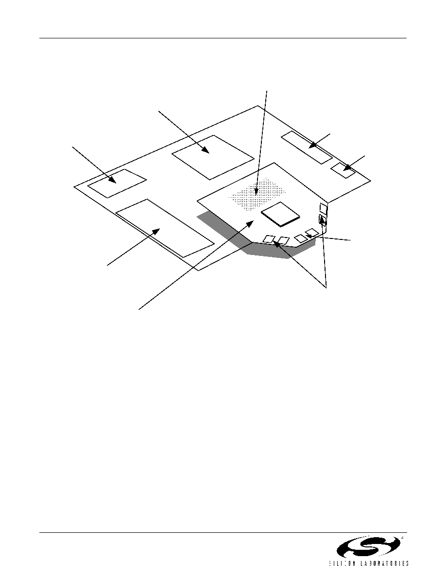
Si5100/Si5110-EVB
2
Preliminary Rev. 0.5
Motherboard/Daughter Card Set
300-Pin Meg-Array Connector
SMA Connectors for Parallel Interface Clock signals
2.5 Gbps Interface SMA Connectors
Daughter Card
Control Input Headers
Status Header
& LEDs
Tra
nsc
eiv
er
Loo
pba
ck
Mo
the
rbo
ard
Si5
100
/
Si5
110
Pow er Connectors
Testpoints
2.5 GHz transmit clock output
Si5100/Si5110-EVB
Preliminary Rev. 0.5
3
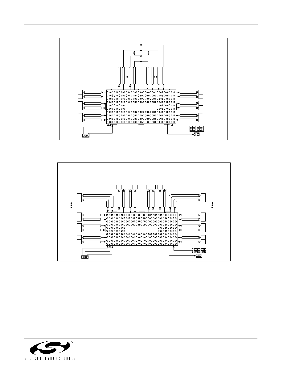
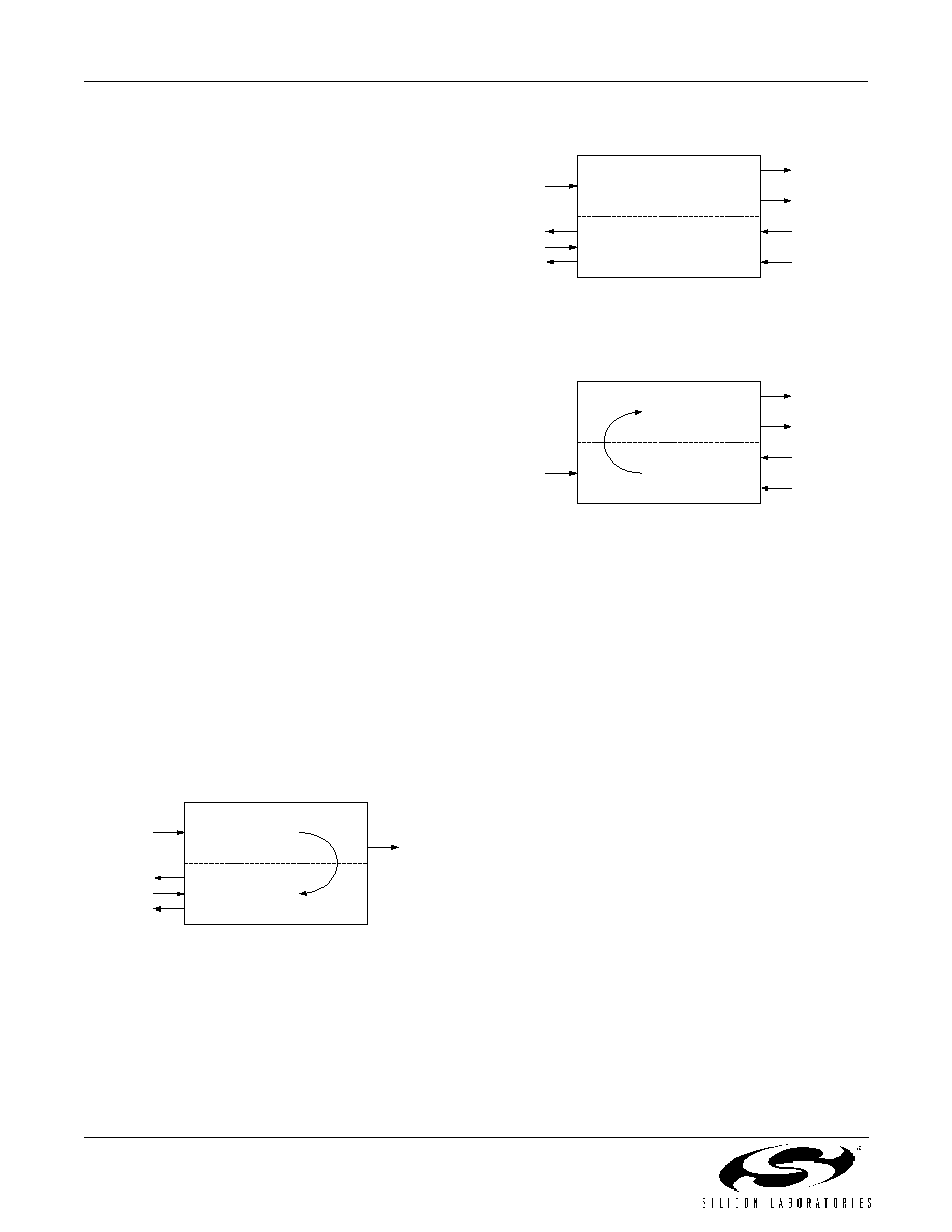
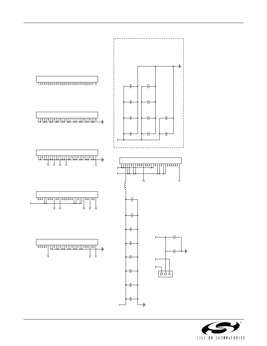
Figure 1. Loopback Motherboard Functional Block Diagram
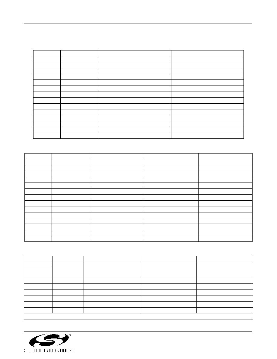
Figure 2. Optional Full-Duplex Motherboard Functional Block Diagram
1.8 V
300-Pin MSA
Connector
GND
Control Inputs
Status Ouputs
3.3 V
TXREFCLK
RXREFCLK
RXCLK1
RXCLK2
TXCLK16IN
TXCLK16OUT
TXDIN Bus
RXDOUT Bus
Testpoints
1.8V
300-Pin MSA
Connector
GND
Control Inputs
Status Ouputs
TXDIN1
RXDOUT0
RXDOUT1
TXDIN15
TX
CLK
1
6
O
UT
TXCLK1
6
I
N
RX
CL
K
1
RX
CL
K
2
RXDOUT15
3.3V
TXDIN0
TXREFCLK
RXREFCLK
Si5100/Si5110-EVB
4
Preliminary Rev. 0.5
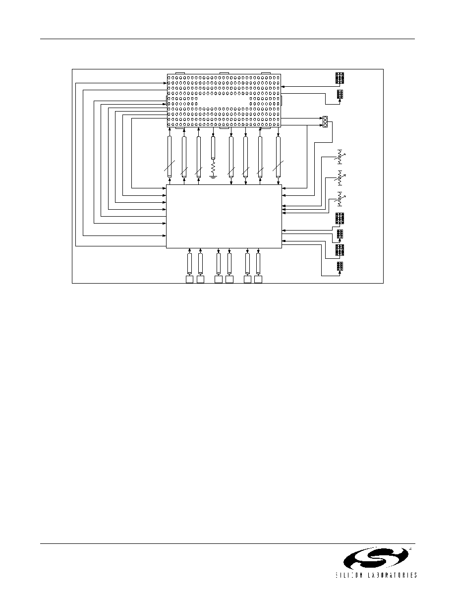
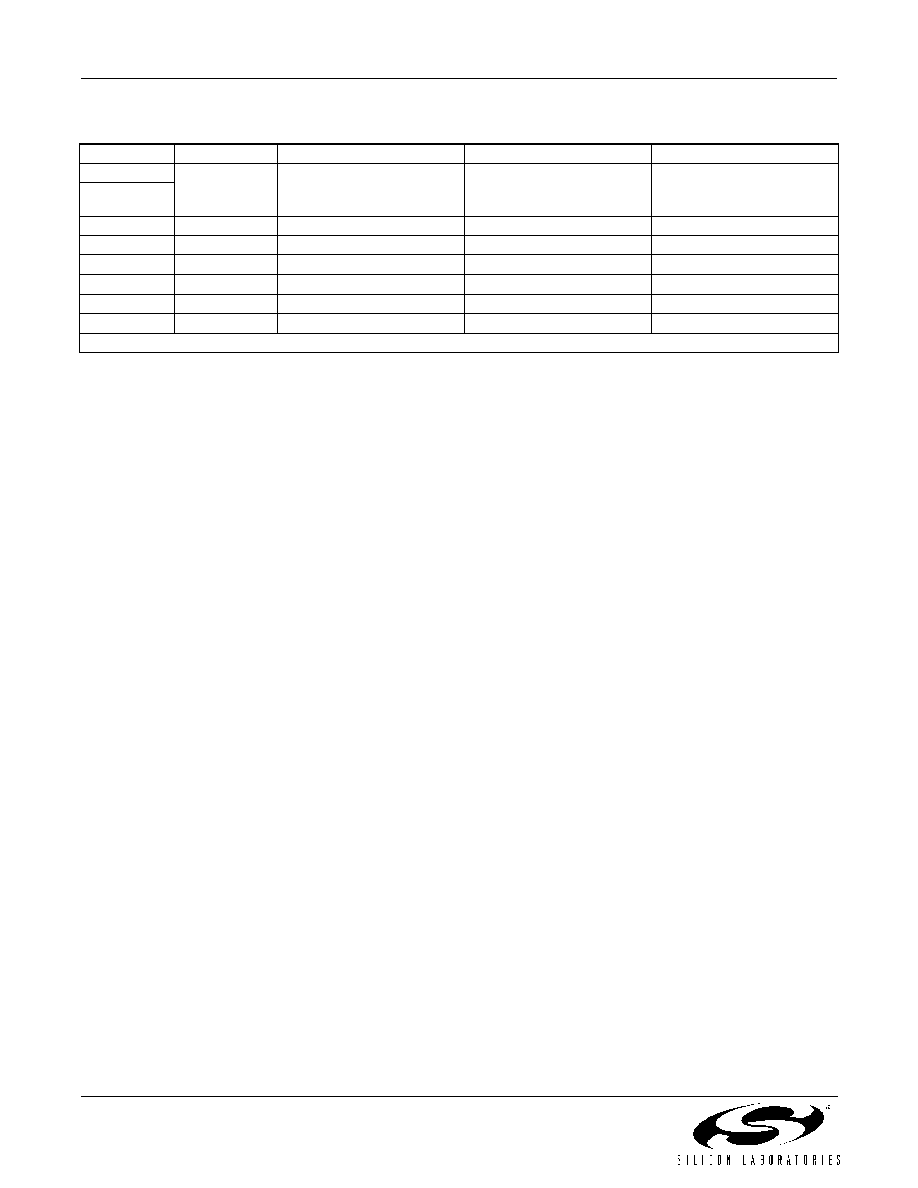
Figure 3. Daughter Card Functional Block Diagram
TXDOUT
TXCLKOUT
RXDIN
Si5100/Si5110
SLICELVL
LOSLVL
PHASEADJ
Test Inputs
TXDIN
16 pairs
RXDOUT
16 pairs
RX
CL
K
1
RX
CL
K
2
RX
RE
F
C
LK
TXR
E
F
C
L
K
TXCL
K1
6
I
N/T
X
CL
K4
IN
TXCL
K1
6
O
UT
/TXCL
K
4OUT
2
2
2
2 2
RESET_N
RXCLK2DSBL_N
RXCLK2DIV_N
FIFOERR_N
FIFORST_N
LPTM_N
Other Input Signals
Other Ouput Signals
Control Inputs
Status Ouputs
Test Ouputs
Control Inputs
Status Ouputs
VDD
VDD33
1.8 V
3.3 V
300-Pin MSA
Connector
VREF
VREF
VREF
Si5100/Si5110-EVB
Preliminary Rev. 0.5
5
Functional Description
The Si5100-EVB and Si5110-EVB motherboard and
daughter card sets simplify characterization of the OC-
48/STM-16 and FEC transceiver devices by providing
convenient access to the device I/Os. Device
performance can be evaluated in various modes by
following the "Basic Test Setup" section.
Power Supply
The transceiver device can be powered from a single
1.8 V supply or seperate 1.8 V and 3.3 V supplies.
When the additional 3.3 V supply is applied, the status
outputs are LVTTL compatible. The daughter card can
be configured for either mode of operation by setting the
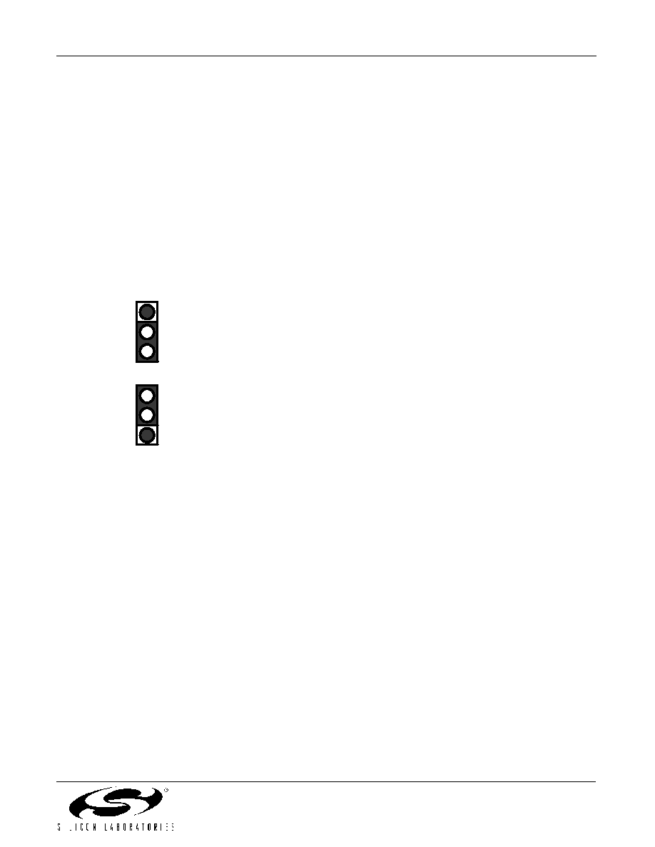
VDD_IO SEL jumper as shown in Figure 4.
Figure 4. VDD_IO Selection Jumpers
Control Inputs
The device control inputs are located on the
motherboard and daughter card. Signals with equivalent
module functions are routed to the motherboard header,
JP1. Signals specific to the transceiver are routed on
the daughter card to jumpers JP1 and JP2. In both
cases, the signal is routed to the center pin of a three
pin group where the adjacent pins are power and
ground. The device inputs are pulled high or low so that
leaving a signal unconnected will not harm the device.
Status Outputs
The device status outputs are located on the
motherboard and daughter card. Signals with equivalent
module functions are routed to the motherboard header,
JP2. Signals specific to the transceiver are routed on
the daughter card to headers JP3 and JP4. In both
cases, the signal is routed to a header pin adjacent to a
ground pin.
Data I/O Signals
The serial 2.5 Gbps data and 2.5 GHz clock paths are
routed as coplanar differentially-coupled microstrip
transmission lines on the daughter card. These three
signals (RXDIN, TXCLKOUT, and TXDOUT) are ac
coupled to standard SMA jacks for ease in connection
to industry standard test equipment. Take care when
connecting cables to these jacks. Use a standard SMA
torque wrench to minimize reflections at the cable-to-
jack interface. Finally, match all differential connections
in length to minimize phase differences between the
positive and negative terminals.
Differential Parallel Data and
Clock I/O Signals
The differential parallel data lines are routed through the
300-pin meg-array connector to the motherboard. The
standard loopback motherboard directly couples the
RXDOUT bus to the TXDIN bus. The optional full-
duplex motherboard directly couples the RXDOUT and
TXDIN buses to standard SMA jacks for connection to
industry standard test equipment.
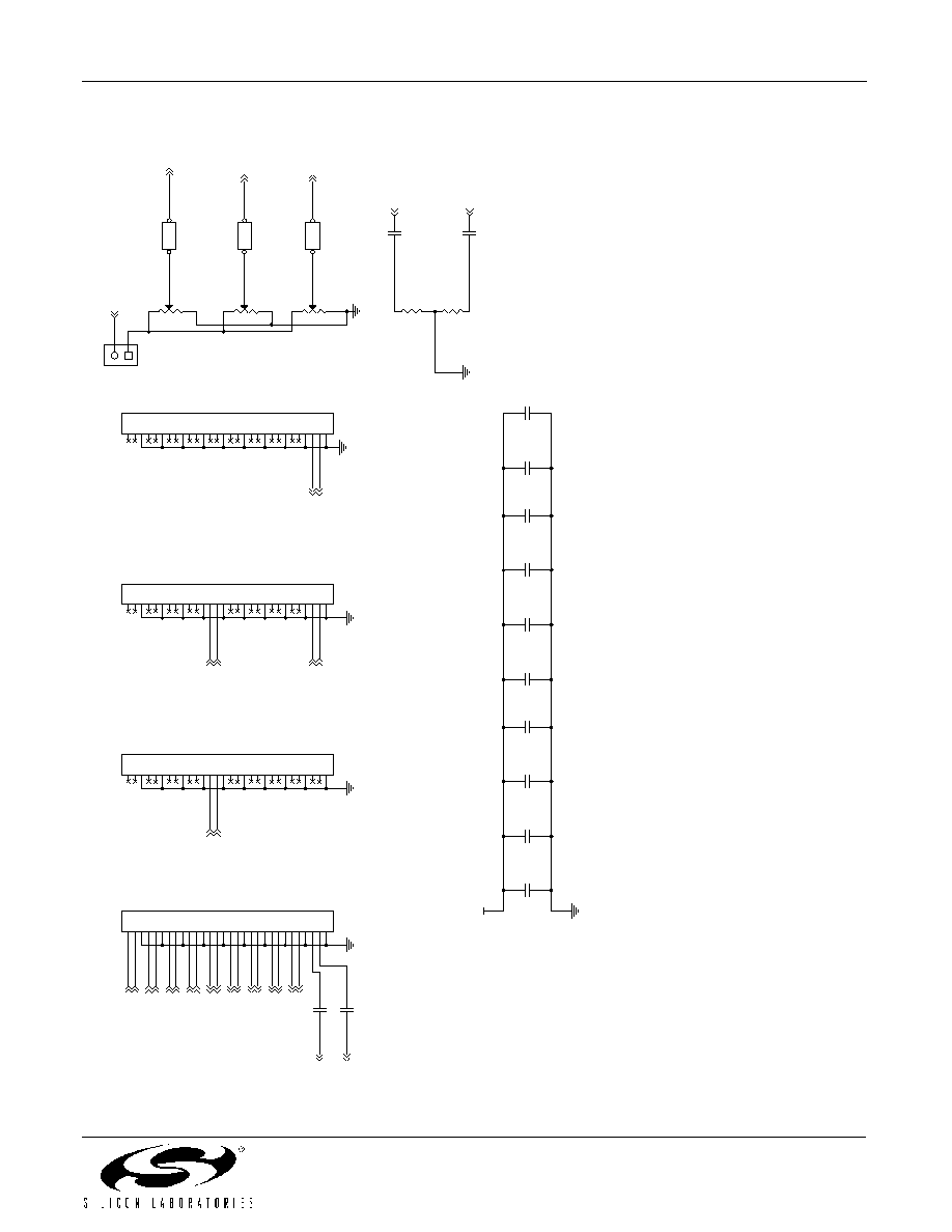
Slice Level, Loss-of-Signal Level, and
Phase Adjust
Voltages present at the Slice Level (SLICELVL), Loss-
of-Signal Level (LOSLVL) and Phase Adjust
(PHASEADJ) pins can be used to adjust the data slicing
level, the loss-of-signal alarm level, and the sampling
phase position, respectively. Because these inputs are
high impedance, simple turn-based potentiometers are
used to apply the control voltage. The Si5100-EVB
provides 50 k
potentiometers for each of these inputs:
potentiometer R16 sets the voltage applied to the
SLICELVL pin; R14 sets the voltage applied to the
LOSLVL pin, and R15 sets the voltage applied to the
PHASEADJ pin. The Si5110-EVB also provides 50 k
potentiometers for each of these inputs. Potentiometer
R5 sets the voltage applied to the SLICELVL pin; R3
sets the voltage applied to the LOSLVL pin, and R4 sets
the voltage applied to the PHASEADJ pin. The
potentiometers are connected so the voltage applied
varies from GND to VREF. Refer to the device data
sheet for details on the operation of these inputs.
Basic Test Setup
The configurations listed in Tables 1 and 3 allow easy
setup of the transceiver evaluation system for operation
in the line loopback, full duplex, or diagnostic loopback
modes. Other configurations are supported; however,
operation should first be verified in one of these modes
in order to minimize the number of unknown variables.
For 1.8 V operation only
VDD_IO
SEL
For 3.3 V/1.8 V operation
VDD_IO
SEL
1.8 V
3.3 V
1.8 V
3.3 V
Si5100/Si5110-EVB
6
Preliminary Rev. 0.5
Line Loopback
When configured in line-loopback mode, the device
passes the received/recovered data and timing to the
transmitter. The transmitter buffers the data through the
FIFO and filters the jitter using the loop-bandwidth
selected by BWSEL[1:0]. Operation in line loopback
mode is depicted in Figure 5. Jumper settings for line
loopback mode are given in Tables 1, 3 (Si5100), and 4
(Si5110). This mode of operation is attainable with both
versions of the motherboard.
Full-Duplex
This mode is identical to normal operation of the device
in a system. TX and RX can be asynchronous (up to
±300 ppm) so all timing is independent. TXCLK16IN is
chosen as the transmitter CMU reference clock via the
REFSEL pin. Operation in full-duplex mode is depicted
in Figure 6. Jumper settings for full-duplex mode are
given in Tables 1, 3 (Si5100), and 4 (Si5110). If the
loopback motherboard is used, the full-duplex mode
effectively becomes an external loopback mode, and
RXCLK1 should be connected to TXCLK16IN/
TXCLK4IN to clock in the data.
Diagnostic Loopback (Parallel Side Loopback)
This mode passes the data present on the transmit
parallel inputs (TXDIN[15:0] for Si5100; TXDIN[3:0] for
Si5110) to the receive parallel data outputs
(RXDOUT[15:0] for Si5100; RXDOUT[3:0] for Si5110).
TXCLK16IN/TXCLK4IN is chosen as the transmitter
CMU reference clock via the REFSEL pin. Operation in
diagnostic loopback mode is depicted in Figure 7.
Jumper settings for diagnostic loopback mode are given
in Tables 2, 3 (Si5100), and 4 (Si5110). The full-duplex
motherboard is required for this mode.
Figure 5. Line Loopback
Figure 6. Full Duplex
Figure 7. Diagnostic Loopback
RXDIN
TXDOUT
TXCLK
RXCLK1
RXDOUT
TXDIN
TXCLK16IN/
TXCLK4IN
Si5100/Si5110
Receiver
Transmitter
TXREFCLK
RXDIN
TXDOUT
TXCLK
RXCLK1
RXDOUT
Si5100/Si5110
Receiver
Transmitter
TXDIN
TXCLK16IN/
TXCLK4IN
TXREFCLK
RXDIN
TXDOUT
TXCLK
RXCLK1
RXDOUT
Si5100/Si5110
Receiver
Transmitter
TXDIN
TXCLK16IN/
TXCLK4IN
TXREFCLK
Si5100/Si5110-EVB
Preliminary Rev. 0.5
7
Both the motherboard and daughter card are placed in line loopback mode before shipment to customers.
Table 1. Loopback Motherboard Setup
Header--Pin
Signal Name
Line Loopback
Asynchronous TX/RX
JP10--2
Voltage Select
3.3 V
3.3 V
JP1--14
RXCLK1DSBL_N
high
high
JP1--11
LTR_N
high
high
JP1--8
RXSQLCH_N
low
high
JP1--5
RXCLK2DIV_N
don't care
don't care
JP1--2
RXCLK2DSBL_N
don't care
don't care
JP2--5
TXREFRATE
high
high
JP2--2
TXRESET_N
high
high
JP3--8
DLBK_N
high
high
JP3--5
LLBK_N
low (enables line loopback)
high
JP3--2
LPTM_N
high
high
JP7--5
RXREFRATE
open
open
JP7--2
RXRESET_N
high
high
JP6--4
FIFORST_N
tie to FIFOERR
tie to FIFOERR
Table 2. Full-Duplex Motherboard Setup
Header--Pin
Signal Name
Line Loopback
Asynchronous TX/RX
Diagnostic Loopback
JP8--2
Voltage Select
3.3 V
3.3 V
3.3 V
JP1--14
RXCLK1DSBL_N
high
high
high
JP1--11
LTR_N
high
high
high
JP1--8
RXSQLCH_N
low
high
high
JP1--5
RXCLK2DIV_N
don't care
don't care
don't care
JP1--2
RXCLK2DSBL_N
don't care
don't care
don't care
JP2--5
REFRATE
high
high
high
JP2--2
RESET_N
high
high
high
JP3--8
DLBK_N
high
high
low
JP3--5
LLBK_N
low (enables line loopback)
high
high
JP3--2
LPTM_N
high
high
high
JP7--5
Si5530 REFRATE
open
open
open
JP7--2
Si5530 RESET_N
high
high
high
JP6--4
FIFORST_N
tie to FIFOERR
tie to FIFOERR
tie to FIFOERR
Table 3. Si5100 Daughter Card Setup
Header--Pin
Signal Name
Line Loopback
Asynchronous TX/RX
Diagnostic Loopback
JP1--20
BWSEL0
BWSEL1
11
(for widest CMU loop
bandwidth)
11
(for widest CMU loop
bandwidth)
11
(for widest CMU loop
bandwidth)
JP1--23
JP1--17
REFSEL
high
high
high
JP1--14
MODE16
high
high
high
JP1--11
TXCLKDSBL
low
low
low
JP1--8
TXMSBSEL
low
low
low
JP1--5
TXSQLCH_N
high
high
high
JP1--2
RXMSBSEL
low
low
low
Note: Jump the VDD_IO selection jumper toward the 3.3 V side.
Si5100/Si5110-EVB
8
Preliminary Rev. 0.5
Table 4. Si5110 Daughter Card Setup
Header--Pin
Signal Name
Line Loopback
Asynchronous TX/RX
Diagnostic Loopback
JP1--20
BWSEL0
BWSEL1
11
(for widest CMU loop
bandwidth)
11
(for widest CMU loop
bandwidth)
11
(for widest CMU loop
bandwidth)
JP1--23
JP1--17
REFSEL
high
high
high
JP1--14
TXCLKDSBL
low
low
low
JP1--11
TXMSBSEL
low
low
low
JP1--8
TXSQLCH_N
high
high
high
JP1--5
SLICEMODE
low
low
low
JP1--2
RXMSBSEL
low
low
low
Note: Jump the VDD_IO selection jumper toward the 3.3 V side.
Si5100/Si5110-EVB
Preliminary Rev. 0.5
9
HEADER 8X3
HEADER 5X3
R
e
served for
Facto
r
y
Testin
g
R
e
served for
Facto
r
y
Testin
g
Do NOT
in
st
a
l
l
NC2
R
X
M
SBSEL
TXM
SBSEL
BWSEL0
TXCLK
D
S
B
L
MODE16
REFSEL
TXSQLCH_
N
RSVD_GND5
RSVD_GND4
RSVD_GND7
RSVD_GND6
GND40
BWSEL1
RSVD_GND3
RSVD_GND2
NC1
BWSEL
0
RSVD_GND4
REFSEL
TXM
SBSEL
BWSEL
1
RSVD_GND5
GND40
RSVD_GND6
RSVD_GND7
RSVD_GND1
TXCLK
D
S
B
L
MODE1
6
TXSQLCH_
N
R
X
M
SBSEL
TXDIN0-
TXDIN1-
TXDIN2-
TXDIN3-
TXDIN4-
TXDIN5-
TXDIN6-
TXDIN7-
TXDIN8-
TXDIN9-
TXDIN10-
TXDIN1
1
+
TXDIN1
2
+
TXDIN1
3
+
TXDIN1
4
+
TXDIN1
5
+
TXDI
N
4
+
TXDIN15-
TXDI
N
8
+
TXDI
N
3
+
TXDI
N
7
+
TXDI
N
2
+
TXDIN14-
TXDI
N
9
+
TXDI
N
6
+
TXDIN13-
TXDI
N
5
+
TXDIN11-
TXDIN1
0
+
TXDI
N
1
+
TXDIN12-
TXDI
N
0
+
VREF
Si5530_REFCLK-
TXCLK16
I
N
+
TXCLK16IN
-
RXDO
U
T
0
+
RXDOUT
0
-
RXDOUT
1
-
RXDO
U
T
1
+
RXDOUT
2
-
RXDO
U
T
2
+
RXDOUT
3
-
RXDO
U
T
3
+
RXDOUT
4
-
RXDO
U
T
4
+
RXDOUT
5
-
RXDO
U
T
5
+
RXDOUT
6
-
RXDO
U
T
6
+
RXDOUT
7
-
RXDO
U
T
7
+
RXDOUT
8
-
RXDO
U
T
8
+
RXDO
U
T
9
+
RXDOUT
9
-
RXDOU
T
1
0
+
RXDOUT
1
0
-
RXDOU
T
1
1
+
RXDOUT
1
1
-
RXDOU
T
1
2
+
RXDOUT
1
2
-
RXDOU
T
1
3
+
RXDOUT
1
3
-
RXDOU
T
1
4
+
RXDOUT
1
4
-
RXDOU
T
1
5
+
RXDOUT
1
5
-
RXCL
K
1
+
RXCLK1-
Si5530_REFCLK+
DLBK_N
FIFORST_N
RXCLK1DSBL_N
SLICELVL
LLBK_N
LTR_N
RESET_N
RXCLK2DSBL_N
LOSLVL
LP
TM
_N
REFRATE
PHASEADJ
RXCLK2DIV_N
RXLOL
_
N
FIFOERR_N
RXCL
K
2
+
RXSQLCH_N
TX
CLK
16OUT-
LOS_N
T
X
L
O
L_N
TXC
LK16OU
T
+
RXCLK2-
VDD
VDD_IO
VDD_IO
VDD_IO
J3
J6
J4
J5
JP4
HEADER 3X2
1
3
5
2
4
6
JP7
HEADER 2X1
12
C6
0402 0.033uF
R17
0 ohm
C5
C4
0402 0.033uF
C3
0402 0.033uF
U1
Si5100
M7
F12
K3
M6
H12
J12
G3
C3
E3
D4
H14
G14
H4
L12
G4
D3
F4
K4
C6
C7
M10
M11
E4
A3
A2
B3
B2
C12
C8
E1
D1
F3
D12
A4
B4
A6
B6
A8
B8
B10
A12
B12
A14
C13
C14
E13
E14
G13
A5
B5
A7
B7
A9
B9
A11
B11
A13
B13
B14
D13
D14
F13
F14
H13
A10
C4
C5
C9
C11
E12
G12
K12
M12
G1
H1
L1
K1
L3
M5
M8
M9
N1
N2
P2
P1
N3
P3
P5
N5
P7
N7
P9
N9
P11
N11
P13
N13
M14
M13
K14
K13
P4
N4
P6
N6
P8
N8
P10
N10
P12
N12
P14
N14
L14
L13
J14
J13
B1
C1
C2
D2
E2
F2
G2
H2
J2
K2
L2
M2
F1
J1
M1
J3
M3
J4
M4
D5
L5
D6
L6
D7
L7
D8
L8
D9
L9
D10
L10
D11
E11
F11
G11
H11
J11
K11
L11
E5
F5
G5
H5
J5
K5
E6
F6
G6
H6
J6
K6
E7
F7
G7
H7
J7
K7
E8
F8
G8
H8
J8
K8
E9
F9
G9
H9
J9
K9
E10
F10
G10
H10
J10
K10
H3
C10
L4
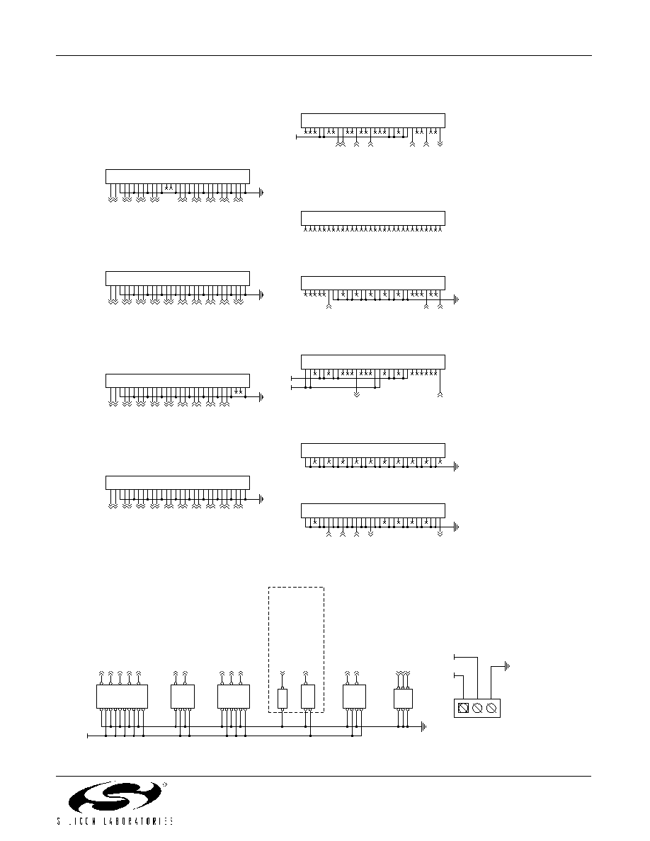
BWSEL[0]
DLBK_N
FIFOERR_N
FIFORST_N
LLBK_N
LPTM_N
LOS_N
LOSLVL
LTR_N
PHASEADJ
REFCLK-
REFCLK+
REFRATE
REFSEL
RESET_N
RSVD_GND3
RXCLK1DSBL_N
RSVD_GND5
RSVD_GND7
RSVD_GND6
BWSEL[1]
RSVD_GND1
GND40
RXCLK1-
RXCLK1+
RXCLK2-
RXCLK2+
RXCLK2DIV_N
RXCLK2DSBL_N
RXDIN-
RXDIN+
RXLOL_N
RXMSBSEL
RXDOUT0+
RXDOUT1+
RXDOUT2+
RXDOUT3+
RXDOUT4+
RXDOUT5+
RXDOUT7+
RXDOUT8+
RXDOUT9+
RXDOUT10+
RXDOUT11+
RXDOUT12+
RXDOUT13+
RXDOUT14+
RXDOUT15+
RXDOUT0-
RXDOUT1-
RXDOUT2-
RXDOUT3-
RXDOUT4-
RXDOUT5-
RXDOUT6-
RXDOUT7-
RXDOUT8-
RXDOUT9-
RXDOUT10-
RXDOUT11-
RXDOUT12-
RXDOUT13-
RXDOUT14-
RXDOUT15-
RXDOUT6+
SLICELVL
VREF
RXSQLCH_N
RXREXT
RSVD_GND2
MODE16
TXCLKDSBL
TXSQLCH_N
TXCLKOUT+
TXCLKOUT-
TXDOUT-
TXDOUT+
TXREXT
TXLOL_N
RSVD_GND4
TXMSBSEL
TXCLK16IN-
TXCLK16IN+
TXCLK16OUT+
TXCLK16OUT-
TXDIN1-
TXDIN0-
TXDIN2-
TXDIN3-
TXDIN4-
TXDIN5-
TXDIN6-
TXDIN7-
TXDIN8-
TXDIN9-
TXDIN10-
TXDIN11-
TXDIN12-
TXDIN13-
TXDIN14-
TXDIN15-
TXDIN0+
TXDIN1+
TXDIN2+
TXDIN3+
TXDIN4+
TXDIN5+
TXDIN6+
TXDIN7+
TXDIN8+
TXDIN9+
TXDIN10+
TXDIN11+
TXDIN12+
TXDIN13+
TXDIN14+
TXDIN15+
GND1
GND2
GND3
GND4
GND5
GND6
GND7
GND8
GND9
GND10
GND11
GND12
GND13
GND14
GND15
GND16
GND17
GND18
GND19
GND20
GND21
GND22
GND23
GND24
GND25
GND26
GND27
GND28
GND29
GND30
GND31
GND32
GND33
GND34
GND35
GND36
GND37
GND38
GND39
VDD1
VDD2
VDD3
VDD4
VDD5
VDD6
VDD7
VDD8
VDD9
VDD10
VDD11
VDD12
VDD13
VDD14
VDD15
VDD16
VDD17
VDD18
VDD19
VDD20
VDD21
VDD22
VDD23
VDD24
VDD25
VDD26
VDD27
VDD28
VDD29
VDD30
VDD31
VDD32
VDD33
VDD34
VDD35
VDD36
VDD_33
NC1
NC2
JP8
HEADER 2X1
12
JP2
2
1
3
45
6
78
9
10
11
12
13
14
15
J2
J1
C1
0402 0.033uF
SW1
SW PUSHBUTTON
C2
0402 0.033uF
R1
0603 3.09k
R2
0603 3.09k
JP1
2
1
3
45
6
78
9
10
11
12
13
14
15
16
17
18
19
20
21
22
24
23
Figure 8
.
Si5100-EVB Daughte
r
Card Sch
e
matic
(p
age 1
of 3)
Si5100/Si5110-EVB
10
Preliminary Rev. 0.5
Place Close to 5100 part on bottom of boa
r
d
LOS_N
RXLOL
_
N
RESET_N
RXCLK2DSBL_N
RXCLK2DIV_N
LP
TM
_N
FIFORST_N
FIFOERR_N
T
X
L
O
L_N
RXCLK1DSBL_N
LLBK_N
REFRATE
LTR_N
RXSQLCH_N
DLBK_N
1.8V
1.8V
3.3V
3.3V
3.3V
VDD
VDD
VDD_IO
C10
0402 100pF
J7F
F1
F2
F3
F4
F5
F6
F7
F8
F9
F10
F11
F12
F13
F14
F15
F16
F17
F18
F19
F20
F21
F22
F23
F24
F25
F26
F27
F28
F29
F30
JP6
+
C13
3216 10 uF
C7
0402 0.1uF
C15
0402 0.1uF
C9
0402 0.1uF
+
C14
3216 10 uF
C11
0402 100pF
J7J
K1
K2
K3
K4
K5
K6
K7
K8
K9
K10
K11
K12
K13
K14
K15
K16
K17
K18
K19
K20
K21
K22
K23
K24
K25
K26
K27
K28
K29
K30
C12
0402 100pF
J7B
B1
B2
B3
B4
B5
B6
B7
B8
B9
B10
B11
B12
B13
B14
B15
B16
B17
B18
B19
B20
B21
B22
B23
B24
B25
B26
B27
B28
B29
B30
C23
0402 100pF
C22
0402 0.1uF
J7H
H1
H2
H3
H4
H5
H6
H7
H8
H9
H10
H11
H12
H13
H14
H15
H16
H17
H18
H19
H20
H21
H22
H23
H24
H25
H26
H27
H28
H29
H30
C21
0402 0.1uF
C24
0402 100pF
J7D
D1
D2
D3
D4
D5
D6
D7
D8
D9
D10
D11
D12
D13
D14
D15
D16
D17
D18
D19
D20
D21
D22
D23
D24
D25
D26
D27
D28
D29
D30
C25
0805 4.7uF
C26
0805 4.7uF
C28
0805 4.7uF
C29
0402 0.1uF
C30
0805 4.7uF
C31
0402 0.1uF
J7I
J1
J2
J3
J4
J5
J6
J7
J8
J9
J10
J11
J12
J13
J14
J15
J16
J17
J18
J19
J20
J21
J22
J23
J24
J25
J26
J27
J28
J29
J30
L1
Murata BLM31P601
S
G
C27
0402 0.1uF
C8
0402 0.1uF
Figure 9
.
Si5100-EVB Daughte
r
Card Sch
e
matic
(p
age 2
of 3)
Si5100/Si5110-EVB
Preliminary Rev. 0.5
11
RXDO
U
T
0
+
RXDO
U
T
1
+
RXDOUT
1
-
RXDOUT
2
-
RXDO
U
T
2
+
RXDO
U
T
3
+
RXDOUT
3
-
RXREFCLK+
RXREFCLK-
RXDOUT
7
-
RXDO
U
T
6
+
RXDOUT
4
-
RXDO
U
T
7
+
RXDO
U
T
5
+
RXDO
U
T
4
+
RXDOUT
5
-
RXDOUT
6
-
R
X
C
LK
2+
RXCLK2
-
RXDOUT
8
-
RXDOUT
1
1
-
RXDO
U
T
9
+
RXDOUT
1
0
-
RXDO
U
T
1
1
+
RXDO
U
T
8
+
RXDOUT
9
-
RXDO
U
T
1
0
+
R
X
C
LK
1+
RXCLK1
-
TX
CLK
16OU
T
+
TX
CLK
16OUT-
RXREFCLK-
RXREFCLK+
LOSLVL
SLICELVL
PHASEADJ
RXDOUT
0
-
RXDO
U
T
1
4
+
RXDO
U
T
1
3
+
RXDOUT
1
2
-
RXDOUT
1
5
-
RXDOUT
1
4
-
RXDO
U
T
1
5
+
RXDOUT
1
3
-
RXDO
U
T
1
2
+
Si5530_REFCLK-
Si5530_REFCLK+
TXDI
N
0
+
TXDIN0-
TXDI
N
1
+
TXDIN1-
TXDI
N
2
+
TXDIN2-
TXDI
N
3
+
TXDIN3-
TXDIN6-
TXDI
N
5
+
TXDI
N
6
+
TXDIN5-
TXDIN7-
TXDI
N
4
+
TXDIN4-
TXDI
N
7
+
TXDIN10-
TXDI
N
9
+
TXDIN1
0
+
TXDIN9-
TXDIN11-
TXDI
N
8
+
TXDIN8-
TXDIN1
1
+
TXDIN1
4
+
TXDIN14-
TXDIN15-
TXDIN1
2
+
TXDIN1
5
+
TXDIN1
3
+
TXDIN13-
TXDIN12-
TXCLK16
I
N
+
TXCLK16IN
-
VREF
R14
PO
T
1
3
2
R15
PO
T
1
3
2
J7A
A1
A2
A3
A4
A5
A6
A7
A8
A9
A10
A11
A12
A13
A14
A15
A16
A17
A18
A19
A20
A21
A22
A23
A24
A25
A26
A27
A28
A29
A30
J7G
G1
G2
G3
G4
G5
G6
G7
G8
G9
G10
G11
G12
G13
G14
G15
G16
G17
G18
G19
G20
G21
G22
G23
G24
G25
G26
G27
G28
G29
G30
JP10
HEADER 2X1
12
C18
0603 0.1uf
C16
0402 0.1uF
C19
0603 0.1uf
JP11
HEADER 2X1
12
C17
0402 0.1uF
J7C
C1
C2
C3
C4
C5
C6
C7
C8
C9
C10
C11
C12
C13
C14
C15
C16
C17
C18
C19
C20
C21
C22
C23
C24
C25
C26
C27
C28
C29
C30
R6
49.9 ohm 1%, 0603
JP12
HEADER 2X1
12
R7
49.9 ohm 1%, 0603
R16
PO
T
1
3
2
J7E
E1
E2
E3
E4
E5
E6
E7
E8
E9
E10
E11
E12
E13
E14
E15
E16
E17
E18
E19
E20
E21
E22
E23
E24
E25
E26
E27
E28
E29
E30
JP9
Figure 10
. Si5100
-EVB Daught
er
Ca
rd
Sc
hematic
(p
age
3 of 3)
Si5100/Si5110-EVB
12
Preliminary Rev. 0.5
Bill of Materials: Si5100-EVB Daughter Card Assembly Revision D-01
Si5100EVB Assy Rev D-01 BOM
Reference
Description
Manu Number
Manufacturer
C1,C2,C3,C4,C5,C6
CAP, SM, 0.033 uF, 0402
C0402X7R160333KNE
VENKEL
C7,C8,C9,C15,C16,C17,
CAP, SM, 0.1 uF, 0402
C0402X7R160104KNE
VENKEL
C21,C22,C27,C29,C31
C10,C11,C12,C23,C24
CAP, SM, 100 pF, 0402
C0402C0G500-101JNE
VENKEL
C14,C13
CAP, SM, 10 uF, TANTALUM, 3216
TA010TCM106KAR
VENKEL
C18,C19
CAP, SM, 0.1 uF, 0603
C0603X7R160-104KNE
VENKEL
C25,C26,C28,C30
CAP,SM,4.7UF,6.3V,X7R,0805
CEJMK212BJ475KG-T
TAIYO YUDEN
JP1
CONNECTOR, HEADER, 8X3
2380-6121TN or 2340-6111TN
3M
JP2
CONNECTOR, HEADER, 5X3
2380-6121TN or 2340-6111TN
3M
JP4
CONNECTOR, HEADER, 3X2
2380-6121TN or 2340-6111TN
3M
JP6
CONNECTOR, HEADER, 3X1
2380-6121TN or 2340-6111TN
3M
JP7,JP8,JP9,JP10,JP11,
CONNECTOR, HEADER, 2X1
2380-6121TN or 2340-6111TN
3M
JP12
J1,J2,J3,J4,J5,J6
CONNECTOR, SMA, NOTCH MOUNT
82 SMA-S50-1-45/111 NE
HUBER SUHNER
J7
CONN,SM,RECPT,MEGARRAY,300 POS BGA
84502-101
FCI/BERG
L1
FERRITE,SM,600 OHM,1500mA
BLM31P601SGPT
MURATA
R1,R2
RESISTOR, SM, 3.09K, 1%, 0603
CR0603-16W-3091FT
VENKEL
R6,R7
RES,SM,49.9,1%,0603
CR0603-16W-49R9FT
VENKEL
R14,R15,R16
POT,50K,10%,MULTITURN TRIMMER
T93YA-50K-10%-D06
VISHAY/DALE
U1
Si5100 Rev D Device
Si5100 Rev D
SILICON LABORATORIES
PCB
Printed Circuit Board
Si5100-EVB Daughter Card PCB Rev D
SILICON LABORATORIES
No Load
SW1
SWITCH, PUSH BUTTON, MINIATURE
101-0161
MOUSER
R17
RES,SM,0,0603
CR0603-16W-000T
VENKEL

Si5100/Si5110-EVB
Preliminary Rev. 0.5
13
RSVD_GND0
RSVD_GND2
RSVD_GND3
RSVD_GND1
RSVD_GND1
TXCLKDSBL
RSVD_GND0
SLICEMODE
TXSQLCH_N
RSVD_GND2
REFSEL
RSVD_GND3
BWSEL0
TX
M
SBSE
L
RXMSBSE
L
BWSEL1
TXCLKDSBL
T
X
M
S
B
SEL
RXMSB
S
E
L
BWSEL0
TXSQLCH_N
REFSEL
BWSEL1
SLICEMODE
TXDIN0-
TXDIN1-
TXDIN3-
TXDIN3+
TXDIN2+
TXDIN1+
TXDIN0+
TXCLK4IN+
TXCLK4IN-
TXCLK
4
O
U
T
+
RXDOUT0+
RXDOUT0-
RXDOUT1-
RXDOUT1+
RXDOUT2-
RXDOUT2+
RXDOUT3-
RXDOUT3+
RXCLK1+
RXCLK1-
RXCLK2DSBL_N
RXSQLCH_N
RXCLK2DIV_N
TXDIN2-
TXCLK4O
U
T
-
RXLOL_N
LOS_N
TXREFCLK+
RESET_N
REFRATE
TXREFCLK-
PHASEADJ
SLICELVL
LOSLVL
RXCLK1DSBL_N
TXLO
L
_
N
RXCLK2-
RXCLK2+
FIFOERR_N
FIFORST_N
VREF
DLBK_N
LTR_N
LPTM_
N
LLBK_N
VDD_IO
VDD_IO
VDD_IO
VDD_IO
VDD
J1
J5
J2
J3
JP4
HEADER 2X1
12
C4
0402 0.1uF
JP2
HEADER 4X3
2
1
3
45
6
78
9
10
12
11
C3
0402 0.1uF
C2
0402 0.1uF
C1
0402 0.1uF
JP1
HEADER 8X3
2
1
3
45
6
78
9
10
11
12
13
14
15
16
17
18
19
20
21
22
23
24
C5
0402 0.1uF
J4
R2
0603 3.09k 1%
JP3
HEADER 2X1
12
JP11
HEADER 1X3
21
3
J6
R1
0603 3.09k 1%
JP10
HEADER 2X1
12
C6
0402 0.1uF
U1
Si5110
H6
H7
J5
H5
H8
G8
D2
B3
C4
A2
F10
E10
F3
J7
E3
C5
D3
J3
A6
B6
H3
G3
B7
A7
A8
C8
C7
C1
B1
C3
D8
A10
A9
C10
C9
B10
B9
D10
D9
A3
B4
A5
A4
C6
J8
J6
E1
F1
J1
H1
K3
K4
J4
H4
K7
K8
K6
K5
K9
K10
H10
H9
J10
J9
G10
G9
E4
F5
F6
G5
G6
G7
G2
B5
K2
B8
B2
C2
D1
E2
E7
E8
E9
F2
F7
F8
F9
G1
H2
J2
K1
E5
E6
F4
G4
D7
D6
D5
D4
BWSEL0
DLBK_N
FIFOERR_N
FIFORST_N
LLBK_N
LPTM_N
LOS_N
LOSLVL
LTR_N
PHASEADJ
REFCLK-
REFCLK+
REFRATE
REFSEL
RESET_N
RSVD_GND4
RXCLK1DSBL_N
RSVD_GND2
RSVD_GND0
RSVD_GND1
BWSEL1
RSVD_GND5
RXCLK1-
RXCLK2-
RXCLK2+
RXCLK2DIV_N
RXCLK2DSBL_N
RXDIN-
RXDIN+
RXLOL_N
RXMSBSEL
RXDOUT0+
RXDOUT1+
RXDOUT2+
RXDOUT3+
RXDOUT0-
RXDOUT1-
RXDOUT2-
RXDOUT3-
SLICELVL
VREF
RXSQLCH_N
RXREXT
SLICEMODE
TXCLKDSBL
TXSQLCH_N
TXCLKOUT+
TXCLKOUT-
TXDOUT-
TXDOUT+
TXREXT
TXLOL_N
RSVD_GND3
TXMSBSEL
TXCLK4IN-
TXCLK4IN+
TXCLK4OUT+
TXCLK4OUT-
TXDIN1-
TXDIN0-
TXDIN2-
TXDIN3-
TXDIN0+
TXDIN1+
TXDIN2+
TXDIN3+
VDD5
VDD9
VDD10
VDD12
VDD13
VDD14
VDD_3
3
RXAMPMON
NC
RXCLK1+
GND1
GND2
GND3
GND4
GND5
GND6
GND7
GND8
GND9
GND10
GND11
GND12
GND13
GND14
GND15
VDD6
VDD7
VDD8
VDD11
VDD4
VDD3
VDD2
VDD1
Figure 1
1
. Si51
10
-EVB Daugh
ter Ca
rd
Sc
hematic
(p
age
1 of 3)
Si5100/Si5110-EVB
14
Preliminary Rev. 0.5
LOS_N
RXLOL
_
N
RESET_N
RXCLK2DSBL_N
RXCLK2DIV_N
FIFORST_N
FIFOERR_N
T
X
L
O
L_N
RXCLK1DSBL_N
REFRATE
LTR_N
RXSQLCH_N
LPT
M
_
N
LLBK_N
DLBK_N
1.8V
1.8V
3.3V
3.3V
VDD
VDD_IO
C14
0402 100pF
J7F
F1
F2
F3
F4
F5
F6
F7
F8
F9
F10
F11
F12
F13
F14
F15
F16
F17
F18
F19
F20
F21
F22
F23
F24
F25
F26
F27
F28
F29
F30
JP5
+
C15
3216 10 uF
C7
0402 0.1uF
+
C16
3216 10 uF
J7J
K1
K2
K3
K4
K5
K6
K7
K8
K9
K10
K11
K12
K13
K14
K15
K16
K17
K18
K19
K20
K21
K22
K23
K24
K25
K26
K27
K28
K29
K30
J7B
B1
B2
B3
B4
B5
B6
B7
B8
B9
B10
B11
B12
B13
B14
B15
B16
B17
B18
B19
B20
B21
B22
B23
B24
B25
B26
B27
B28
B29
B30
J7H
H1
H2
H3
H4
H5
H6
H7
H8
H9
H10
H11
H12
H13
H14
H15
H16
H17
H18
H19
H20
H21
H22
H23
H24
H25
H26
H27
H28
H29
H30
J7D
D1
D2
D3
D4
D5
D6
D7
D8
D9
D10
D11
D12
D13
D14
D15
D16
D17
D18
D19
D20
D21
D22
D23
D24
D25
D26
D27
D28
D29
D30
C10
0805 4.7uF
C12
0402 0.1uF
C9
0805 4.7uF
C11
0402 0.1uF
J7I
J1
J2
J3
J4
J5
J6
J7
J8
J9
J10
J11
J12
J13
J14
J15
J16
J17
J18
J19
J20
J21
J22
J23
J24
J25
J26
J27
J28
J29
J30
L1
Murata BLM31P601S
G
C8
0402 0.1uF
C13
0402 0.1uF
Figure 12
. Si51
10
-EVB Daugh
ter
Ca
rd
Sc
hematic
(p
age
2 of 3)
Si5100/Si5110-EVB
Preliminary Rev. 0.5
15
Place Close to 5110 part on bottom of boa
r
d
RXDO
U
T
0
+
RXDO
U
T
1
+
RXDOUT
1
-
RXDOUT
2
-
RXDO
U
T
2
+
RXDO
U
T
3
+
RXDOUT
3
-
RXCL
K
1
+
RXCLK1-
TXC
LK4O
U
T
+
TXC
LK4OU
T
-
LOSLVL
SLICELVL
PHASEADJ
RXDOUT
0
-
TXREFCLK-
TXREFCL
K
+
TXDI
N
0
+
TXDIN0-
TXDI
N
1
+
TXDIN1-
TXDI
N
2
+
TXDIN2-
TXDI
N
3
+
TXDIN3-
TXCLK4I
N
+
TXCLK4IN-
VREF
RXREFCLK+
RXREFCLK-
RXCLK2-
RXCL
K
2
+
RXREFCLK-
RXREFCLK+
VDD
C19
0603 0.1uf
R3
POT 50K
1
3
2
R4
POT 50K
1
3
2
C21
0402 0.1uF
C22
0402 0.1uF
C25
0402 100pF
C26
0402 100pF
J7A
A1
A2
A3
A4
A5
A6
A7
A8
A9
A10
A11
A12
A13
A14
A15
A16
A17
A18
A19
A20
A21
A22
A23
A24
A25
A26
A27
A28
A29
A30
C27
0402 100pF
C24
0402 0.1uF
J7G
G1
G2
G3
G4
G5
G6
G7
G8
G9
G10
G11
G12
G13
G14
G15
G16
G17
G18
G19
G20
G21
G22
G23
G24
G25
G26
G27
G28
G29
G30
C23
0402 0.1uF
C28
0402 100pF
C29
0805 4.7uF
C30
0805 4.7uF
JP7
HEADER 2X1
12
C17
0603 0.1uF
J7C
C1
C2
C3
C4
C5
C6
C7
C8
C9
C10
C11
C12
C13
C14
C15
C16
C17
C18
C19
C20
C21
C22
C23
C24
C25
C26
C27
C28
C29
C30
JP8
HEADER 2X1
12
C18
0603 0.1uF
R6
49.9 ohm 1%, 0603
JP9
HEADER 2X1
12
R7
49.9 ohm 1%, 0603
R5
POT 50K
1
3
2
J7E
E1
E2
E3
E4
E5
E6
E7
E8
E9
E10
E11
E12
E13
E14
E15
E16
E17
E18
E19
E20
E21
E22
E23
E24
E25
E26
E27
E28
E29
E30
C20
0603 0.1uf
JP6
Figure 13
. Si51
10
-EVB Daugh
ter
Ca
rd
Sc
hematic
(p
age
3 of 3)

Si5100/Si5110-EVB
16
Preliminary Rev. 0.5
Bill of Materials: Si5110-EVB Daughter Card Assembly Revision D-01
Si5110 EVB Daughter Card Assy Rev. E-01 BOM
Reference
Part Desc
Part Number
Manufacturer
C1,C2,C3,C4,C5,C6,C7,C8
CAP,SM,0.1UF,16V,10%,X7R,0402
C0402X7R160-104KNE
VENKEL
C11,C12,C13,C21,C22,C23
C24
C9,C10,C29,C30
CAP,SM,4.7UF,6.3V,X7R,0805
CEJMK212BJ475KG-T
TAIYO YUDEN
C14,C25,C26,C27,C28
CAP,SM,100PF,50V,5%,C0G,0402
C0402C0G500-101JNE
VENKEL
C15,C16
CAP,SM,10UF,10V,10%,TANTALUM,3216
TA010TCM106KAR
VENKEL
C17,C18,C19,C20
CAP,SM,0.1UF,16V,20%,X7R,0603
C0603X7R160-104KNE
VENKEL
JP1
CONN,HEADER,8X3
2380-6121TN or 2340-6111TN
3M
JP5
CONN,HEADER,3X1
2380-6121TN or 2340-6111TN
3M
JP4,JP6,JP7,JP8,JP9
CONN,HEADER,2X1
2380-6121TN or 2340-6111TN
3M
J1,J2,J3,J4,J5,J6
CONNECTOR, SMA, NOTCH MOUNT
82 SMA-S50-1-45/111 NE
HUBER SUHNER
J7
CONN,SM,RECPT,MEGARRAY,300 POS BGA
84502-101
FCI/BERG
L1
FERRITE,SM,600 OHM,1500mA
BLM31P601SGPT
MURATA
R2,R1
RES,SM,3.09K,1%,0603
CR0603-16W-3091FT
VENKEL
R3,R4,R5
POT,50K,10%,MULTITURN TRIMMER
T93YA-50K-10%-D06
VISHAY/DALE
R6,R7
RES,SM,49.9,1%,0603
CR0603-16W-49R9FT
VENKEL
U1
Si5110 Rev E Device
Si5110-BC
SILICON LABS
PCB
Printed Circuit Board
Si5110-EVB Daughter Card PCB Rev C
SILICON LABS
JP2
CONN,HEADER,4X3
2380-6121TN or 2340-6111TN
3M
JP3, JP10
CONN,HEADER,2X1
2380-6121TN or 2340-6111TN
3M
JP11
CONN,HEADER,1X3
2380-6121TN or 2340-6111TN
3M
Si5100/Si5110-EVB
Preliminary Rev. 0.5
17
L
a
y
o
u
t
N
o
t
e
:
A
ll
loopback
data
pai
rs
hav
e t
e
s
t
p
o
in
ts
to
fa
cilita
te
probing access
.
MOTHERBOARD
OUTPUT SIGNAL
VOLTAGE SELECT
3.3V/1.8
V
-
5.
2
V
/
5
V
DATA
8+
DATA
8-
DATA
11-
DATA
13+
DATA
12+
DATA
15+
DATA
12-
DATA
13-
DATA
14-
DATA
15-
DATA
14+
DATA
10-
DATA
9+
DATA
10+
DATA
9-
DATA
11+
RXREFCLK+
RXREFCLK-
TXCLK16IN
-
TXCLK16
I
N
+
TXREFCLK-
TXREFCL
K
+
RXCL
K
2
+
TX
CLK
16OU
T
+
TX
CLK
16OUT-
RXCLK2-
RXCLK1-
RXCL
K
1
+
TXCLK16
I
N
+
TXCLK16IN
-
TX
CLK
16OU
T
+
TX
CLK
16OUT-
RXCL
K
1
+
RXCLK1-
1.8V
3.3V
5V
-5.2V
1.8V
VM
BO
3.3V
R14
0603, 0 ohm
J1E
Meg-Array 300
E1
E2
E3
E4
E5
E6
E7
E8
E9
E10
E11
E12
E13
E14
E15
E16
E17
E18
E19
E20
E21
E22
E23
E24
E25
E26
E27
E28
E29
E30
J4
SM
A
J15
MKDSN 2,5/3-5,08
1
2
3
POS1
POS2
POS3
JP10
R10
0603, 0 ohm
R9
0603, 0 ohm
R7
0603, 0 ohm
R11
0603, 0 ohm
R6
0603, 0 ohm
R12
0603, 0 ohm
R8
0603, 0 ohm
J6
SM
A
J1G
Meg-Array 300
G1
G2
G3
G4
G5
G6
G7
G8
G9
G10
G11
G12
G13
G14
G15
G16
G17
G18
G19
G20
G21
G22
G23
G24
G25
G26
G27
G28
G29
G30
J2
SM
A
J8
SM
A
TP17
1
In
J3
SM
A
R16
0603, 0 ohm
TP19
1
In
J5
SM
A
TP21
1
In
TP18
1
In
J7
SM
A
TP23
1
In
TP20
1
In
J9
SM
A
R5
0603, 0 ohm
TP25
1
In
TP22
1
In
TP27
1
In
TP24
1
In
TP29
1
In
TP26
1
In
J11
SM
A
TP31
1
In
TP28
1
In
J13
SM
A
TP30
1
In
J14
MKDSN 2,5/3-5,08
1
2
3
POS1
POS2
POS3
TP32
1
In
J10
SM
A
R13
0603, 0 ohm
R15
0603, 0 ohm
J12
SM
A
Figure 1
4
. Loopb
ack Motherboard Sche
matic (
p
age 1
of 2)
Si5100/Si5110-EVB
18
Preliminary Rev. 0.5
P
l
a
c
ed together to
al
l
o
w j
u
mperi
ng of
F
I
F
O
E
RR_N to
FIFORST
74244 Decoupling Cap
s
LED ENABLE/
DISABLE
DATA
4-
DATA
5-
DATA
5+
DATA
4+
DATA
6+
DATA
6-
DATA
7+
DATA
7-
DATA
2-
DATA
3+
DATA
0-
DATA
0+
DATA
1+
DATA
3-
DATA
2+
DATA
1-
TXRE
F
R
A
T
E
DLBK_N
LLBK_N
LPT
M
_
N
RXCLK2DSBL_N
FIFORST_N
TXR
ESET_
N
T
X
LOL_N
LOS_N
FIFOERR_N
RXCLK1DSBL_N
TXR
ESET_
N
DLBK_N
LLBK_N
TXRE
F
R
A
T
E
LP
TM
_N
LOS_N
FIFORST_N
RXRESET_
N
RXREFRATE
RXCLK1DSBL_N
RXCLK2DSBL_N
RXCLK2DIV_N
RXSQLCH_N
LTR_N
RXCL
K
2
+
RXCLK2-
LOS_N
T
X
L
O
L_N
RXLOL
_
N
FIFOERR_N
LTR_N
RXLOL
_
N
RXLOL
_
N
RXSQLCH_N
T
X
LOL_N
RXCLK2DIV_N
TXREFCLK-
TXREFCL
K
+
RXREFCLK+
RXREFCLK-
FIFOERR_N
RXRESET_N
RXREFRATE
1.8V
VM
BO
3.3V
-5.2V
5V
3.3V
3.3V
3.3V
TP1
2
1
In
C2
0402 100pF
TP1
4
1
In
TP1
6
1
In
J1F
Meg-Array 300
F1
F2
F3
F4
F5
F6
F7
F8
F9
F10
F11
F12
F13
F14
F15
F16
F17
F18
F19
F20
F21
F22
F23
F24
F25
F26
F27
F28
F29
F30
JP1
HEADER 5X3
2
1
3
45
6
78
9
10
11
12
13
14
15
D3
D4
TP7
1
In
TP9
1
In
J1D
Meg-Array 300
D1
D2
D3
D4
D5
D6
D7
D8
D9
D10
D11
D12
D13
D14
D15
D16
D17
D18
D19
D20
D21
D22
D23
D24
D25
D26
D27
D28
D29
D30
TP11
1
In
J1J
Meg-Array 300
K1
K2
K3
K4
K5
K6
K7
K8
K9
K10
K11
K12
K13
K14
K15
K16
K17
K18
K19
K20
K21
K22
K23
K24
K25
K26
K27
K28
K29
K30
TP13
1
In
J1I
Meg-Array 300
J1
J2
J3
J4
J5
J6
J7
J8
J9
J10
J11
J12
J13
J14
J15
J16
J17
J18
J19
J20
J21
J22
J23
J24
J25
J26
J27
J28
J29
J30
TP15
1
In
R1
365r 0603
TP2
1
In
JP8
HEADER 3X2
1
3
5
2
4
6
R4
365r 0603
R2
365r 0603
JP7
HEADER 2X3
2
1
3
45
6
JP3
1x3 HEADER
1
2
3
12
3
J1H
Meg-Array 300
H1
H2
H3
H4
H5
H6
H7
H8
H9
H10
H11
H12
H13
H14
H15
H16
H17
H18
H19
H20
H21
H22
H23
H24
H25
H26
H27
H28
H29
H30
R3
365r 0603
JP5
HEADER 1X2
12
TP1
1
In
J1A
Meg-Array 300
A1
A2
A3
A4
A5
A6
A7
A8
A9
A10
A11
A12
A13
A14
A15
A16
A17
A18
A19
A20
A21
A22
A23
A24
A25
A26
A27
A28
A29
A30
TP3
1
In
J1B
Meg-Array 300
B1
B2
B3
B4
B5
B6
B7
B8
B9
B10
B11
B12
B13
B14
B15
B16
B17
B18
B19
B20
B21
B22
B23
B24
B25
B26
B27
B28
B29
B30
D1
JP6
HEADER 1X3
2
1
3
TP5
1
In
D2
JP4
HEADER 3X3
2
1
3
45
6
78
9
J1C
Meg-Array 300
C1
C2
C3
C4
C5
C6
C7
C8
C9
C10
C11
C12
C13
C14
C15
C16
C17
C18
C19
C20
C21
C22
C23
C24
C25
C26
C27
C28
C29
C30
C1
0402 0.1uF
TP4
1
In
JP2
HEADER 2X3
2
1
3
45
6
TP6
1
In
TP8
1
In
U1
74LCX244T, 2
0
T
S
S
O
P
1
2
4
6
8
11
13
15
17
19
18
16
14
12
9
7
5
3
20
10
1OE
1A1
1A2
1A3
1A4
2A1
2A2
2A3
2A4
2OE
1Y1
1Y2
1Y3
1Y4
2Y1
2Y2
2Y3
2Y4
VCC
GND
TP1
0
1
In
Figure 1
5
. Loop
back Motherboard Sch
e
matic
(p
age 2
of 2)

Si5100/Si5110-EVB
Preliminary Rev. 0.5
19
Bill of Materials: Loopback Motherboard Assembly Revision A-01
Si5100 Loopback Motherboard Assy Rev A-01
Reference
Part Desc
Part Number
Manufacturer
C1
CAP,SM,0.1UF,16V,10%,X7R,0402
C0402X7R160-104KNE
VENKEL
C2
CAP,SM,100PF,50V,5%,C0G,0402
C0402C0G500-101JNE
VENKEL
D1,D2,D3,D4
LED,SM,RED
LN1271RAL-TR
PANASONIC
JP1
CONN,HEADER,5X3
2380-6121TN or 2340-6111TN
3M
JP2,JP7
CONN,HEADER,2X3
2380-6121TN or 2340-6111TN
3M
JP3,JP6
CONN,HEADER,1X3
2380-6121TN or 2340-6111TN
3M
JP4
CONN,HEADER,3X3
2380-6121TN or 2340-6111TN
3M
JP5
CONN,HEADER,1X2
2380-6121TN or 2340-6111TN
3M
JP8
CONN,HEADER,3X2
2380-6121TN or 2340-6111TN
3M
JP10
CONN,HEADER,3X1
2380-6121TN or 2340-6111TN
3M
J1
CONNECTOR,SM,300 POS,BGA
84500-02
BERG
J2,J3,J4,J5,J6,J7,J8,J9,
CONNECTOR,SMA,SURFACE MOUNT
142-0711-201
JOHNSON COMPONENTS
J10,J11,J12,J13
J15,J14
CONNECTOR,POWER,3 POSITION
1729021
PHOENIX CONTACT
R1,R2,R3,R4
RESISTOR, SM, 365 OHM, 1%, 0603
CR0603-16W-121JT
VENKEL
R5,R6,R7,R8,R9,R10,R11,
RES,SM,0,0402
CR0402-16W-000T
VENKEL
R12,R13,R14,R15,R16
TP1,TP2,TP3,TP4,TP5,TP6,
TEST POINTS ON PCB
N/A
N/A
TP7,TP8,TP9,TP10,TP11,
TP12,TP13,TP14,TP15,TP16,
TP17,TP18,TP19,TP20,TP21,
TP22,TP23,TP24,TP25,TP26,
TP27,TP28,TP29,TP30,TP31,
TP32
U1
IC,SM,74LCX244,20TSSOP
74LCX244MTC
FAIRCHILD
PCB
Printed Circuit Board
Si5100-EVB Loopback Motherboard PCB Rev A
SILICON LABORATORIES
Si5100/Si5110-EVB
20
Preliminary Rev. 0.5
RXDOUT
1
1
-
RXDO
U
T
1
1
+
RXDOUT
1
0
-
RXDO
U
T
1
0
+
RXDOUT
9
-
RXDO
U
T
9
+
RXDOUT
8
-
RXDO
U
T
8
+
RXDOUT
7
-
RXDO
U
T
7
+
RXDOUT
6
-
RXDO
U
T
6
+
RXDO
U
T
1
2
+
RXDOUT
1
2
-
RXDO
U
T
1
3
+
RXDOUT
1
3
-
RXDO
U
T
1
4
+
RXDOUT
1
4
-
RXDO
U
T
1
5
+
RXDOUT
1
5
-
RXCL
K
2
+
RXCLK2-
RXCL
K
1
+
TX
CLK
16OUT-
RXCLK1-
RXDO
U
T
3
+
RXDO
U
T
0
+
RXDOUT
1
-
RXDOUT
4
-
RXDO
U
T
1
+
RXDOUT
2
-
RXDOUT
5
-
RXDO
U
T
2
+
RXDOUT
3
-
RXDOUT
0
-
RXDO
U
T
5
+
RXDO
U
T
4
+
TXC
LK16OU
T
+
TXDI
N
0
+
TXDIN0-
TXDI
N
1
+
TXDIN1-
TXDI
N
2
+
TXDIN2
-
TXDI
N
3
+
TXDIN3
-
TXDI
N
4
+
TXDIN4
-
TXDI
N
5
+
TXDIN5
-
TXDI
N
6
+
TXDIN6
-
TXDI
N
7
+
TXDIN7
-
TXDIN13-
TXDIN1
3
+
TXDIN12-
TXDIN1
2
+
TXDIN11-
TXDIN1
1
+
TXDIN10-
TXDIN1
0
+
TXDIN9-
TXDI
N
9
+
TXDIN8-
TXDI
N
8
+
TXDIN1
4
+
TXDIN14-
TXDIN1
5
+
TXDIN15-
RXREFCLK+
RXREFCLK-
Si5530_REFCLK+
Si5530_REFCLK-
TXCLK16
I
N
+
TXCLK16IN
-
R53
0603, 0 ohm
J26
R36
0603, 0 ohm
R22
0603, 0 ohm
J27
R47
0603, 0 ohm
R11
0603, 0 ohm
J28
R1
0603, 0 ohm
J29
R73
0603, 0 ohm
J30
R54
0603, 0 ohm
J31
R23
0603, 0 ohm
J32
R48
0603, 0 ohm
R27
0603, 0 ohm
R12
0603, 0 ohm
R69
0603, 0 ohm
R37
0603, 0 ohm
J33
R65
0603, 0 ohm
J34
J37
J35
R66
0603, 0 ohm
J38
R55
0603, 0 ohm
J36
J39
R24
0603, 0 ohm
R67
0603, 0 ohm
R28
0603, 0 ohm
J40
R70
0603, 0 ohm
R39
0603, 0 ohm
J41
R68
0603, 0 ohm
J65
SM
A
J42
R3
0603, 0 ohm
J66
SM
A
J43
R56
0603, 0 ohm
J67
SM
A
J44
R74
0603, 0 ohm
R29
0603, 0 ohm
R15
0603, 0 ohm
J68
SM
A
J45
R71
0603, 0 ohm
R40
0603, 0 ohm
J69
SM
A
J46
J70
SM
A
J47
R4
0603, 0 ohm
J71
SM
A
J48
R57
0603, 0 ohm
J72
SM
A
J49
R30
0603, 0 ohm
R16
0603, 0 ohm
J73
SM
A
J50
R72
0603, 0 ohm
R41
0603, 0 ohm
R61
0603, 0 ohm
J74
SM
A
J51
J75
SM
A
J52
R5
0603, 0 ohm
J76
SM
A
J53
R58
0603, 0 ohm
R25
0603, 0 ohm
J1
J54
R31
0603, 0 ohm
R17
0603, 0 ohm
J2
J55
R42
0603, 0 ohm
R6
0603, 0 ohm
R2
0603, 0 ohm
R63
0603, 0 ohm
R13
0603, 0 ohm
J3
J56
R62
0603, 0 ohm
R50
0603, 0 ohm
J4
J57
J5
J58
R59
0603, 0 ohm
R38
0603, 0 ohm
J6
J59
R32
0603, 0 ohm
R18
0603, 0 ohm
J7
J60
R43
0603, 0 ohm
R14
0603, 0 ohm
R7
0603, 0 ohm
R64
0603, 0 ohm
J8
J61
J9
J62
J10
J63
R60
0603, 0 ohm
R49
0603, 0 ohm
J11
J64
R33
0603, 0 ohm
R19
0603, 0 ohm
J12
R44
0603, 0 ohm
R8
0603, 0 ohm
J13
R26
0603, 0 ohm
J14
J15
R51
0603, 0 ohm
J16
R34
0603, 0 ohm
R20
0603, 0 ohm
J17
R45
0603, 0 ohm
R9
0603, 0 ohm
J18
R75
0603, 0 ohm
J19
J20
R52
0603, 0 ohm
J21
R35
0603, 0 ohm
R21
0603, 0 ohm
J22
R46
0603, 0 ohm
R10
0603, 0 ohm
J23
R76
0603, 0 ohm
J24
J25
Figure
16. Full
-
Dup
l
ex Motherboard Sche
matic (p
age 1
of 2)
Si5100/Si5110-EVB
Preliminary Rev. 0.5
21
P
l
a
c
ed together to
al
l
o
w j
u
mperi
ng of
FIFOER
R
t
o
FIFORST
T
X
LOL_N
RXREFCLK+
RXREFCLK-
TXDI
N
0
+
TXDIN0-
TXDI
N
1
+
TXDIN1-
TXDI
N
2
+
TXDIN2-
TXDI
N
3
+
TXDIN3-
Si5530_REFCLK+
Si5530_REFCLK-
TXDI
N
5
+
TXDI
N
6
+
TXDIN6-
TXDIN4-
TXDIN5-
TXDI
N
7
+
TXDIN7-
TXDI
N
4
+
TXDIN11-
TXDIN8-
TXDIN9-
TXDIN1
0
+
TXDI
N
9
+
TXDIN1
1
+
TXDI
N
8
+
TXDIN10-
TXDIN13
-
TXCLK16
I
N
+
TXCLK16IN
-
TXDIN12
-
TXDIN14
-
TXDIN15
-
TXDIN1
4
+
TXDIN1
2
+
TXDIN1
3
+
TXDIN1
5
+
RXSQLCH_N
LTR_N
RXCLK2DIV_N
REFRATE
DLBK_N
LLBK_N
LPT
M
_
N
RXCLK2DSBL_N
FIFORST_N
RESET_N
RXDO
U
T
0
+
RXDOUT
0
-
RXDOUT
1
-
RXDO
U
T
1
+
RXDOUT
2
-
RXDO
U
T
2
+
RXDOUT
3
-
RXDO
U
T
3
+
RXDO
U
T
4
+
RXDOUT
4
-
RXDO
U
T
5
+
RXDOUT
5
-
RXDO
U
T
6
+
RXDOUT
6
-
RXDO
U
T
7
+
RXDOUT
7
-
RXCL
K
2
+
RXCLK2-
RXDO
U
T
8
+
RXDOUT
8
-
RXDO
U
T
9
+
RXDOUT
9
-
RXDO
U
T
1
0
+
RXDOUT
1
0
-
RXDO
U
T
1
1
+
RXDOUT
1
1
-
RXCL
K
1
+
RXCLK1-
TX
CLK
16OU
T
+
TX
CLK
16OUT-
RXDOUT
1
2
-
RXDO
U
T
1
2
+
RXDOUT
1
3
-
RXDO
U
T
1
3
+
RXDOUT
1
4
-
RXDO
U
T
1
4
+
RXDOUT
1
5
-
RXDO
U
T
1
5
+
RXLOL
_
N
T
X
L
O
L_N
LOS_N
FIFOERR_N
RXCLK1DSBL_N
Si5530_REFRATE
Si5530_RESET_N
RESET_N
DLBK_N
LLBK_N
REFRATE
LP
T
M
FIFOERR_N
LOS_N
RXLOL
_
N
FIFORST_N
Si5530_RESET_N
Si5530_REFRATE
RXCLK1DSBL_N
RXCLK2DSBL_N
RXCLK2DIV_N
RXSQLCH_N
LTR_N
1.8V
3.3V
3.3V
3.3V
1.8V
3.3V
J77F
Meg-Array 300
F1
F2
F3
F4
F5
F6
F7
F8
F9
F10
F11
F12
F13
F14
F15
F16
F17
F18
F19
F20
F21
F22
F23
F24
F25
F26
F27
F28
F29
F30
JP1
HEADER 5X3
2
1
3
45
6
78
9
10
11
12
13
14
15
J77E
Meg-Array 300
E1
E2
E3
E4
E5
E6
E7
E8
E9
E10
E11
E12
E13
E14
E15
E16
E17
E18
E19
E20
E21
E22
E23
E24
E25
E26
E27
E28
E29
E30
J77D
Meg-Array 300
D1
D2
D3
D4
D5
D6
D7
D8
D9
D10
D11
D12
D13
D14
D15
D16
D17
D18
D19
D20
D21
D22
D23
D24
D25
D26
D27
D28
D29
D30
J77J
Meg-Array 300
K1
K2
K3
K4
K5
K6
K7
K8
K9
K10
K11
K12
K13
K14
K15
K16
K17
K18
K19
K20
K21
K22
K23
K24
K25
K26
K27
K28
K29
K30
J77I
Meg-Array 300
J1
J2
J3
J4
J5
J6
J7
J8
J9
J10
J11
J12
J13
J14
J15
J16
J17
J18
J19
J20
J21
J22
J23
J24
J25
J26
J27
J28
J29
J30
JP4
HEADER 3X2
1
3
5
2
4
6
J77G
Meg-Array 300
G1
G2
G3
G4
G5
G6
G7
G8
G9
G10
G11
G12
G13
G14
G15
G16
G17
G18
G19
G20
G21
G22
G23
G24
G25
G26
G27
G28
G29
G30
JP7
HEADER 2X3
2
1
3
45
6
J77H
Meg-Array 300
H1
H2
H3
H4
H5
H6
H7
H8
H9
H10
H11
H12
H13
H14
H15
H16
H17
H18
H19
H20
H21
H22
H23
H24
H25
H26
H27
H28
H29
H30
JP5
HEADER 3X2
12
J78
MKDSN 2,5/3-5,08
1
2
3
POS1
POS2
POS3
J77A
Meg-Array 300
A1
A2
A3
A4
A5
A6
A7
A8
A9
A10
A11
A12
A13
A14
A15
A16
A17
A18
A19
A20
A21
A22
A23
A24
A25
A26
A27
A28
A29
A30
J77B
Meg-Array 300
B1
B2
B3
B4
B5
B6
B7
B8
B9
B10
B11
B12
B13
B14
B15
B16
B17
B18
B19
B20
B21
B22
B23
B24
B25
B26
B27
B28
B29
B30
JP6
HEADER 2X3
2
1
3
JP3
HEADER 3X3
2
1
3
45
6
78
9
J77C
Meg-Array 300
C1
C2
C3
C4
C5
C6
C7
C8
C9
C10
C11
C12
C13
C14
C15
C16
C17
C18
C19
C20
C21
C22
C23
C24
C25
C26
C27
C28
C29
C30
JP2
HEADER 2X3
2
1
3
45
6
Figure
17. Full
-
Dup
l
ex Motherboard Sche
matic (p
age 2
of 2)
Si5100/Si5110-EVB
22
Preliminary Rev. 0.5
Bill of Materials: Full-Duplex Motherboard Assembly Revision C-01
Si5100 Motherboard Assy Rev C-01 BOM
Reference
Part Desc
Part Number
Manufacturer
R1,R2,R3,R4,R5,R6,R7,R8,
RES,SM,0,0402
CR0402-16W-000T
VENKEL
R9,R10,R11,R12,R13,R14,
R15,R16,R17,R18,R19,R20,
R21,R22,R23,R24,R25,R26,
R27,R28,R29,R30,R31,R32,
R33,R34,R35,R36,R37,R38,
R39,R40,R41,R42,R43,R44,
R45,R46,R47,R48,R49,R50,
R51,R52,R53,R54,R55,R56,
R57,R58,R59,R60,R61,R62,
R63,R64,R65,R66,R67,R68,
R69,R70,R71,R72,R73,R74,
R75,R76
JP1
CONNECTOR,HEADER,5X3
2340-6111TN or 2380-6121TN
3M
JP2,JP4,JP7
CONNECTOR,HEADER,3X2
2340-6111TN or 2380-6121TN
3M
JP3
CONNECTOR,HEADER,3X3
2340-6111TN or 2380-6121TN
3M
JP5
CONNECTOR,HEADER,2X1
2340-6111TN or 2380-6121TN
3M
JP6
CONNECTOR,HEADER,3X1
2340-6111TN or 2380-6121TN
3M
J1,J2,J3,J4,J5,J6,J7,J8,
CONNECTOR,SMA,SURFACE MOUNT 142-0711-201
JOHNSON COMPONENTS
J9,J10,J11,J12,J13,J14,
J15,J16,J17,J18,J19,J20,
J21,J22,J23,J24,J25,J26,
J27,J28,J29,J30,J31,J32,
J33,J34,J35,J36,J37,J38,
J39,J40,J41,J42,J43,J44,
J45,J46,J47,J48,J49,J50,
J51,J52,J53,J54,J55,J56,
J57,J58,J59,J60,J61,J62,
J63,J64,J65,J66,J67,J68,
J69,J70,J71,J72,J73,J74,
J75,J76
J77
CONNECTOR,SM,300 POS,BGA
84500-02
BERG
J78
CONNECTOR,POWER,3 POSITION
1729021
PHOENIX CONTACT
PCB
Printed Circuit Board
Si5100-EVB Motherboard PCB Rev C
SILICON LABORATORIES
Si5100/Si5110-EVB
Preliminary Rev. 0.5
23
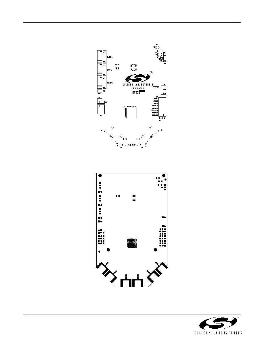
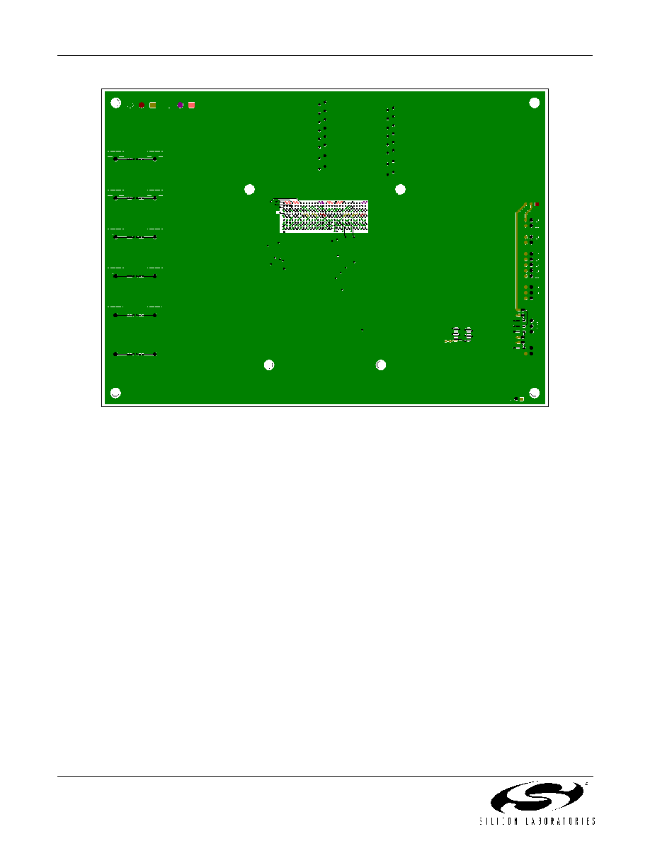
Figure 18. Si5100-EVB Component Side Assembly (Daughter Card)
Figure 19. Si5100-EVB Solder Side Assembly (Daughter Card)
Si5100/Si5110-EVB
24
Preliminary Rev. 0.5
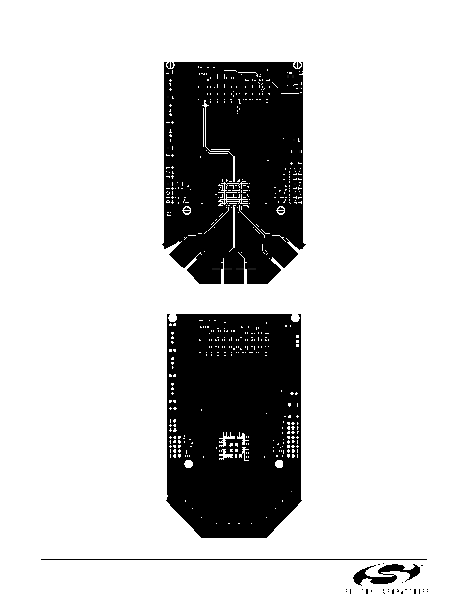
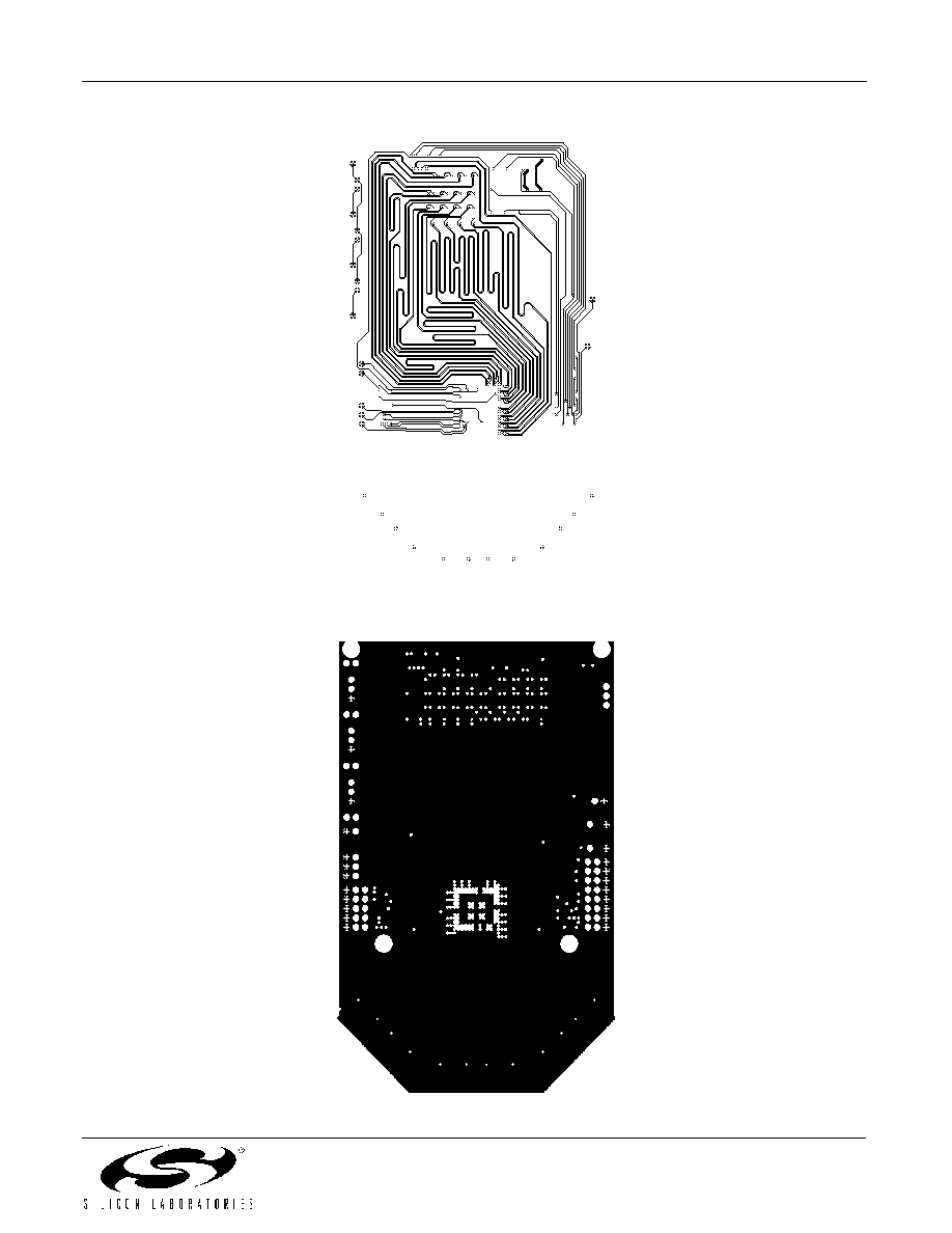
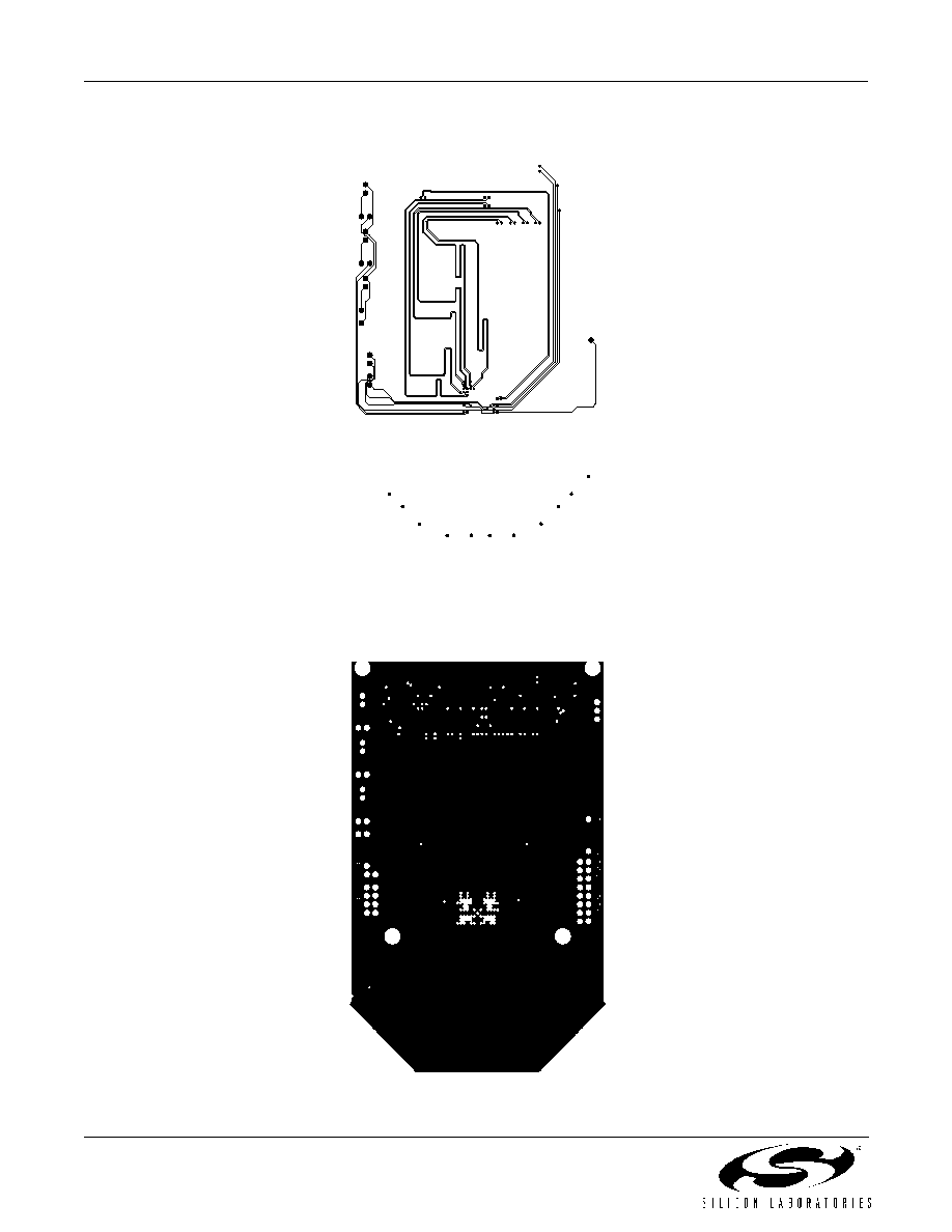
Figure 20. Si5100-EVB Layer 1--Component Side (Daughter Card)
Figure 21. Si5100-EVB Layer 2--GND1 Plane (Daughter Card)
Si5100/Si5110-EVB
Preliminary Rev. 0.5
25
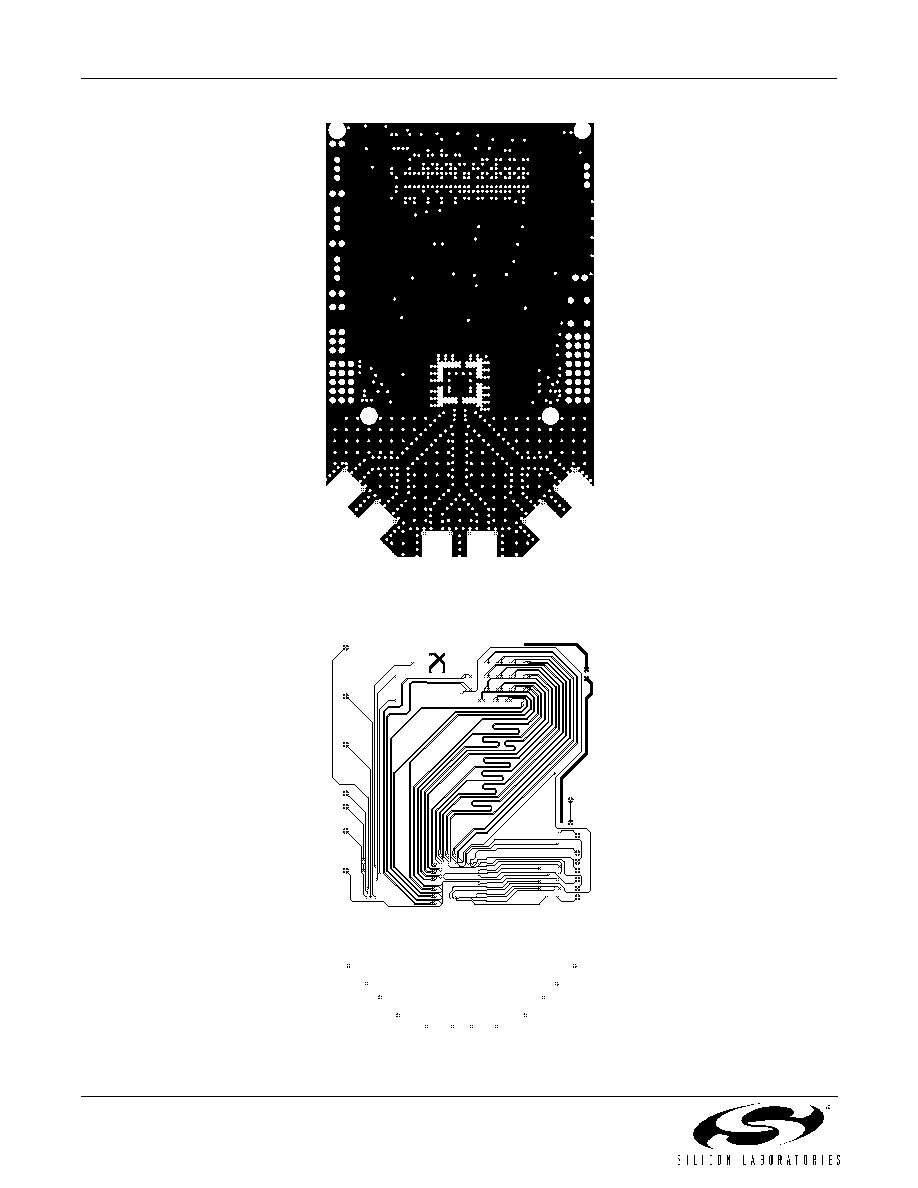
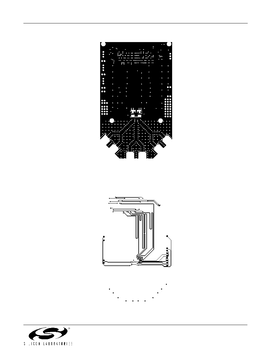
Figure 22. Si5100-EVB Layer 3--Signal Plane (Daughter Card)
Figure 23. Si5100-EVB Layer 4--GND2 Plane (Daughter Card)
Si5100/Si5110-EVB
26
Preliminary Rev. 0.5
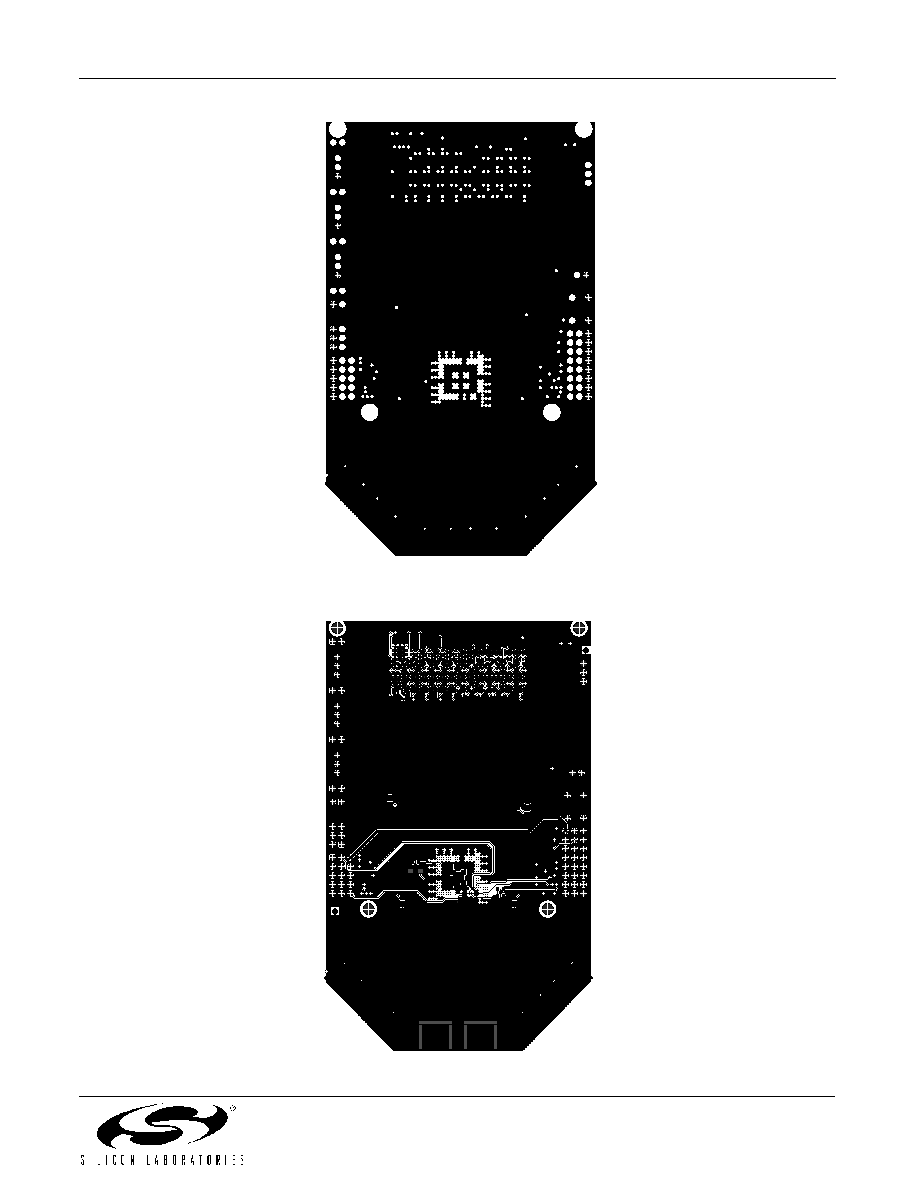
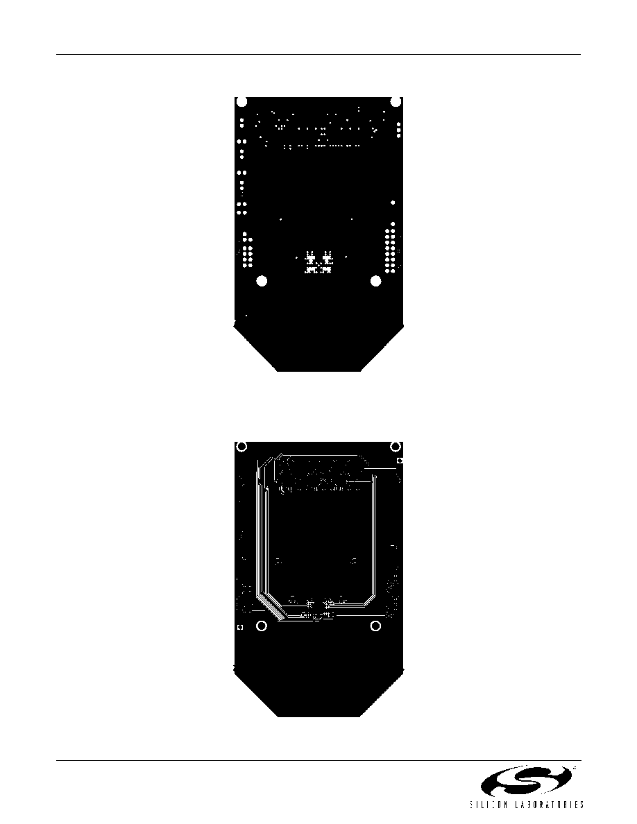
Figure 24. Si5100-EVB Layer 5--VDD Plane (Daughter Card)
Figure 25. Si5100-EVB Layer 6--Signal Plane (Daughter Card)
Si5100/Si5110-EVB
Preliminary Rev. 0.5
27
Figure 26. Si5100-EVB Layer 7--GND3 Plane (Daughter Card)
Figure 27. Si5100-EVB Layer 8--Solder Side (Daughter Card)
Si5100/Si5110-EVB
28
Preliminary Rev. 0.5
Figure 28. Si5110-EVB Component Side Assembly (Daughter Card)
Figure 29. Si5110-EVB Solder Side Assembly (Daughter Card)

Si5100/Si5110-EVB
Preliminary Rev. 0.5
29
Figure 30. Si5110-EVB Layer 1--Component Side (Daughter Card)
Figure 31. Si5110-EVB Layer 2--GND1 Plane (Daughter Card)
Si5100/Si5110-EVB
30
Preliminary Rev. 0.5
Figure 32. Si5110-EVB Layer 3--Signal Plane (Daughter Card)
Figure 33. Si5110-EVB Layer 4--GND2 Plane (Daughter Card)
Si5100/Si5110-EVB
Preliminary Rev. 0.5
31
Figure 34. Si5110-EVB Layer 5--VDD Plane (Daughter Card)
Figure 35. Si5110-EVB Layer 6--Signal Plane (Daughter Card)
Si5100/Si5110-EVB
32
Preliminary Rev. 0.5
Figure 36. Si5110-EVB Layer 7--GND3 Plane (Daughter Card)
Figure 37. Si5110-EVB Layer 8--Solder Side (Daughter Card)
Si5100/Si5110-EVB
Preliminary Rev. 0.5
33
Figure 38. Component Side Assembly (Loopback Motherboard)
Si5100/Si5110-EVB
34
Preliminary Rev. 0.5
Figure 39. Layer 1--Component Side (Loopback Motherboard)
Si5100/Si5110-EVB
Preliminary Rev. 0.5
35
Figure 40. Layer 2--GND1 Plane (Loopback Motherboard)

Si5100/Si5110-EVB
36
Preliminary Rev. 0.5
Figure 41. Layer 3--Signal 1 Plane (Loopback Motherboard)

Si5100/Si5110-EVB
Preliminary Rev. 0.5
37
Figure 42. Layer 4--Signal 2 Plane (Loopback Motherboard)
Si5100/Si5110-EVB
38
Preliminary Rev. 0.5
Figure 43. Layer 5--GND2 Plane (Loopback Motherboard)
Si5100/Si5110-EVB
Preliminary Rev. 0.5
39
Figure 44. Layer 6--Solder Side (Loopback Motherboard)

Si5100/Si5110-EVB
40
Preliminary Rev. 0.5
Figure 45. Component Side Assembly (Optional Full-Duplex Motherboard)
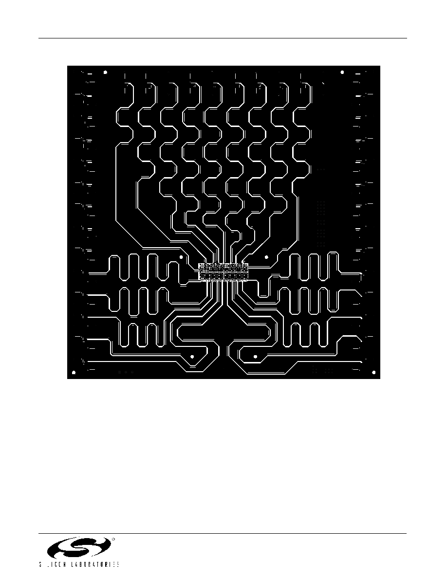
Si5100/Si5110-EVB
Preliminary Rev. 0.5
41
Figure 46. Layer 1--Component Side (Optional Full-Duplex Motherboard)
Si5100/Si5110-EVB
42
Preliminary Rev. 0.5
Figure 47. Layer 2--GND1 Plane (Optional Full-Duplex Motherboard)
Si5100/Si5110-EVB
Preliminary Rev. 0.5
43
Figure 48. Layer 3--Signal 1 Plane (Optional Full-Duplex Motherboard)
Si5100/Si5110-EVB
44
Preliminary Rev. 0.5
Figure 49. Layer 4--Signal 2 Plane (Optional Full-Duplex Motherboard)
Si5100/Si5110-EVB
Preliminary Rev. 0.5
45
Figure 50. Layer 5--GND2 Plane (Optional Full-Duplex Motherboard)
Si5100/Si5110-EVB
46
Preliminary Rev. 0.5
Figure 51. Layer 6--Solder Side (Optional Full-Duplex Motherboard)
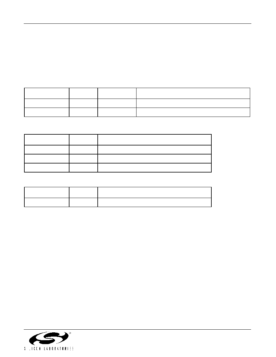
Si5100/Si5110-EVB
Preliminary Rev. 0.5
47
Document Change List
Revision 0.4 to Revision 0.5
!
Split Table 3 into Tables 3 and 4 to reflect differences in the actual PCBs for the Si5100 and Si5110 devices.
!
Updated table references to reflect the changes in Table 3 and the creation of Table 4.
Evaluation Board Assembly Revision History
Si5100-EVB Daughter Card Revision History
Assembly Level
PCB
Si5600 Device
Assembly Notes
C-01
Rev. B
Rev. C
Assemble per BOM rev C-01
D-01
Rev. B
Rev. D
Assemble per BOM rev D-01
Full-Duplex Motherboard Revision History
Assembly Level
PCB
Assembly Notes
A-01
Rev. A
Assemble per BOM rev A-01
B-01
Rev. B
Assemble per BOM rev B-01
C-01
Rev. C
Assemble per BOM rev C-01
Loopback Motherboard Revision History
Assembly Level
PCB
Assembly Notes
A-01
Rev. A
Assemble per BOM rev A-01

Si5100/Si5110-EVB
48
Preliminary Rev. 0.5
Contact Information
Silicon Laboratories Inc.
4635 Boston Lane
Austin, TX 78735
Tel: 1+(512) 416-8500
Fax: 1+(512) 416-9669
Toll Free: 1+(877) 444-3032
Email: productinfo@silabs.com
Internet: www.silabs.com
Silicon Laboratories, Silicon Labs, and DSPLL are trademarks of Silicon Laboratories Inc.
Other products or brandnames mentioned herein are trademarks or registered trademarks of their respective holder
The information in this document is believed to be accurate in all respects at the time of publication but is subject to change without notice.
Silicon Laboratories assumes no responsibility for errors and omissions, and disclaims responsibility for any consequences resulting from
the use of information included herein. Additionally, Silicon Laboratories assumes no responsibility for the functioning of undescribed features
or parameters. Silicon Laboratories reserves the right to make changes without further notice. Silicon Laboratories makes no warranty, rep-
resentation or guarantee regarding the suitability of its products for any particular purpose, nor does Silicon Laboratories assume any liability
arising out of the application or use of any product or circuit, and specifically disclaims any and all liability, including without limitation conse-
quential or incidental damages. Silicon Laboratories products are not designed, intended, or authorized for use in applications intended to
support or sustain life, or for any other application in which the failure of the Silicon Laboratories product could create a situation where per-
sonal injury or death may occur. Should Buyer purchase or use Silicon Laboratories products for any such unintended or unauthorized ap-
plication, Buyer shall indemnify and hold Silicon Laboratories harmless against all claims and damages.