Rev. 2.2 7/04
Copyright © 2004 by Silicon Laboratories
Si5364
Si5364
SONET/SDH P
R E C I S I O N
P
O R T
C
A R D
C
L O C K
IC
Features
Applications
Description
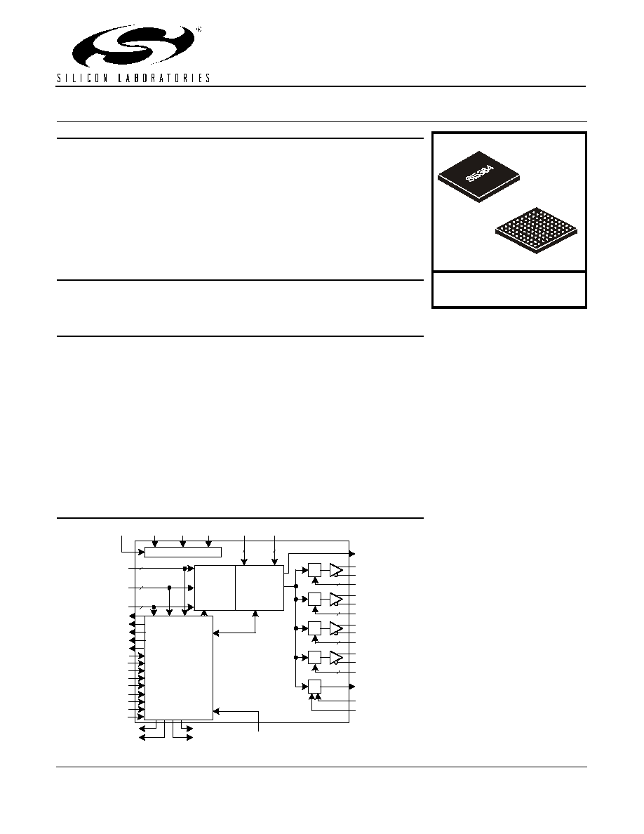
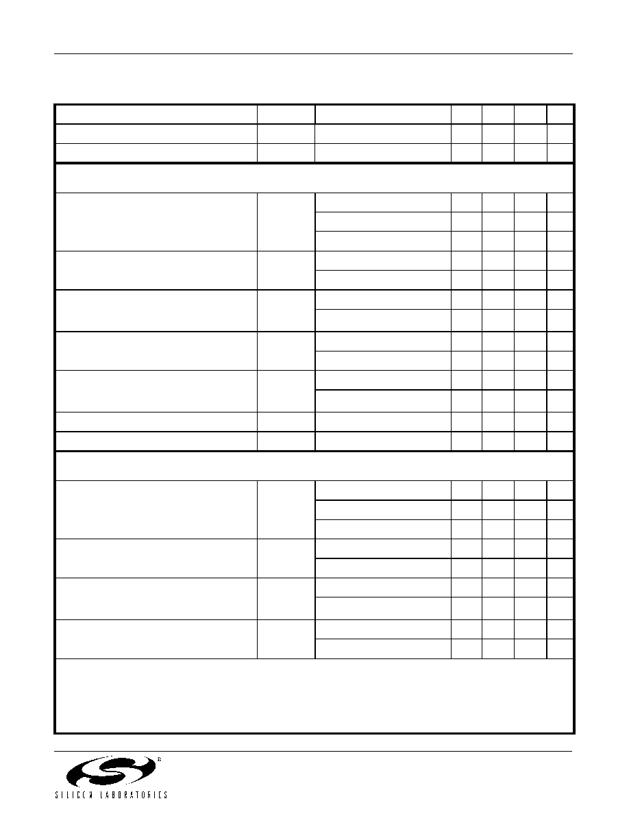
The Si5364 is a complete solution for ultra-low jitter high-speed clock generation and
distribution in precision clocking applications, such as OC-192/OC-48 SONET/SDH line/
port cards. This device phase locks to one of three reference inputs in the range of
19.44 MHz and generates four synchronous clock outputs that can be independently
configured for operation in the 19, 155, or 622 MHz range (1, 8, and 32x input clock).
Silicon Laboratories DSPLLTM technology delivers phase-locked loop (PLL) functionality
with unparalleled performance while eliminating external loop filter components,
providing programmable loop parameters, and simplifying design. The on-chip reference
monitoring and clock switching functions support Stratum 3/3E and SMC compatible
clock switching with excellent output phase transient characteristics. FEC rates are
supported with selectable 255/238 or 238/255 scaling of the clock multiplication ratios.
The Si5364 establishes a new standard in performance and integration for ultra-low jitter
clock generation. It operates from a single 3.3 V supply.
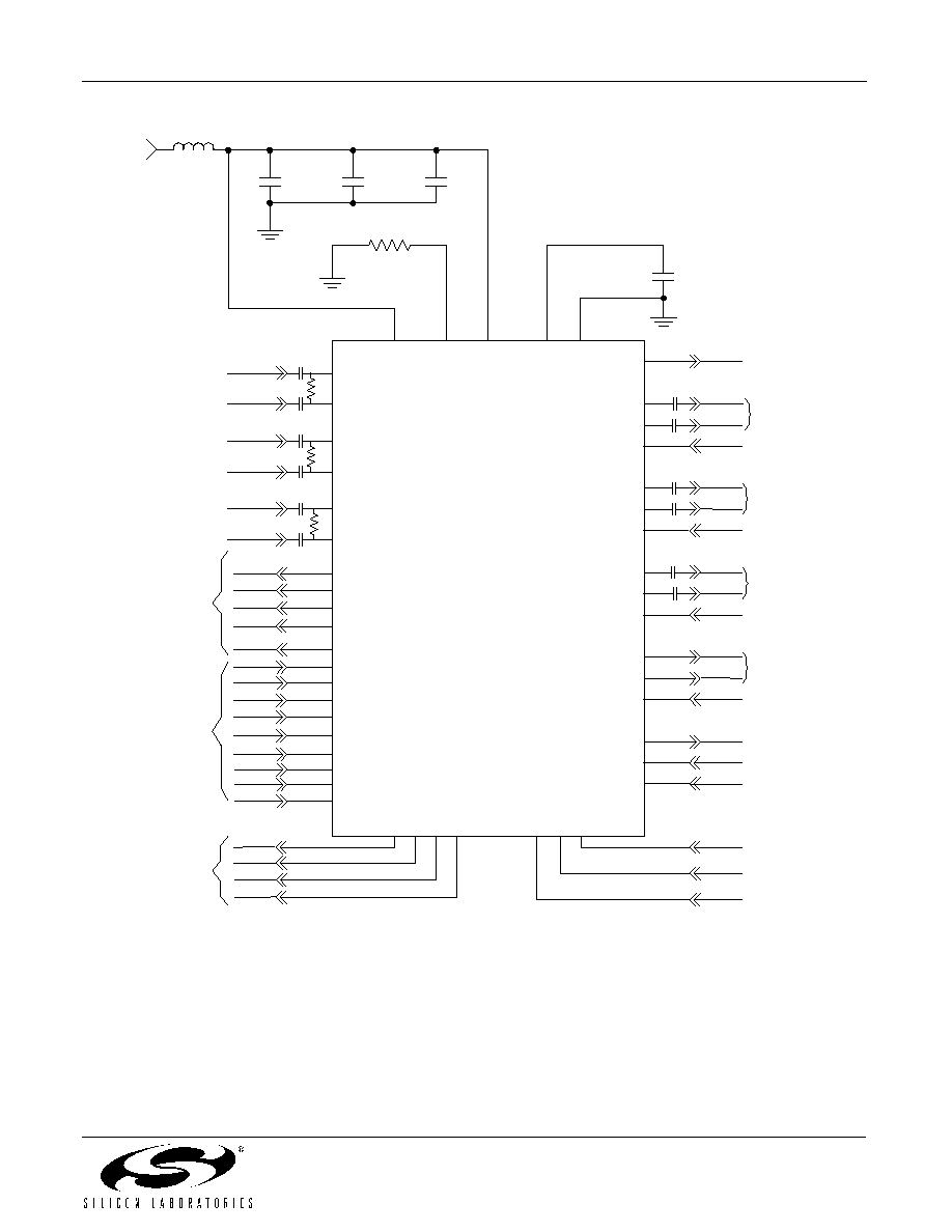
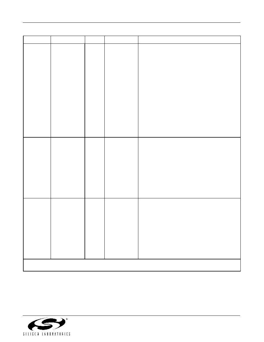
Functional Block Diagram
Ultra-low jitter clock outputs with jitter
generation as low as 0.3 ps
RMS
No external components (other than a
resistor and standard bypassing)
Up to three clock inputs
Four independent clock outputs at 19,
155, or 622 MHz
Stratum 3, 3E, and SMC compatible
Digital hold for loss-of-input clock
Automatic or manually-controlled hitless
switching between clock inputs
Revertive/non-revertive switching
Loss-of-signal and frequency offset
alarms for each clock input
Support for forward and reverse FEC
clock scaling
8 kHz frame sync output
Low power
Small size (11x11 mm)
SONET/SDH line/port cards
Terabit routers
Core switches
Digital cross connects
FRQSEL_1[1:0]
CLKOUT_1+
CLKOUT_1≠
2
2
2
2
DSBLFSYNC
FSYNC
MANCNTRL[1:0]
VALTIME
A_ACTV
LOS_A
FOS_A
LOS_B
FOS_B
LOS_F
REF/CLKIN_F+
REF/CLKIN_F≠
CLKIN_B+
CLKIN_B≠
CLKIN_A+
CLKIN_A≠
AUTOSEL
CAL_ACTV
Signal
Detection,
Selection,
& Control
2
2
2
SMC/S3N
DSBLFOS
RVRT
B_ACTV
F_ACTV
DH_ACTV
RSTN/CAL
FEC[1:0]
BWSEL[1:0]
2
CLKOUT_2+
CLKOUT_2≠
CLKOUT_3+
CLKOUT_3≠
CLKOUT_4+
CLKOUT_4≠
FRQSEL_2[1:0]
FRQSEL_3[1:0]
FRQSEL_4[1:0]
SYNCIN
Biasing & Supply
REXT
VSEL33
VDD
GND
˜
˜
˜
˜
˜
2
SiLECT
TM
Switching
DSPLL
TM
FXDDELAY
INCDELAY
DECDELAY
Ordering Information:
See page 36.
Si5364
Bottom View

Si5364
2
Rev. 2.2

Si5364
Rev. 2.2
3
T
A B L E
O F
C
O N T E N TS
S
E C T I O N
P
AGE
1. Electrical Specifications . . . . . . . . . . . . . . . . . . . . . . . . . . . . . . . . . . . . . . . . . . . . . . . . . . .4
2. Functional Description . . . . . . . . . . . . . . . . . . . . . . . . . . . . . . . . . . . . . . . . . . . . . . . . . . .16
2.1. Clock Output Rate Selection . . . . . . . . . . . . . . . . . . . . . . . . . . . . . . . . . . . . . . . . . . .16
2.2. PLL Performance . . . . . . . . . . . . . . . . . . . . . . . . . . . . . . . . . . . . . . . . . . . . . . . . . . .17
2.3. Frequency Offset and Loss-of-Signal Alarms . . . . . . . . . . . . . . . . . . . . . . . . . . . . . .18
2.4. Loss-of-Signal . . . . . . . . . . . . . . . . . . . . . . . . . . . . . . . . . . . . . . . . . . . . . . . . . . . . . .18
2.5. Input Clock Select Functions . . . . . . . . . . . . . . . . . . . . . . . . . . . . . . . . . . . . . . . . . . .18
2.6. 8 kHz Frame Sync . . . . . . . . . . . . . . . . . . . . . . . . . . . . . . . . . . . . . . . . . . . . . . . . . . .20
2.7. Reset . . . . . . . . . . . . . . . . . . . . . . . . . . . . . . . . . . . . . . . . . . . . . . . . . . . . . . . . . . . . .21
2.8. PLL Self-Calibration . . . . . . . . . . . . . . . . . . . . . . . . . . . . . . . . . . . . . . . . . . . . . . . . .21
2.9. Bias Generation Circuitry . . . . . . . . . . . . . . . . . . . . . . . . . . . . . . . . . . . . . . . . . . . . .21
2.10. Differential Input Circuitry . . . . . . . . . . . . . . . . . . . . . . . . . . . . . . . . . . . . . . . . . . . .21
2.11. Differential Output Circuitry . . . . . . . . . . . . . . . . . . . . . . . . . . . . . . . . . . . . . . . . . . .21
2.12. Power Supply Connections . . . . . . . . . . . . . . . . . . . . . . . . . . . . . . . . . . . . . . . . . . .21
2.13. Design and Layout Guidelines . . . . . . . . . . . . . . . . . . . . . . . . . . . . . . . . . . . . . . . .23
3. Pin Descriptions: Si5364 . . . . . . . . . . . . . . . . . . . . . . . . . . . . . . . . . . . . . . . . . . . . . . . . . .24
4. Ordering Guide . . . . . . . . . . . . . . . . . . . . . . . . . . . . . . . . . . . . . . . . . . . . . . . . . . . . . . . . . .36
5. Package Outline . . . . . . . . . . . . . . . . . . . . . . . . . . . . . . . . . . . . . . . . . . . . . . . . . . . . . . . . .37
6. 11x11 mm CBGA Card Layout . . . . . . . . . . . . . . . . . . . . . . . . . . . . . . . . . . . . . . . . . . . . .38
Document Change List . . . . . . . . . . . . . . . . . . . . . . . . . . . . . . . . . . . . . . . . . . . . . . . . . . . . .39
Contact Information . . . . . . . . . . . . . . . . . . . . . . . . . . . . . . . . . . . . . . . . . . . . . . . . . . . . . . . .40
Si5364
4
Rev. 2.2
1. Electrical Specifications
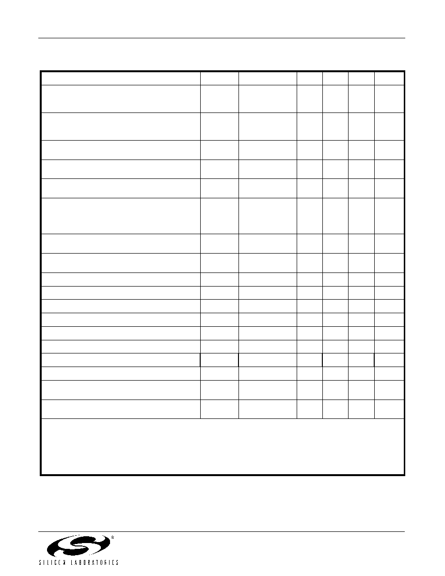
Table 1. Recommended Operating Conditions
1
Parameter
Symbol
Test Condition
Min
1
Typ
Max
1
Unit
Ambient Temperature
T
A
≠20
2
25
85
∞C
Si5364 Supply Voltage
3
When Using 3.3 V Supply
V
DD33
3.135
3.3
3.465
V
Notes:
1. All minimum and maximum specifications are guaranteed and apply across the recommended operating conditions.
Typical values apply at nominal supply voltages and an operating temperature of 25 ∞C unless otherwise stated.
2. The Si5364 is guaranteed by design to operate at ≠40
∞ C.
All electrical specifications are guaranteed for an ambient
temperature of ≠20∞ C to 85∞ C.
3. The Si5364 specifications are guaranteed when using the recommended application circuit (including component
tolerance of Figure 7 on page 15.
Si5364
Rev. 2.2
5
Figure 1. CLKIN Voltage Characteristics
Figure 2. Rise/Fall Time Measurement
*Note: W hen using single-ended clock sources, the unused clock
inputs on the Si5364 must be ac-coupled to ground.
0.5 V
ID
CLKIN+
CLKIN≠
(CLKIN+) ≠ (CLKIN≠)
V
ID
B. Operation with Differential Clock Inputs
V
IS
A. Operation with Single-Ended Clock Inputs*
CLKIN+
CLKIN≠
*Note: Transmission line termination, when required, must be
provided externally.
t
F
t
R
80%
20%
Si5364
6
Rev. 2.2
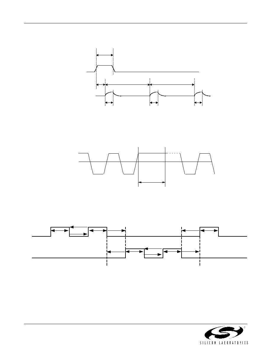
Figure 3. SYNCIN and FSYNC Timing
Figure 4. Transitionless Period on CLKIN for Detecting a LOS Condition
Figure 5.
Clock Input to Clock Output Delay Adjustment
SYNCIN
t
SYNCIN
t
SYNCIN_DLY
FSYNC
1/f
FSYNC
t
FSYNC_PW
1/f
FSYNC
t
FSYNC_PW
t
FSYNC_PW
t
LO S
(C L K IN + ) ≠ (C L K IN ≠ )
0 V
INCDELAY
DECDELAY
t
INCDEC
t
HOLD
t
INCDEC
t
INCDEC
t
HOLD
t
SETUP
t
INCDEC
t
HOLD
t
INCDEC
t
SETUP
t
HOLD
t
SETUP
t
SETUP
Si5364
Rev. 2.2
7
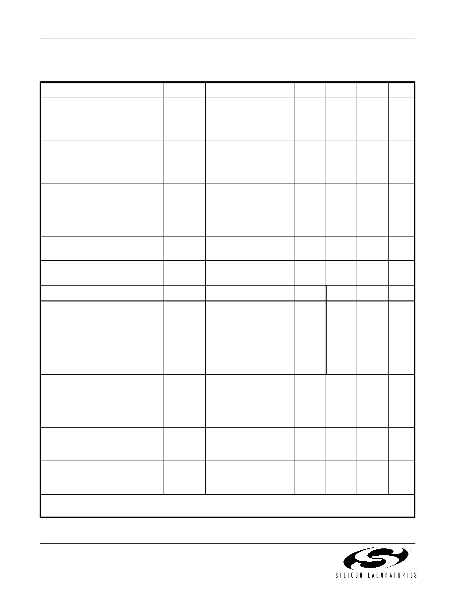
Table 2. DC Characteristics
(V
DD33
= 3.3 V ±5%, T
A
= ≠20 to 85 ∞C)
Parameter
Symbol
Test Condition
Min
Typ
Max
Unit
Supply Current
Single Clock Output
Four Clock Outputs
I
DD
f
out
= 19.44 MHz
--
--
120
212
140
240
mA
Power Dissipation Using 3.3 V Supply
Single Clock Output
Four Clock Outputs
P
D
f
out
= 19.44 MHz
--
396
700
462
792
mW
Common Mode Input Voltage
1,2,3
(CLKIN_A, CLKIN_B, REF/CLKIN_F)
V
ICM
1.0
1.5
2.0
V
Single-Ended Input Voltage
2,3,4
(CLKIN_A, CLKIN_B, REF/CLKIN_F)
V
IS
See Figure 1A
200
--
500
4
mV
PP
Differential Input Voltage Swing
2,3,4
(CLKIN_A, CLKIN_B, REF/CLKIN_F)
V
ID
See Figure 1B
200
--
500
4
mV
PP
Input Impedance
(CLKIN_A+, CLKIN_A-, CLKIN_B+, CLKIN_B≠,
REF/CLKIN_F+,
REF/CLKIN_F≠)
R
IN
--
80
--
k
Differential Output Voltage Swing
(CLKOUT_[3:0])
V
OD
100
Load
Line-to-Line
816
906
1100
mV
PP
Output Common Mode Voltage
(CLKOUT_[3:0])
V
OCM
100
Load
Line-to-Line
1.4
1.8
2.2
V
Output Short to GND (CLKOUT_[3:0])
I
SC(≠)
≠60
--
--
mA
Output Short to V
DD25
(CLKOUT_[3:0])
I
SC(+)
--
≠45
--
mA
Input Voltage Low (LVTTL Inputs)
V
IL
--
--
0.8
V
Input Voltage High (LVTTL Inputs)
V
IH
2.0 --
--
V
Input Low Current (LVTTL Inputs)
I
IL
--
--
50
µA
Input High Current (LVTTL Inputs)
I
IH
--
--
50
µA
Input Impedance (LVTTL Inputs)
R
IN
50
--
--
k
Internal Pulldown (LVTTL inputs)
I
pd
--
--
50
µA
FSYNC Output Charge Current
I
OH_FSYNC
V
FSYNC
= 0 V
C
LOAD
= 10 pF
100
--
--
µA
FSYNC Output Discharge Current
I
OL_FSYNC
V
FSYNC
= V
DD
C
LOAD
= 10 pF
320
--
--
µA
Notes:
1. The Si5364 device provides weak 1.5 V internal biasing that enables ac-coupled operation.
2. Clock inputs may be driven differentially or single-endedly. When driven single-endedly, the unused input should be ac-
coupled to ground.
3. Transmission line termination, when required, must be provided externally.
4. Although the Si5364 device can operate with input clock swings as high as 1500 mV
PP
, Silicon Laboratories recommends
maintaining the input clock amplitude below 500 mV
PP
for optimal performance.
Si5364
8
Rev. 2.2
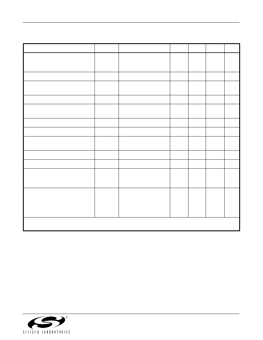
Table 3. AC Characteristics
(V
DD33
= 3.3 V ±5%, T
A
= ≠20 to 85 ∞C)
Parameter
Symbol
Test Condition
Min
Typ
Max
Unit
Input Clock Frequency (non FEC)
*
FEC[1:0] = 00
(CLKIN_A, CLKIN_B, REF/
CLKIN_F)
f
CLKIN
No FEC Scaling
19.436
--
21.093
MHz
Input Clock Frequency (forward
FEC)
*
FEC[1:0] = 01
(CLKIN_A, CLKIN_B, REF/
CLKIN_F)
f
CLKIN
255/238 FEC Scaling
18.140
--
19.687
MHz
Input Clock Frequency (reverse
FEC)
*
FEC[1:0] = 10
(CLKIN_A, CLKIN_B, REF/
CLKIN_F)
f
CLKIN
238/255 FEC Scaling
20.824
--
22.600
MHz
Input Clock Rise Time (CLKIN_A,
CLKIN_B, REF/CLKIN_F)
t
R
Figure 2
--
--
11
ns
Input Clock Fall Time (CLKIN_A,
CLKIN_B, REF/CLKIN_F)
t
F
Figure 2
--
--
11
ns
Input Clock Duty Cycle
C
DUTY_IN
40
50
60
%
Frequency Difference at which
Frequency Offset Alarm (FOS_A,
FOS_B) is declared
(CLKIN_A vs. REF/CLKIN_F,
CLKIN_B vs. REF/CLKIN_F)
SMC/S3N = 1 (SONET Min. Clock)
SMC/S3N = 0 (Stratum 3/3E)
f
FOS
SMC
Stratum3/3E
40
9.2
--
--
72
16.6
±ppm
±ppm
CLKOUT[3:0] Frequency Range
*
FRQSEL[1:0] = 00 (no output)
FRQSEL[1:0] = 01 (1X)
FRQSEL[1:0] = 10 (8X)
FRQSEL[1:0] = 11 (32X)
f
O_19
f
O_155
f
O_622
--
19.436
155.48
621.95
--
--
--
--
--
21.093
168.75
675.0
MHz
MHz
MHz
CLKOUT_[3:0] Rise Time
t
R
Figure 2; single-ended;
after 3 cm of 50
FR4
stripline
--
187
260
ps
CLKOUT_[3:0] Fall Time
t
F
Figure 2; single-ended;
after 3 cm of 50
FR4
stripline
--
176
260
ps
*Note:
The Si5364 provides a 1, 8, or 32x clock frequency multiplication function with an option for additional frequency
scaling by a factor of 255/238 or 238/255 for FEC rate compatibility.
Si5364
Rev. 2.2
9
Output Clock Duty Cycle
C
DUTY_OU
T
Differential:
(CLKOUT+) ≠ (CLKOUT≠
)
48
--
52
%
SYNCIN Pulse Width
t
SYNCIN
Figure 3
20
--
--
ns
FSYNC Frequency
f
FSYNC
Figure 3
--
f
O_19
/
2430
--
kHz
FSYNC Pulse Width
t
FSYNC_PW
Figure 3
--
16
/f
O_19
--
s
SYNCIN to FSYNC
t
SYNCIN_DL
Y
Figure 3
38
45
52
ns
Phase Skew Between Outputs
t
skew
--
--
400
ps
RSTN/CAL Pulse Width
t
RSTN
20
--
--
ns
INCDELAY, DECDELAY Pulse
Width
t
INCDEC
Figure 5
1
--
--
µs
INCDELAY, DECDELAY Setup Time
t
SETUP
Figure 5
1
--
--
µs
INCDELAY, DECDELAY Hold Time
t
HOLD
Figure 5
1
--
--
µs
Transitionless Period Required on
CLKIN for Detecting an LOS Condi-
tion
t
LOS
Figure 4
24/
f
O_622
--
32/
f
O_622
s
Recovery Time for Clearing an LOS
or FOS Condition
VALTIME = 0
VALTIME = 1
t
VAL
Measured from when a
valid reference clock is
applied until the applica-
ble LOS or FOS flag
clears
0.09
12.0
--
--
0.22
14.1
s
Table 3. AC Characteristics (Continued)
(V
DD33
= 3.3 V ±5%, T
A
= ≠20 to 85 ∞C)
Parameter
Symbol
Test Condition
Min
Typ
Max
Unit
*Note:
The Si5364 provides a 1, 8, or 32x clock frequency multiplication function with an option for additional frequency
scaling by a factor of 255/238 or 238/255 for FEC rate compatibility.
Si5364
10
Rev. 2.2
Table 4. AC Characteristics (PLL Performance Characteristics)
(V
DD33
= 3.3 V ± 5%, TA = ≠20 to 85 ∞C)
Parameter
Symbol
Test Condition
Min
Typ
Max Unit
Wander/Jitter at 800 Hz Bandwidth
(BWSEL[1:0] = 10)
Jitter Tolerance (See Figure 8)
J
TOL(PP)
f = 8 Hz
1000
--
--
ns
f = 80 Hz
100
--
--
ns
f = 800 Hz
10
--
--
ns
CLKOUT RMS Jitter Generation
FEC[1:0] = 00 (1/1 Scaling)
J
GEN(RMS)
12 kHz to 20 MHz
--
0.87
1.2
ps
50 kHz to 80 MHz
--
0.26
0.35
ps
CLKOUT RMS Jitter Generation
FEC[1:0] = 01, 10 (255/238, 238/255 Scal-
ing)
J
GEN(RMS)
12 kHz to 20 MHz
--
0.86
1.2
ps
50 kHz to 80 MHz
--
0.26
0.35
ps
CLKOUT Peak-Peak Jitter Generation
FEC[1:0] = 00 (1/1 Scaling)
J
GEN(PP)
12 kHz to 20 MHz
--
6.1
10.0
ps
50 kHz to 80 MHz
--
2.1
5.0
ps
CLKOUT Peak-Peak Jitter Generation
FEC[1:0] = 01, 10 (255/238, 238/255 Scal-
ing)
J
GEN(PP)
12 kHz to 20 MHz
--
6.0
10.0
ps
50 kHz to 80 MHz
--
2.0
5.0
ps
Jitter Transfer Bandwidth (See Figure 9)
F
BW
BW = 800 Hz
--
800
--
Hz
Wander/Jitter Transfer Peaking
J
P
< 800 Hz
--
0.0
0.05
dB
Wander/Jitter at 1600 Hz Bandwidth
(BWSEL[1:0] = 01)
Jitter Tolerance (see Figure 8)
J
TOL(PP)
f = 16 Hz
1000
--
--
ns
f = 160 Hz
100
--
--
ns
f = 1600 Hz
10
--
--
ns
CLKOUT RMS Jitter Generation
FEC[1:0] = 00
J
GEN(RMS)
12 kHz to 20 MHz
--
0.83
1.0
ps
50 kHz to 80 MHz
--
0.26
0.35
ps
CLKOUT RMS Jitter Generation
FEC[1:0] = 01, 10
J
GEN(RMS)
12 kHz to 20 MHz
--
0.8
1.0
ps
50 kHz to 80 MHz
--
0.26
0.35
ps
CLKOUT Peak-Peak Jitter Generation
FEC[1:0] = 00
J
GEN(PP)
12 kHz to 20 MHz
--
5.7
9.0
ps
50 kHz to 80 MHz
--
2.0
5.0
ps
CLKOUT Peak-Peak Jitter Generation
FEC[1:0] = 01, 10
J
GEN(PP)
12 kHz to 20 MHz
--
5.4
9.0
ps
50 kHz to 80 MHz
--
1.9
5.0
ps
Notes:
1.
Higher PLL bandwidth settings provide smaller clock output wander with temperature gradient.
2.
For reliable device operation, temperature gradients should be limited to 10 ∞C/min.
3.
Telcordia GR-1244-CORE requirements specify maximum phase transient slope during clock rearrangement in terms
of nanoseconds per millisecond. The equivalent ps/
µs unit is used here since the maximum phase transient magnitude
for the Si5364 (t
PT_MTIE
) never reaches one nanosecond.
Si5364
Rev. 2.2
11
Jitter Transfer Bandwidth (see Figure 9)
F
BW
BW = 1600 Hz
--
1600
--
Hz
Wander/Jitter Transfer Peaking
J
P
< 1600 Hz
--
0.0
0.1
dB
Wander/Jitter at 3200 Hz Bandwidth
(BWSEL[1:0] = 00)
Jitter Tolerance (see Figure 8)
J
TOL(PP)
f = 32 Hz
1000
--
--
ns
f = 320 Hz
100
--
--
ns
f = 3200 Hz
10
--
--
ns
CLKOUT RMS Jitter Generation
FEC[1:0] = 00 (1/1 Scaling)
J
GEN(RMS)
12 kHz to 20 MHz
--
0.89
1.2
ps
50 kHz to 80 MHz
--
0.3
0.4
ps
CLKOUT RMS Jitter Generation
FEC[1:0] = 01, 10 (255/238, 238/255 Scal-
ing)
J
GEN(RMS)
12 kHz to 20 MHz
--
0.81
1.2
ps
50 kHz to 80 MHz
--
0.30
0.4
ps
CLKOUT Peak-Peak Jitter Generation
FEC[1:0] = 00 (1/1 Scaling)
J
GEN(PP)
12 kHz to 20 MHz
--
5.8
10.0
ps
50 kHz to 80 MHz
--
2.9
5.0
ps
CLKOUT Peak-Peak Jitter Generation
FEC[1:0] = 01, 10 (255/238, 238/255 Scal-
ing)
J
GEN(PP)
12 kHz to 20 MHz
--
7.9
10.0
ps
50 kHz to 80 MHz
--
4.6
5.0
ps
Jitter Transfer Bandwidth (see Figure 9)
F
BW
BW = 3200 Hz
--
3200
--
Hz
Wander/Jitter Transfer Peaking
J
P
< 3200 Hz
--
0.0
0.05
dB
Wander/Jitter at 6400 Hz Bandwidth
(BWSEL[1:0] = 11)
Jitter Tolerance (see Figure 8)
J
TOL(PP)
f = 64 Hz
1000
--
--
ns
f = 640 Hz
100
--
--
ns
f = 6400 Hz
10
--
--
ns
CLKOUT RMS Jitter Generation
FEC[1:0] = 00 (1/1 Scaling)
J
GEN(RMS)
12 kHz to 20 MHz
--
1.03
1.4
ps
50 kHz to 80 MHz
--
0.38
0.5
ps
CLKOUT RMS Jitter Generation
FEC[1:0] = 01, 10 (255/238, 238/255 scal-
ing)
J
GEN(RMS)
12 kHz to 20 MHz
--
1.01
1.4
ps
50 kHz to 80 MHz
--
0.45
0.6
ps
CLKOUT Peak-Peak Jitter Generation
FEC[1:0] = 00 (1/1 Scaling)
J
GEN(PP)
12 kHz to 20 MHz
--
9.3
12.0
ps
50 kHz to 80 MHz
--
2.8
5.5
ps
Table 4. AC Characteristics (PLL Performance Characteristics) (Continued)
(V
DD33
= 3.3 V ± 5%, TA = ≠20 to 85 ∞C)
Parameter
Symbol
Test Condition
Min
Typ
Max Unit
Notes:
1.
Higher PLL bandwidth settings provide smaller clock output wander with temperature gradient.
2.
For reliable device operation, temperature gradients should be limited to 10 ∞C/min.
3.
Telcordia GR-1244-CORE requirements specify maximum phase transient slope during clock rearrangement in terms
of nanoseconds per millisecond. The equivalent ps/
µs unit is used here since the maximum phase transient magnitude
for the Si5364 (t
PT_MTIE
) never reaches one nanosecond.
Si5364
12
Rev. 2.2
CLKOUT Peak-Peak Jitter Generation
FEC[1:0] = 01, 10 (255/238, 238/255 scal-
ing)
J
GEN(PP)
12 kHz to 20 MHz
--
7.1
12.0
ps
50 kHz to 80 MHz
--
3.0
5.5
ps
Jitter Transfer Bandwidth (see Figure 9)
F
BW
BW = 6400 Hz
--
6400
--
Hz
Wander/Jitter Transfer Peaking
J
P
< 6400 Hz
--
0.05
.1
dB
Acquisition Time
T
AQ
RSTN/CAL high to
CAL_ACTV low, with valid
clock input and VALTIME = 0
--
195
350
ms
Clock Output Wander with
Temperature Gradient
1,2
C
CO_TG
Stable Input Clock;
Temperature
Gradient < 10
∞C/min;
800 Hz Loop BW
--
--
40
ps/
∞C/
min
Initial Frequency Accuracy in Digital Hold
Mode (first 100 ms with supply voltage and
temperature held constant)
C
DH_FA
Stable Input Clock
Selected until entering
Digital Hold
--
--
7.0
ppm
Clock Output Frequency Accuracy Over
Temperature in Digital Hold Mode
C
DH_T
Constant Supply Voltage
--
16.2
30
ppm
/
∞C
Clock Output Frequency Accuracy Over
Supply Voltage in Digital Hold Mode
C
DH_V33
Constant Temperature
--
25
500
ppm
/V
Clock Output Phase Step
t
PT_MTIE
During Clock Switching
1/1
≠200
0
200
ps
Clock Output Phase Step Slope
3
--Manual
Switches
BWSEL[1:0] = 11
BWSEL[1:0] = 00
BWSEL[1:0] = 01
BWSEL[1:0] = 10
m
PT
During Clock Switching
6400 Hz
3,200 Hz
1600 Hz
800 Hz
--
--
--
--
--
--
--
--
10
5
2.5
1.25
ps/
µs
Table 4. AC Characteristics (PLL Performance Characteristics) (Continued)
(V
DD33
= 3.3 V ± 5%, TA = ≠20 to 85 ∞C)
Parameter
Symbol
Test Condition
Min
Typ
Max Unit
Notes:
1.
Higher PLL bandwidth settings provide smaller clock output wander with temperature gradient.
2.
For reliable device operation, temperature gradients should be limited to 10 ∞C/min.
3.
Telcordia GR-1244-CORE requirements specify maximum phase transient slope during clock rearrangement in terms
of nanoseconds per millisecond. The equivalent ps/
µs unit is used here since the maximum phase transient magnitude
for the Si5364 (t
PT_MTIE
) never reaches one nanosecond.
Si5364
Rev. 2.2
13
Clock Output Phase Step Slope
3
--Auto
Switching
BWSEL[1:0] = 11
BWSEL[1:0] = 00
BWSEL[1:0] = 01
BWSEL[1:0] = 10
m
PT
During Clock Switching
6400 Hz
3200 Hz
1600 Hz
800 Hz
--
--
--
--
--
--
--
--
36
18
9.0
4.5
ps/
µs
Transient Phase Deviation During Clock
Auto Switching
BWSEL[1:0] = 11
BWSEL[1:0] = 00
BWSEL[1:0] = 01
BWSEL[1:0] = 10
t
pt_mtie_max
6400 Hz
3200 Hz
1600 Hz
800 Hz
--
--
--
--
--
--
--
--
800
800
800
800
ps
Table 5. Absolute Maximum Ratings
Parameter
Symbol
Value
Unit
3.3 V DC Supply Voltage
V
DD33
≠0.5 to 3.6
V
LVTTL Input Voltage
V
DIG
≠0.3 to (+3.6)
V
Maximum Current Any Output PIN
±50
mA
Operating Junction Temperature
T
JCT
≠55 to 150
∞C
Storage Temperature Range
T
STG
≠55 to 150
∞C
ESD HBM Tolerance (100 pf, 1.5 k
)
1.0
kV
Note:
Permanent device damage can occur if the Absolute Maximum Ratings are exceeded. Restrict functional operation to
the conditions as specified in the operational sections of this data sheet. Exposure to absolute maximum rating
conditions for extended periods might affect device reliability.
Table 6. Thermal Characteristics
Parameter
Symbol
Test Condition
Value
Unit
Thermal Resistance Junction to Ambient
JA
Still Air
20
∞C/W
Table 4. AC Characteristics (PLL Performance Characteristics) (Continued)
(V
DD33
= 3.3 V ± 5%, TA = ≠20 to 85 ∞C)
Parameter
Symbol
Test Condition
Min
Typ
Max Unit
Notes:
1.
Higher PLL bandwidth settings provide smaller clock output wander with temperature gradient.
2.
For reliable device operation, temperature gradients should be limited to 10 ∞C/min.
3.
Telcordia GR-1244-CORE requirements specify maximum phase transient slope during clock rearrangement in terms
of nanoseconds per millisecond. The equivalent ps/
µs unit is used here since the maximum phase transient magnitude
for the Si5364 (t
PT_MTIE
) never reaches one nanosecond.
Si5364
14
Rev. 2.2
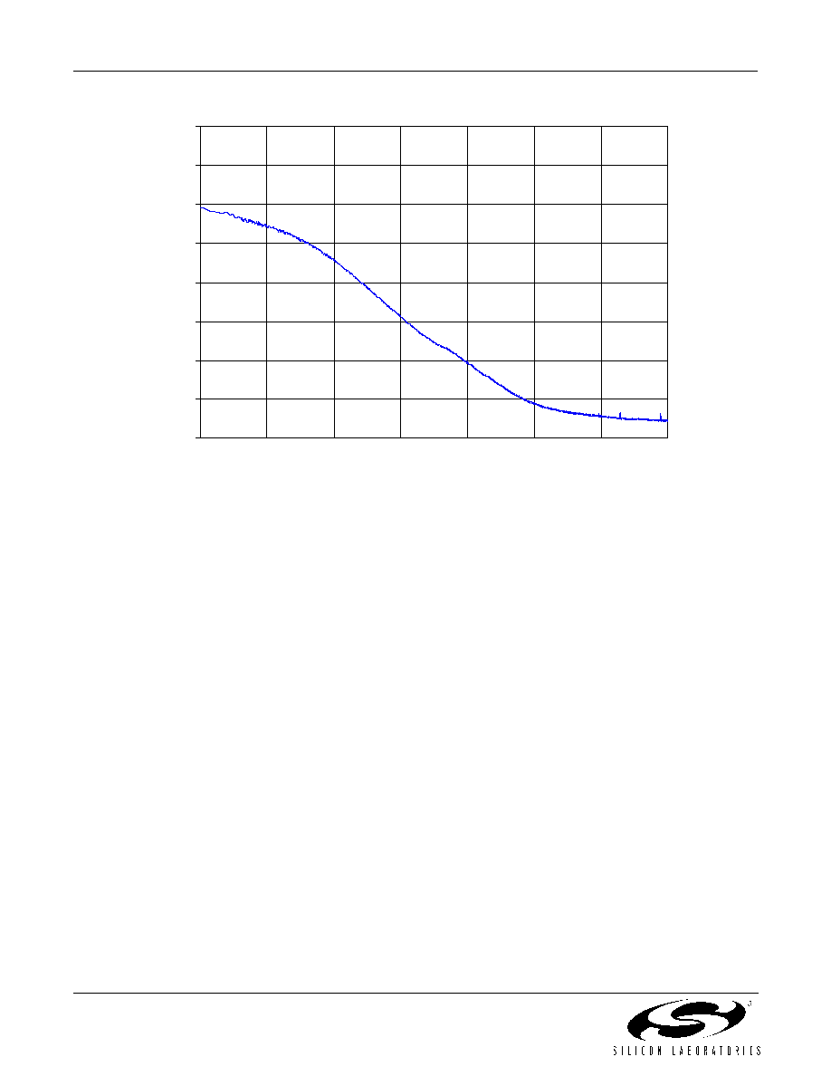
Figure 6. Typical Si5364 Phase Noise (CLKIN = 19.44 MHz, CLKOUT = 622.08 MHz, and
Loop BW = 800 Hz)
10
1
-160
-140
-120
-100
-80
-60
-40
-20
0
10
6
10
5
10
4
10
3
10
2
10
7
10
8
Offset Frequency
Phase Noise (dBc/Hz)
Si5364
Rev. 2.2
15
Figure 7. Si5364 Typical Application Circuit (3.3 V Supply)
10 k
1%
DSBLFOS
LOS_A
FOS_A
LOS_B
FOS_B
LOS_F
REF/CLKIN_F+
CLKIN_A+
SMC/S3N
AUTOSEL
VALTIME
RVRT
CLKIN_A≠
CLKIN_B+
CLKIN_B≠
REF/CLKIN_F≠
19.44 MHz Clock Source 2
19.44 MHz Frequency Reference
19.44 MHz Clock Source 1
Loss of Signal (LOS)
and
Frequency Offset (FOS)
Alarm Signals
Clock Input Selection
and
Control Signals
A_A
C
TV
B_A
C
TV
F_
A
C
TV
DH
_
A
C
T
V
RSTN
/
C
A
L
FEC[
1
:
0
]
BW
SEL
[
1
:
0
]
Reference Clock
Status Indicators
PLL Bandwidth Select
FEC 255/238--238/255
Reset Control
FRQSEL_2[1:0]
CLKOUT_2+
DSBLFSYNC
FSYNC
CAL_ACTV
SYNCIN
CLKOUT_2≠
FRQSEL_4[1:0]
CLKOUT_4+
CLKOUT_4≠
FRQSEL_3[1:0]
CLKOUT_3+
CLKOUT_3≠
FRQSEL_1[1:0]
CLKOUT_1+
CLKOUT_1≠
Clock Output 1
(19, 155, or 622 MHz)
Clock Output 2
(19, 155, or 622 MHz)
Clock Output 1
Frequency Select
Clock Output 2
Frequency Select
Clock Output 3
(19, 155, or 622 MHz)
Clock Output 3
Frequency Select
Clock Output 4
(19, 155, or 622 MHz)
Clock Output 4
Frequency Select
Calibration Active
Status Output
8 kHz FSync Output
Disable FSync Control
FSync Alignment
Sync Pulse Input
RE
XT
V
SEL3
3
VDD
2
5
VDD
3
3
GN
D
0.1
µF
3.3 V Supply
2200 pF
22 pF
33
µF
Si5364
MANCNTRL[1:0]
INCDELAY
DECDELAY
FXDDELAY
Ferrite Bead
0.1
µF
0.1
µF
100
0.1
µF
0.1
µF
100
0.1
µF
0.1
µF
100
0.1
µF
0.1
µF
0.1
µF
0.1
µF
0.1
µF
0.1
µF
Si5364
16
Rev. 2.2
2. Functional Description
The Si5364 is a high-performance precision clock
switching and clock generation device. The Si5364
accepts up to three clock inputs in the 19 MHz range,
selects one of these clocks as the active clock input,
and generates up to four high-quality clock outputs that
are individually-programmable to be 1, 8, or 32x the
input clock frequency. Additional optional scaling by a
factor of 255/238 or 238/255 provides compatibility with
systems that provide or require clocks that are scaled
for forward error correction (FEC) rates. A typical
application for the Si5364 in SONET/SDH systems is
the generation of multiple low-jitter 19.44, 155.52, or
622.08 MHz clock outputs from a single or multiple
(redundant) 19.44 MHz reference clock sources.
The Si5364 employs Silicon Laboratories' DSPLL
technology to provide excellent jitter performance,
minimize the external component count, and maximize
flexibility and ease of use. The Si5364's DSPLL phase
locks to the selected clock input signal, attenuates
significant amounts of jitter, and multiplies the clock
frequency to generate the device's SONET/SDH-
compatible clock outputs. The DSPLL loop bandwidth is
selectable, allowing the Si5364's jitter performance to
be optimized for different applications. The Si5364 can
produce clock outputs with jitter generation as low as
0.30 ps
RMS
(see Table 4 on page 10), making the
device an ideal solution for port card clocking in
SONET/SDH (including OC-48 and OC-192) and
Gigabit Ethernet systems.
Input clock selection and switching occurs manually or
automatically. Automatic switching is revertive or non-
revertive. The Si5364 monitors the clock input signals for
frequency accuracy and loss-of-signal and provides
frequency offset (FOS) and loss-of-signal (LOS) alarms
that are the basis for manual or automatic clock selection
decisions. Input clock switching in the Si5364 uses
Silicon Laboratories' switching technology to minimize
the clock output phase transients normally associated
with clock rearrangement (switching). The resulting
Maximum Time Interval Error (MTIE) associated with
switching in the Si5364 is well below the limits specified
in Telcordia Technologies GR-1244-CORE for Stratum 2
and 3E clocks or Stratum 3 and 4E clocks.
The Si5364's PLL utilizes Silicon Laboratories' DSPLL
technology to eliminate jitter, noise, and the need for
external loop filter components found in traditional PLL
implementations. A digital signal processing (DSP)
algorithm replaces the loop filter commonly found in
analog PLL designs. This algorithm processes the
phase detector error term and generates a digital
control value to adjust the frequency of the voltage-
controlled oscillator (VCO). The technology produces
low phase noise clocks with less jitter than is generated
using traditional methods. See Figure 6 for an example
phase noise plot. In addition, because external loop
filter components are not required, sensitive noise entry
points are eliminated, and the DSPLL is less susceptible
to board-level noise sources. Digital technology
provides highly-stable and consistent operation over all
process, temperature, and voltage variations. The
benefits are smaller, lower power, cleaner, more
reliable, and easier-to-use clock circuits.
2.0.1. Selectable Loop Filter Bandwidth
The digital nature of the DSPLL loop filter gives control
of the loop parameters without changing external
components. The Si5364 provides four selectable loop
bandwidth settings (800, 1600, 3200, or 6400 Hz) for
different system requirements. The loop bandwidth is
selected using the BWSEL[1:0] pins. The BWSEL[1:0]
settings and associated loop bandwidths are listed in
Table 7.
2.1. Clock Output Rate Selection
The Si5364's DSPLL phase locks to the selected clock
input signal to generate an internal VCO frequency that
is a multiple of the input clock frequency. The internal
VCO frequency is divided down to produce four clock
outputs at 1, 8, or 32x the frequency of the clock input
signal. The clock rate for each clock output is selected
using the Frequency Select (FRQSEL[1:0]) pins
associated with that output. The FRQSEL[1:0] settings
and associated clock rates are listed in Table 8.
The input frequency ranges for the Si5364 are specified
in Table 3 on page 8. The output rates scale
accordingly. When a 19.44 MHz input clock is used, the
clock outputs are programmable to run at 19.44, 155.52,
or 622.08 MHz.
Table 7. Loop Bandwidth Settings
Loop Bandwidth
BWSEL1 BWSEL0
6400 Hz
1
1
3200 Hz
0
0
1600 Hz
0
1
800 Hz
1
0
Table 8. Nominal Clock Out Frequencies
Output Clock Frequency
FSEL1
FSEL0
622.08 MHz (32x multiplier)
1
1
155.52 MHz (8x multiplier)
1
0
19.44 MHz (1x multiplier)
0
1
Driver Powerdown
0
0
Si5364
Rev. 2.2
17
2.1.1. FEC Rate Conversion
Conversion from non-FEC to FEC rates and from FEC
to non-FEC rates is supported with selectable 238/255
or 255/238 scaling of the Si5364's clock output
multiplication ratios.
The multiplication ratios and associated frequency
ranges for the Si5364 clock outputs are set by the
FRQSEL[1:0] pins associated with each clock output.
Additional frequency scaling of active clock outputs by a
factor of either 238/255 or 255/238 is selected using the
FEC[1:0] control inputs.
For example, a 622.08 MHz output clock (a non-FEC
rate) is generated from a 19.44 MHz input clock (a non-
FEC rate) by setting FRQSEL[1:0] = 11 (32x
multiplication) and setting FEC[1:0] = 00 (no FEC
scaling). A 666.51 MHz output clock (a FEC rate) is
generated from a 19.44 MHz input clock (a non-FEC
rate) by setting FRQSEL[1:0] = 11 (32x multiplication)
and setting FEC[1:0] = 01 (255/238 FEC scaling).
Finally, a 622.08 MHz output clock (a non-FEC rate) is
generated from a 20.83 MHz input clock (a FEC rate) by
setting FRQSEL [1:0] = 11 (32x multiplication) and
setting FEC[1:0] = 10 (238/255 FEC scaling). The
FEC[1:0] settings and associated scaling factors are
listed in Table 9.
2.2. PLL Performance
The Si5364 PLL provides extremely low jitter
generation, high jitter tolerance, and a well-controlled
jitter transfer function with low peaking and a high
degree of jitter attenuation. Each of these key
performance parameters is described in the following
sections.
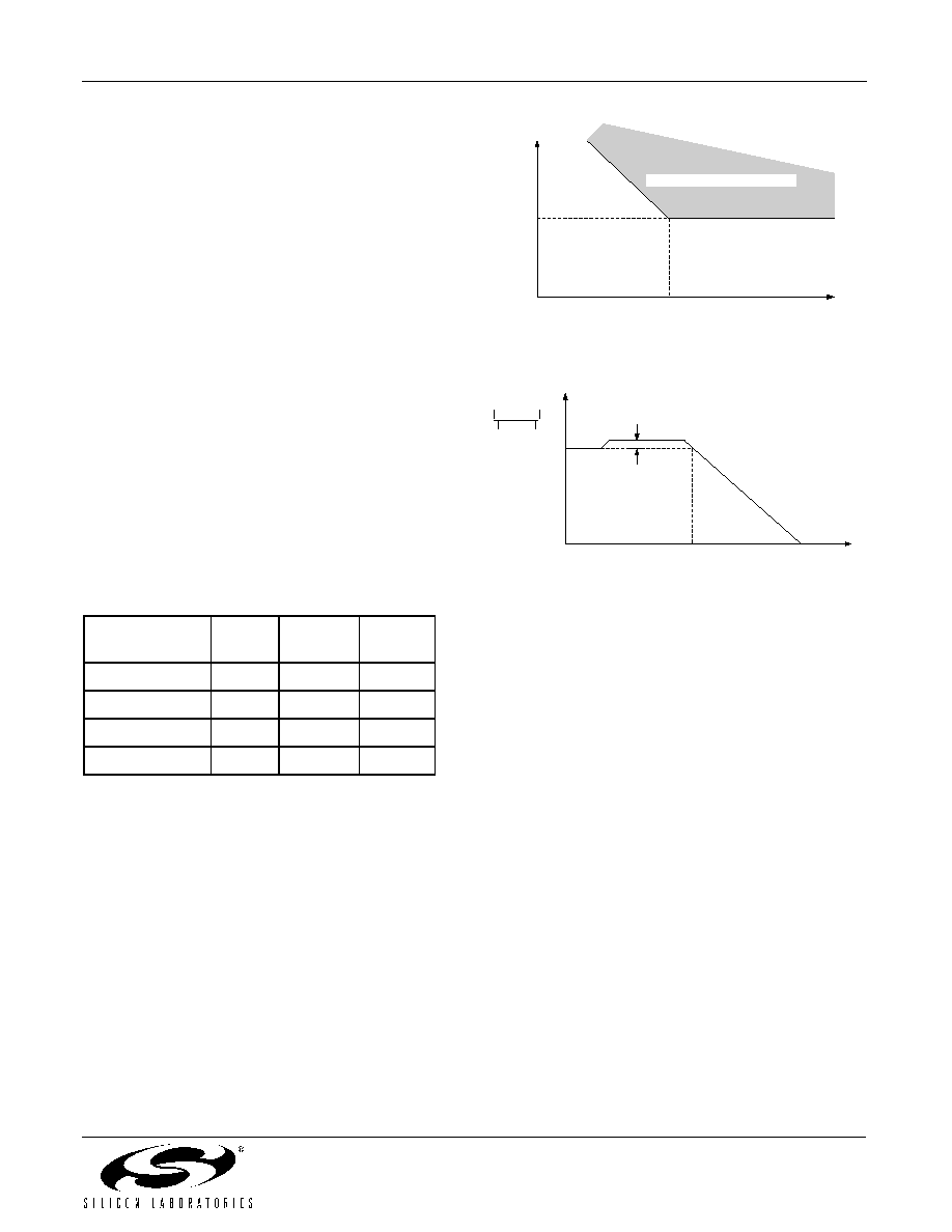
2.2.1. Jitter Tolerance
Jitter tolerance for the Si5364 is defined as the
maximum peak-to-peak sinusoidal jitter that can be
present on the incoming clock. Tolerance is a function of
the input jitter frequency and improves for lower input
jitter frequency.
Figure 8. Jitter Tolerance Mask/Template
Figure 9. PLL Jitter Transfer Mask/Template
2.2.2. Jitter Transfer
Jitter transfer is defined as the ratio of output signal jitter
to input signal jitter for a specified jitter frequency. The
jitter transfer characteristic determines the amount of
input clock jitter that passes to the outputs. The DSPLL
technology used in the Si5364 provides tightly
controlled jitter transfer curves because the PLL gain
parameters are determined by digital circuits that do not
vary over supply voltage, process, and temperature. In
a system application, a well-controlled transfer curve
minimizes the output clock jitter variation from board to
board for consistent system-level jitter performance.
The jitter transfer characteristic is a function of the
BWSEL[1:0] setting. Lower bandwidth selection results
in more jitter attenuation of the incoming clock but might
result in higher jitter generation. Table 4 on page 10
gives the 3 dB bandwidth and peaking values for
specified BWSEL[1:0] settings. Figure 9 shows the jitter
transfer curve mask.
2.2.3. Jitter Generation
Jitter generation is defined as the amount of jitter
produced at the output of the device with a jitter-free
input clock. Jitter is generated from sources within the
VCO and other PLL components. Jitter generation is a
function of the PLL bandwidth setting.
Table 9. FEC Rate Conversion
FEC Frequency
Scaling
FEC1
FEC0
FSYNC
1/1
0
0
Enabled
255/238
0
1
Disabled
238/255
1
0
Enabled
Reserved
1
1
Input
Jitter
Amplitude
10 ns
F
BW
≠20 dB/dec.
f
Jitter In
Excessive Input Jitter Range
Jitter
Transfer
0 dB
F
BW
f
Jitter
Peaking
≠20 dB/dec.
Jitter Out
Jitter In
(s)

Si5364
18
Rev. 2.2
2.3. Frequency Offset and Loss-of-Signal
Alarms
The Si5364 monitors the input clock signals and
provides alarm output signals for frequency offset and
loss-of-signal that is the basis for manual or automatic
clock input switching decisions.
The frequency offset alarms indicate if the CLKIN_A
and CLKIN_B input clocks are within a specified
frequency precision relative to the frequency of the
REF/CLKIN_F input. The REF/CLKIN_F input can also
be utilized as a third clock input for the DSPLL. The
frequency offset monitoring circuitry compares the
frequency of the CLKIN_A and CLKIN_B input clocks
with the frequency of the supplied reference clock (REF/
CLKIN_F). If the frequency offset of an input clock
exceeds a preset frequency offset threshold, a
frequency offset alarm (FOS) is declared for that clock
input. The frequency offset threshold is selectable for
compatibility with either SONET minimum clock (SMC)
or Stratum 3/3E requirements using the SMC/S3N
control input. Frequency offset threshold values are
indicated in Table 3 on page 8.
2.4. Loss-of-Signal
The Si5364 loss-of-signal (LOS) circuitry constantly
monitors the CLKIN_A, CLKIN_B, and REF/CLKIN_F
input clocks for missing pulses. It over-samples the
input clocks to search for extended periods of time
without clock transitions. If the LOS circuitry detects four
consecutive samples of an input clock that are the same
state (i.e., 1111 or 0000), an LOS is declared for that
input clock. The LOS circuitry runs at a frequency of
f
0_622/8
, where f
0_622
is the output clock frequency when
the FRQSEL[1:0] pins are set to 11. Figure 4 on page 6
and Table 3 on page 8 list the minimum and maximum
transitionless time periods required for declaring an
LOS on an input clock.
Once an LOS flag is asserted on one of the input clocks,
it is held high until the input clock is validated over a
time period designated by the VALTIME pin. When
VALTIME is low, the validation time period is about
100 ms. When VALTIME is high, the validation time
period is about 13 s. If another LOS condition on the
same input clock is detected during the validation time
(i.e., if another set of 1111 or 0000 samples are
detected), the LOS flag remains asserted, and the
validation time starts over.
An LOS alarm on the REF/CLKIN_F clock input
automatically disables the FOS_A and FOS_B
frequency offset alarms (frequency offset alarms are
automatically disabled in applications that do not supply
a REF/CLKIN_F input to the Si5364). The FOS_A and
FOS_B frequency offset alarms can be disabled
manually with the DSBLFOS control input.
2.5. Input Clock Select Functions
The Si5364 provides hitless switching between clock
input sources. Switching is controlled automatically or
manually. The criteria for automatic switching are
described below. Automatic switching can be revertive
(returns to the original clock when the alarm condition
clears) or non-revertive. When in manual mode, the
device selects the clock specified by the value of the
MANCNTRL[1:0] inputs.
2.5.1. Hitless Switching
Silicon Laboratories switching technology performs
"phase build-out" to minimize the propagation of phase
transients to the clock outputs during input clock
switching. Many of the problems associated with clock
switching using traditional analog solutions are
eliminated. In the Si5364, all switching between input
clocks occurs within the input multiplexor and DSPLL
phase detector circuitry. The phase detector circuitry
continually monitors the phase difference between each
input clock and the DSPLL VCO clock output. The
phase detector circuitry can lock to a clock signal at a
specified phase offset relative to the VCO output so that
the phase offset is maintained by the DSPLL circuitry. At
the time a clock switch occurs, the phase detector
circuitry knows both the input-to-output phase
relationship for the original input clock and of the new
input clock. The phase detector circuitry locks to the
new input clock at the new clock's phase offset so that
the phase of the output clock is not disturbed. That is,
the phase difference between the two input clocks is
absorbed in the phase detector's offset value, rather
than being propagated to the clock output.
The switching technology virtually eliminates the output
clock phase transients traditionally associated with
clock rearrangement (input clock switching). SONET/
SDH specifications allow transients of up to 150 ns of
maximum time interval error (MTIE) to occur during a
Stratum 2/3E clock switch. This specification, which is
sometimes difficult to meet with analog
implementations, allows for up to 1500 bit periods of slip
to occur in an OC192 data stream. Silicon Laboratories'
switching eliminates these bit slips and the limitations
imposed by analog methods (such as low bandwidth
loops on the port cards) to meet the SONET/SDH
requirements. The MTIE and maximum slope for clock
output phase transients during clock switching with the
Si5364 are given in Table 4 on page 10. These values
fall significantly below the limits specified in the
Telcordia GR-1244-CORE Requirements.
The characteristic of the phase transient specification is
defined in Figure 10. The clock output phase step
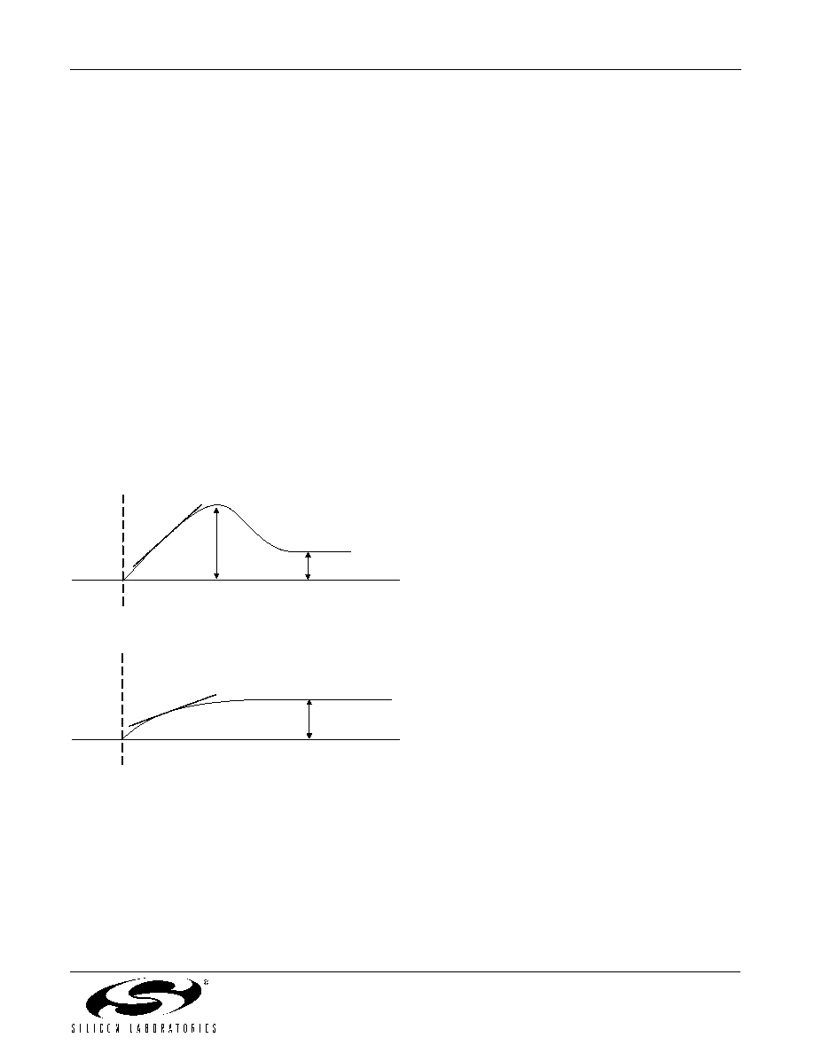
Si5364
Rev. 2.2
19
(t
PT_MTIE
) is the steady-state offset between pre-
switching and post-switching output phases. This
specification applies to both the manual and automatic
switch modes. The clock output phase step slope (M
pt
)
is defined as the rate of change of the output clock
phase during transition. Its magnitude depends on the
setting of the BWSEL[1:0] pins and whether the
switching is triggered manually by users or
automatically by Si5364 due to the changed input
clocks. The maximum transient phase deviation
(t
PT_MTIE_MAX
) only applies to an automatic switch and
is defined as the maximum transient phase disturbance
on the output clock. This transient only occurs in the
automatic mode due to the delay between the actual
loss of the clock and when the LOS detection circuitry
detects the loss. During the delay, the phase detector
measures the phase change of the "lost" clock, and the
DSPLL moves the output clock's phase accordingly.
When the LOS circuitry flags the loss of the clock,
Si5364 switches the reference to the alternate clock.
Since the internal phase monitor circuitry preserves the
phase difference before the event (loss of the original
clock), the output phase is restored, and no excessive
phase deviation is present.
Figure 10. Phase Transient Specification
2.5.2. Automatic Switching
The Si5364 provides automatic and manual control over
which input clock drives the DSPLL. Automatic
switching is selected when the AUTOSEL input is high.
Automatic switching is either revertive (return to the
default input after alarm conditions clear) or non-
revertive (remain with selected input until an alarm
condition exists on the selected input).
The prioritization of clock inputs for automatic switching
is CLKA, followed by CLKB, REF/CLKIN_F, and finally,
digital hold mode. Automatic switching mode defaults to
CLKIN_A at powerup, reset, or when in revertive mode
with no alarms present on CLKIN_A. If a LOS or FOS
alarm occurs on CLKIN_A and there are no active
alarms on CLKIN_B, the device switches to CLKIN_B. If
both CLKIN-A and CLKIN_B are alarmed and REF/
CLKIN_F is present and alarm-free, the device switches
to REF/CLKN_F. If no REF/CLKIN_F is present and
CLKIN_A and CLKIN_B are alarmed, the internal
oscillator digitally holds its last value. If automatic mode
is selected and DSBLFOS is active, automatic switching
is not initiated in response to FOS alarms.
2.5.3. Revertive/Non-Revertive Switching
In automatic switching mode, an alarm condition on the
selected input clock causes an automatic switch to the
highest priority non-alarmed input available. Automatic
switching is revertive or non-revertive, depending on the
state of the RVRT input. In revertive mode, if an alarm
condition on the currently-selected input clock causes a
switch to a lower priority input clock, the Si5364
switches to the original clock input when the alarm
condition is cleared. In revertive mode, the highest
priority reference source that is valid is selected as the
DSPLL input. In non-revertive mode, the current clock
selection remains as long as the selected clock is valid
even if alarms are cleared on a higher priority clock.
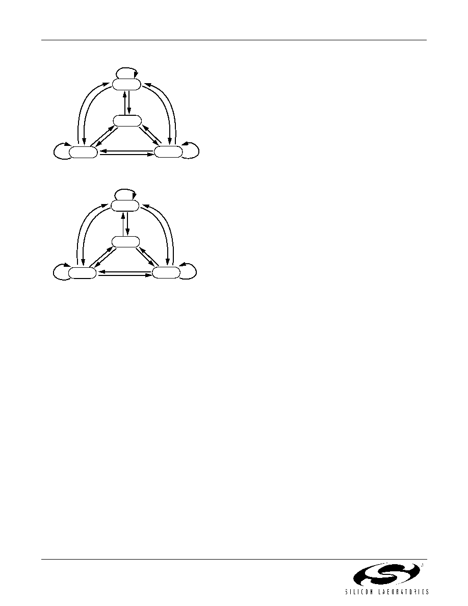
Figure 11 provides state diagrams for revertive mode
switching and for non-revertive mode switching.
m
PT
Loss of Clock
t
PT_MTIE_MAX
t
PT_MTIE
Auto
m
PT
Manual
t
PT_MTIE
Manual
Switch
Si5364
20
Rev. 2.2
.
Figure 11. Si5364 State Diagram for Input
Switching
2.5.4. Manual Switching
Manual switching is selected when the AUTOSEL input
is low and is controlled by the MANCNTRL[1:0] inputs.
When these inputs are set to manually select an input
reference, the DSPLL circuitry locks to the selected
clock. If the selected input is in a LOS alarm state, the
PLL goes into digital hold mode. FOS alarms are
declared according to device specifications but have no
automatic effect on clock selection in manual mode. The
MANCNTRL inputs are ignored when the AUTOSEL
input is high.
2.5.5. Digital Hold of the PLL
In digital hold mode, the Si5364 digitally holds the
internal oscillator at its last frequency value to provide a
stable clock output frequency until an input clock is
again valid. The clock maintains very stable operation in
the presence of constant voltage and temperature. The
frequency accuracy specifications for digital hold mode
are given in Table 4 on page 10.
2.5.6. Hitless Recovery from Digital Hold in Manual
Switching Mode
When operating in manual switching mode with the
Si5364 locked to the selected input clock signal, a loss
of the input clock causes the device to automatically
switch to digital hold mode. If the MANCNTRL[1:0] pins
remain stable (the lost clock is still selected), when the
input clock signal returns, the device performs a hitless
transition from digital hold mode back to the selected
input clock. That is, the device performs "phase build-
out" to absorb the phase difference between the internal
VCO clock operating in digital hold mode and the new/
returned input clock.
The hitless recovery feature can be disabled by
asserting the FXDDELAY pin. When the FXDDELAY pin
is high, the output clock is phase and frequency locked
with a fixed-phase relationship to the input clock.
Consequently, abrupt phase changes on the input clock
will propagate through the device and cause the output
to slew at the selected loop bandwidth until the original
phase relationship is restored.
2.5.7. Clock Input to Clock Output Delay Adjustment
The INCDELAY and DECDELAY pins adjust the phase
of the Si5364 clock outputs. Adjustment is
accomplished by driving a pulse (a transition from low to
high and then back to low) into one of these pins as the
other pin is held at a logic low level.
Each pulse on the INCDELAY pin adds a fixed delay to
the Si5364's clock outputs. The amount of delay time is
equal to twice the period of the 622 MHz output clock
(t
DELAY
= 2/f
O_622
).
Each pulse on the DECDELAY pin removes a fixed
amount of delay from the Si5364's clock outputs. The
fixed delay time is equal to twice the period of the
622 MHz output clock (t
DELAY
= 2/f
O_622
).
The frequency of the 622 MHz output clock (f
O_622
) is
nominally 32x the frequency of the input clock. The
frequency of the 622 MHz output clock (f
O_622
) is scaled
according to the setting of the FEC[1:0] pins.
When the phase of the Si5364 clock outputs is adjusted
using the INCDELAY and/or DECDELAY pins, the
output clock moves to its new phase setting at a rate of
change that is determined by the setting of the
BWSEL[1:0] pins.
Note:
INCDELAY and DECDELAY are ignored when the
Si5364 operates in digital hold (DH) mode.
2.6. 8 kHz Frame Sync
The Si5364 FSYNC output provides a sync pulse output
stream at an 8 kHz nominal rate. The frequency is
derived by dividing down the VCO clock output
A_ACTV=1
B_ACTV=1
F_ACTV=1
DH_ACTV=1
[0,x,x]
[1,0,x]
[1,1,0]
[0,x,x]
[1,0,x]
[0,x,x]
[1,0,x]
[1,1,0]
[1,1,0]
A_ACTV=1
B_ACTV=1
F_ACTV=1
DH_ACTV=1
[0,x,x]
[x,0,x]
[x,x,0]
[0,1,x]
[1,0,x]
[0,x,1]
[1,0,1]
[1,1,0]
[1,1,0]
Non-revertive Mode
Revertive Mode
[1,1,1]
[1,1,1]
[1,1,1]
[1,0,x]
[0,x,x]
[1,1,0]
[1,1,1]
[1,1,1]
[1,1,1]
[0,x,x]
[1,0,x]
[1,1,0]
Notes:
Criteria to determine input switch: [A_fail, B_fail,
LOS_F] where: A_fail = LOS_A or [FOS_A and (not
LOS_F)], B_fail = LOS_B or [FOS_B and (not
LOS_F)]
When entering the DH_ACTV state, the previously
asserted A_ACTV, B_ACTV, or F_ACTV flag
remains asserted.
Si5364
Rev. 2.2
21
frequency. The FSYNC output pulse stream is time
aligned by providing a rising edge on the SYNCIN input
pin. See Figure 3 on page 6. The FSYNC output is
disabled when 255/238 FEC scaling of the clock output
frequencies is selected or when the DSBLFSYNC input
is active.
2.7. Reset
The Si5364 provides a Reset/Calibration pin, RSTN/
CAL, which resets the device and disables the outputs.
When the RSTN/CAL pin is driven low, the internal
circuitry enters into the reset mode, and all LVTTL
outputs are forced into a high impedance state. Also,
the CLKOUT_n+ and CLKOUT_n≠ pins are forced to a
nominal CML logic LOW and HIGH respectively (See
Figure 12). The FRQSEL_n[1:0] setting must be set to
01, 10, or 11 to enable this mode. This feature is useful
for in-circuit test applications. A low-to-high transition on
RSTN/CAL initializes all digital logic to a known
condition and initiates self-calibration of the DSPLL. At
the completion of self-calibration, the DSPLL begins to
lock to the clock input signal.
Figure 12. CLKOUT_n± Equivalent Circuit,
RSTN/CAL asserted LOW
2.8. PLL Self-Calibration
The Si5364 achieves optimal jitter performance by
using self-calibration circuitry to set the VCO center
frequency and loop gain parameters within the DSPLL.
Internal circuitry generates self calibration automatically
on powerup or after a loss-of-power condition. Self-
calibration can also be manually initiated by a low-to-
high transition on the RSTN/CAL input.
Self-calibration should be manually initiated after
changing the state of the FEC[1:0] inputs. Whether
manually initiated or automatically initiated at powerup,
the self-calibration process requires the presence of a
valid input clock.
If the self-calibration is initiated without a valid clock
present, the device waits for a valid clock before
completing the self-calibration. The Si5364 clock output
is set to the lower end of the operating frequency range
while the device waits for a valid clock. After the clock
input is validated, the calibration process runs to
completion, the device locks to the clock input, and the
clock output shifts to its target frequency. Subsequent
losses of the input clock signal do not require re-
calibration. If the clock input is lost following self-
calibration, the device enters digital hold mode. When
the input clock returns, the device re-locks to the input
clock without performing a self-calibration. During the
calibration process, the output clock frequency is
indeterminate and may jump as high as 5% above the
final locked value.
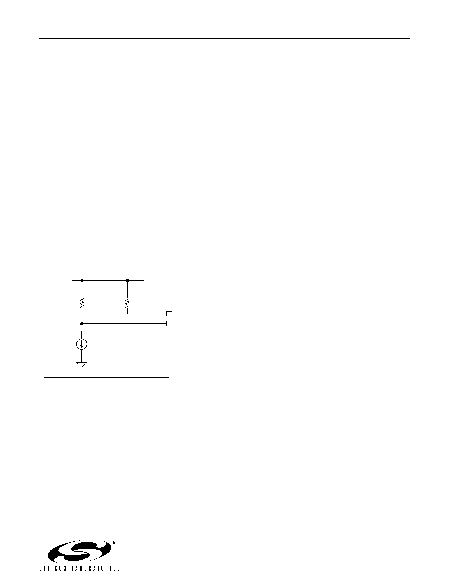
2.9. Bias Generation Circuitry
The Si5364 uses an external resistor to set internal bias
currents. The external resistor generates precise bias
currents that significantly reduce power consumption
and variation compared with traditional implementations
that use an internal resistor. The bias generation
circuitry requires a 10 k
(1%) resistor connected
between REXT and GND.
2.10. Differential Input Circuitry
The Si5364 provides differential inputs for the CLKIN_A,
CLKIN_B, and REF/CLKIN_F clock inputs. These inputs
are internally biased to a voltage of V
ICM
(see Table 2
on page 7) and are driven by differential or single-ended
driver circuits. The termination resistor is connected
externally as shown.
2.11. Differential Output Circuitry
The Si5364 uses current mode logic (CML) output
drivers to provide the clock outputs CLKOUT[3:0]. For
single-ended operation, leave one CLKOUT line
unconnected.
2.12. Power Supply Connections
The Si5364 incorporates an on-chip voltage regulator.
The voltage regulator requires an external
compensation circuit of one resistor and one capacitor
to ensure stability in all operating conditions.
Internally, the Si5364 V
DD33
pins are connected to the
on-chip voltage regulator input, and the V
DD33
pins also
supply power to the device's LVTTL I/O circuitry. The
V
DD25
pins supply power to the core DSPLL circuitry
and are also used for connection of the external
compensation circuit.
The compensation circuit for the internal voltage
regulator consists of a resistor and a capacitor in series
between the V
DD25
node and ground. In practice, if a
100
V
DD
2.5 V
100
CLKOUT_n≠
CLKOUT_n+
15 mA
Si5364
22
Rev. 2.2
capacitor is selected with an appropriate equivalent
series resistance (ESR), the discrete series resistor can
be eliminated. The target RC time constant for this
combination is 15 to 50
µs. The capacitor used in the
Si5364 evaluation board is a 33
µF tantalum capacitor
with an ESR of 0.8
. This gives an RC time constant of
26.4
µs and no discrete resistor is required. (See
Figure 7 on page 15.)
The Venkel part number,
TA6R3TCR336KBR, is an example of a capacitor that
meets these specifications.
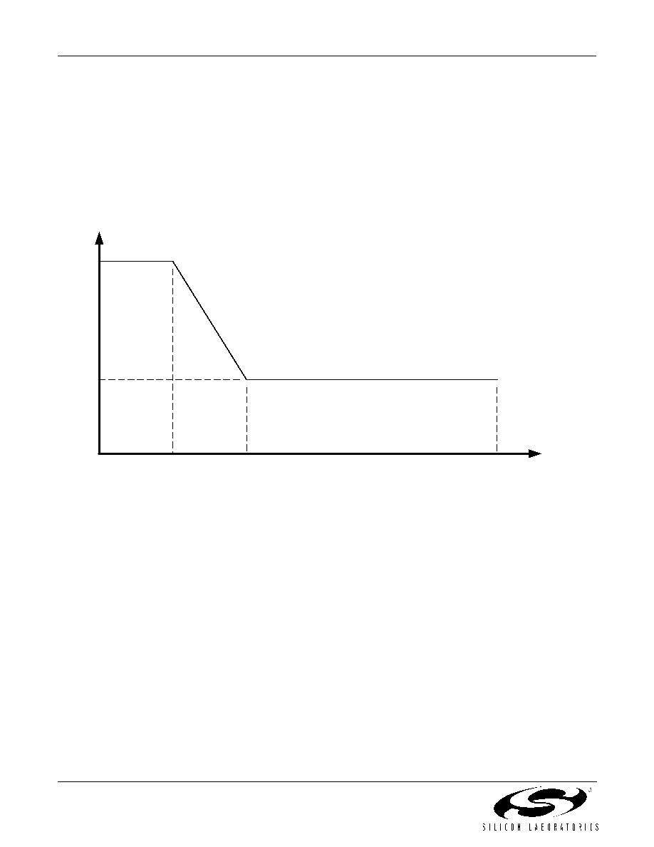
To get optimal performance from the Si5364 device, the
power supply noise spectrum must comply with the plot
in Figure 13. This plot shows the power supply noise
tolerance mask for the Si5364. The customer should
provide a 3.3 V supply that does not have noise density
in excess of the amount shown in the diagram.
However, the diagram cannot be used as spur criteria
for a power supply that contains single tone noise.
Figure 13. Power Supply Noise Tolerance Mask
f
V
n
(µV/Hz)
230
4.5
10 kHz
500 kHz
100 Mhz

Si5364
Rev. 2.2
23
2.13. Design and Layout Guidelines
Precision clock circuits are susceptible to board noise
and EMI. To take precautions against unacceptable
levels of board noise and EMI affecting performance of
the Si5364, consider the following:
Use an isolated, local plane to connect the V
DD25
pins. Avoid running signal traces over or below this
plane without a ground plane in between.
Route all I/O traces between ground planes as much
as possible
Maintain an input clock amplitude in the 200 mV
PP
to
500 mV
PP
differential range.
Excessive high-frequency harmonics of the input
clock should be minimized. The use of filters on the
input clock signal can be used to remove high-
frequency harmonics.
Si5364
24
Rev. 2.2
3. Pin Descriptions: Si5364
Figure 14. Si5364 Pin Configuration (Bottom View)
K
A
B
C
D
E
F
G
H
J
1
10
9
Bottom View
7
8
6
5
4
3
2
Rsvd_G
ND
Rsvd_G
ND
Rsvd_G
ND
Rsvd_G
ND
Rsvd_G
ND
Rsvd_G
ND
Rsvd_G
ND
Rsvd_G
ND
Rsvd_G
ND
Rsvd_G
ND
Rsvd_G
ND
Rsvd_G
ND
Rsvd_G
ND
REXT
RSTN/CAL
CLKOUT_1≠
CLKOUT_1+
GND
CLKOUT_2+
CLKOUT_2≠
VDD25
CLKOUT_3≠
CLKOUT_3+
FSYNC
VALTIME
FRQSEL_1[0]
FRQSEL_1[1]
GND
FRQSEL_2[0]
FRQSEL_2[1]
VDD25
FRQSEL_3[1]
FRQSEL_3[0]
SYNCIN
DSBLFSYNC
GND
GND
GND
GND
GND
VDD25
FRQSEL_4[1]
CLKOUT_4+
CLKIN_B+
CLKIN_B≠
GND
VDD25
VDD25
VDD25
VDD25
VDD25
FRQSEL_4[0]
CLKOUT_4≠
Rsvd_GND
Rsvd_GND
GND
VDD33
VDD33
VDD33
VDD25
VDD25
VDD25
LOS_A
REF/CLKIN_F≠
REF/CLKIN_F+
GND
VDD33
VDD33
VDD33
VDD25
VDD25
VDD25
LOS_B
Rsvd_GND
Rsvd_GND
VSEL33
GND
GND
GND
GND
GND
LOS_F
CLKIN_A≠
CLKIN_A+
INCDELAY
DECDELAY
FXDDELAY
Rsvd_NC
Rsvd_GND
Rsvd_GND
Rsvd_GND
RVRT
AUTOSEL
BWSEL[1]
FEC[1]
MANCNTRL[1]
DSBLFOS
Rsvd_NC
Rsvd_NC
Rsvd_NC
SMC/S3N
CAL_ACTV
BWSEL[0]
FEC[0]
MANCNTRL[0]
FOS_A
FOS_B
A_ACTV
B_ACTV
F_ACTV
DH_ACTV
GND
Si5364
Rev. 2.2
25
Figure 15. Si5364 Pin Configuration (Transparent Top View)
Rsvd_G
ND
Rsvd_G
ND
Rsvd_G
ND
Rsvd_G
ND
Top View
Rs
v
d
_
G
ND
R
svd
_
G
ND
Rsvd_G
ND
Rsvd_G
ND
Rsvd_G
ND
Rsvd_G
ND
Rsvd_G
ND
Rsvd_G
ND
Rsvd_G
ND
Rsvd_G
ND
REXT
RSTN/CAL
CLKOUT_1≠
CLKOUT_1+
GND
CLKOUT_2+
CLKOUT_2≠
VDD25
CLKOUT_3≠
CLKOUT_3+
FSYNC
VALTIME
FRQSEL_1[0] FRQSEL_1[1]
GND
FRQSEL_2[0] FRQSEL_2[1]
VDD25
FRQSEL_3[1] FRQSEL_3[0]
SYNCIN
DSBLFSYNC
GND
GND
GND
GND
GND
VDD25
FRQSEL_4[1] CLKOUT_4+
CLKIN_B+
CLKIN_B≠
GND
VDD25
VDD25
VDD25
VDD25
VDD25
FRQSEL_4[0] CLKOUT_4≠
Rsvd_GND
Rsvd_GND
GND
VDD33
VDD33
VDD33
VDD25
VDD25
VDD25
LOS_A
REF/CLKIN_F≠ REF/CLKIN_F+
GND
VDD33
VDD33
VDD33
VDD25
VDD25
VDD25
LOS_B
Rsvd_GND
Rsvd_GND
VSEL33
GND
GND
GND
GND
GND
GND
LOS_F
CLKIN_A≠
CLKIN_A+
INCDELAY
DECDELAY
FXDDELAY
Rsvd_NC
Rsvd_GND
Rsvd_GND
Rsvd_GND
RVRT
AUTOSEL
BWSEL[1]
FEC[1]
MANCNTRL[1] DSBLFOS
Rsvd_NC
Rsvd_NC
Rsvd_NC
SMC/S3N
CAL_ACTV
BWSEL[0]
FEC[0]
MANCNTRL[0]
FOS_A
FOS_B
A_ACTV
B_ACTV
F_ACTV
DH_ACTV
1
10
9
7
8
6
5
4
3
2
K
A
B
C
D
E
F
G
H
J
Si5364
26
Rev. 2.2
Table 10. Pin Descriptions
Pin #
Pin Name
I/O
Signal Level
Description
C2
C1
CLKIN_A+
CLKIN_A≠
I*
AC Coupled
200≠500 mV
PPD
(See Table 2)
System Clock Input A.
One of three differential clock inputs selected by the
DSPLL when generating the SONET/SDH compliant
clock outputs. The frequencies of the Si5364 clock
outputs are each a 1, 8, or 32x multiple of the fre-
quency of the selected clock input. The multiplication
ratio is selected using Frequency Select (FRQSEL)
control pins associated with each clock output. An
additional scaling factor of either 238/255 or 255/238
is selected for FEC operation using the FEC[1:0]
control pins.
The clock input frequency is nominally 19.44 MHz.
The clock input frequency can be varied over the
range indicated in Table 3 on page 8 to produce
other output frequencies.
CLKIN_A is the highest priority clock input during
automatic switching mode operation.
G1
G2
CLKIN_B+
CLKIN_B≠
I*
AC Coupled
200≠500 mV
PPD
(See Table 2)
System Clock Input B.
One of three differential clock inputs selected by the
DSPLL when generating the SONET/SDH compliant
clock outputs. The frequencies of the Si5364 clock
outputs are each a 1, 8, or 32x multiple of the fre-
quency of the selected clock input. The multiplication
ratio is selected using Frequency Select (FRQSEL)
control pins associated with each clock output. An
additional scaling factor of either 238/255 or 255/238
can be selected for FEC operation using the
FEC[1:0] control pins.
The clock input frequency is nominally 19.44 MHz.
and can be varied over the range indicated in Table 3
on page 8 to produce other output frequencies.
CLKIN_B is the second highest priority clock input
during automatic switching mode operation.
*Note:
The LVTTL inputs on the Si5364 device have an internal pulldown mechanism that causes the input to default to a logic
low state if the input is not driven from an external source.
Si5364
Rev. 2.2
27
E2
E1
REF/CLKIN_F+
REF/CLKIN_F≠
I*
AC Coupled
200≠500 mV
PPD
(See Table 2)
Frequency Reference/Backup Clock Input.
Used by the DSPLL as a frequency reference for
determining the frequency accuracy of the CLKIN_A
and CLKIN_B inputs. If the frequency offset of either
the CLKIN_A or the CLKIN_B inputs relative to REF/
CLKIN_F exceeds the selected frequency offset
threshold, the corresponding Frequency Offset error
flag (FOS_A or FOS_B) is asserted. The frequency
offset threshold is selected with the SMC/S3N input.
In automatic switching mode, Frequency Offset
errors can cause switching of the input clock selec-
tion. (See AUTOSEL pin description.) If the REF/
CLKIN_F signal is not present, the FOS_A and
FOS_B error flags are generated, along with the
LOS_F Loss-of-Signal error flag. The FOS_A and
FOS_B error flags are ignored for the purposes of
automatic switching in the presence of the LOS_F
flag.
The REF/CLKIN_F input can also be utilized as a
third clock input that can be selected by the DSPLL
in the generation of the SONET/SDH compliant clock
outputs. When REF/CLKIN_F is input to the DSPLL
rather than as a frequency accuracy reference for
CLKIN_A and CLKIN_B, the FOS_A or FOS_B fre-
quency offset error outputs can be disabled with the
DSBLFOS control input.
The frequencies of the Si5364 clock outputs are
each a 1, 8, or 32x multiple of the frequency of the
selected clock input. The multiplication ratio is
selected using Frequency Select (FRQSEL) control
pins associated with each clock output. An additional
scaling factor of either 238/255 or 255/238 can be
selected for FEC operation using the FEC[1:0] con-
trol pins.
The clock input frequency is nominally 19.44 MHz.
Clock input frequency can be varied over the range
indicated in Table 3 on page 8 to produce other out-
put frequencies.
F10
LOS_A
O
LVTTL
Loss-of-Signal (LOS) Alarm for CLKIN_A.
Indicates that the Si5364 detects a missing pulse on
the CLKIN_A clock input signal. The LOS alarm is
cleared after either 100 ms or 13 s of valid CLKIN_A
clock input signal, depending on the setting of the
VALTIME control input.
E10
LOS_B
O
LVTTL
Loss-of-Signal (LOS) Alarm for CLKIN_B.
See LOS_A.
Table 10. Pin Descriptions (Continued)
Pin #
Pin Name
I/O
Signal Level
Description
*Note:
The LVTTL inputs on the Si5364 device have an internal pulldown mechanism that causes the input to default to a logic
low state if the input is not driven from an external source.
Si5364
28
Rev. 2.2
D10
LOS_F
O
LVTTL
Loss-of-Signal (LOS) Alarm for REF/CLKIN_F.
See LOS_A.
A5
FOS_A
O
LVTTL
Frequency Offset (FOS) Alarm for CLKIN_A.
Active high output indicates that the frequency offset
between CLKIN_A and REF/CLKIN_F exceeds the
selectable frequency offset threshold. The offset
threshold is selected by the SMC/S3N input. This
output can be disabled with the DSBLFOS control
input.
A6
FOS_B
O
LVTTL
Frequency Offset (FOS) Alarm for CLKIN_B.
See FOS_A.
B9
SMC/S3N
I*
LVTTL
SONET Minimum Clock/Stratum3-3E.
Sets the frequency offset threshold used to trigger
the FOS_A and FOS_B alarm outputs.
0 = 9.2≠16.6 ppm for Stratum 3/3E operation.
1 = 40≠72 ppm for SONET Minimum Clock opera-
tion.
B5
DSBLFOS
I*
LVTTL
Disable FOS.
When high, all frequency offset comparison and error
generation functionality is disabled. When Disable
FOS is active, the FOS_A and FOS_B outputs are
low, and automatic switching is based only on loss-
of-signal (LOS) status.
A4
B4
MANCNTRL[0]
MANCNTRL[1]
I*
LVTTL
Manual Switching Control.
Selects the input clock used by the DSPLL to gener-
ate the SONET/SDH clock outputs. Selection of digi-
tal hold mode locks the current state of the DSPLL
and forces the DSPLL to continue generation of the
output clocks with no additional phase or frequency
information from the input clocks. The MANCNTRL
inputs are internally deglitched to prevent inadvertent
clock switching during changes in the MANCNTRL
state.
The MANCNTRL[1:0] inputs are decoded as follows:
00 = Manual selection of REF/CLKIN_F.
01 = Manual selection of CLKIN_B.
10 = Manual selection of CLKIN_A.
11 = Digital hold mode.
The MANCNTRL inputs are ignored when the
AUTOSEL input is high.
Table 10. Pin Descriptions (Continued)
Pin #
Pin Name
I/O
Signal Level
Description
*Note:
The LVTTL inputs on the Si5364 device have an internal pulldown mechanism that causes the input to default to a logic
low state if the input is not driven from an external source.
Si5364
Rev. 2.2
29
B1
AUTOSEL
I*
LVTTL
Automatic Switching Mode Select.
When 1, the clock input used by the DSPLL to gener-
ate the SONET/SDH clock outputs is selected auto-
matically. The automatic switching mode initially
selects the highest priority clock available, with the
priorities indicated below:
CLKIN_A: Highest Priority
CLKIN_B: Second Highest Priority
REF/CLKIN_F: Lowest Priority
If the selected input clock fails because of an LOS or
FOS alarm condition, the next lower priority clock
that is available is selected.
If an input clock that has a higher priority than the
currently-selected clock becomes available, the
higher priority clock is selected only if RVRT is
active. If RVRT is not active, automatic switching to a
higher priority clock is disabled.
A7
A_ACTV
O
LVTTL
CLKIN_A is Active.
Active high output indicates that CLKIN_A is
selected as the clock input to the DSPLL.
The DH_ACTV output takes precedence over this
signal as an indicator of the DSPLL clock input sta-
tus. When this output is high and the DH_ACTV out-
put is low, CLKIN_A is being used by the DSPLL to
generate the SONET/SDH compatible output clocks.
When this output is high and the DH_ACTV output is
high, CLKIN_A is selected, but the DSPLL is in digi-
tal hold mode. See DH_ACTV.
A8
B_ACTV
O
LVTTL
CLKIN_B is Active.
Active high output indicates that CLKIN_B is
selected as the clock input to the DSPLL.
The DH_ACTV output takes precedence over this
signal as an indicator of the DSPLL clock input sta-
tus. When this output is high and the DH_ACTV out-
put is low, CLKIN_B is being used by the DSPLL to
generate the SONET/SDH compatible output clocks.
When this output is high and the DH_ACTV output is
high, CLKIN_B is selected, but the DSPLL is in
digital hold mode. See DH_ACTV.
Table 10. Pin Descriptions (Continued)
Pin #
Pin Name
I/O
Signal Level
Description
*Note:
The LVTTL inputs on the Si5364 device have an internal pulldown mechanism that causes the input to default to a logic
low state if the input is not driven from an external source.
Si5364
30
Rev. 2.2
A9
F_ACTV
O
LVTTL
REF/CLKIN_F is Active.
Active high output indicates that REF/CLKIN_F is
selected as the clock input to the DSPLL.
The DH_ACTV output takes precedence over this
signal as an indicator of the DSPLL clock input sta-
tus. When this output is high and the DH_ACTV out-
put is low, REF/CLKIN_F is being used by the
DSPLL to generate the SONET/SDH compatible out-
put clocks. When this output is high and the
DH_ACTV output is high, REF/CLKIN_F is selected,
but the DSPLL is in digital hold mode. Refer to
DH_ACTV.
A10
DH_ACTV
O
LVTTL
Digital Hold Mode Active.
Active high output indicates that the DSPLL is in
digital hold mode. Digital hold mode locks the current
state of the DSPLL and forces the DSPLL to
continue generation of the output clocks with no
additional phase or frequency information from the
input clocks.
C10
RVRT
I*
LVTTL
Revertive Switching.
Selects the revertive switching mode during auto-
matic switching operation. If this input is high during
automatic switching, the revertive switching mode is
selected. The highest priority reference source that is
valid is selected as the DSPLL reference source.
See AUTOSEL pin description. During manual mode
of operation, this input has no effect.
K2
RSTN/CAL
I*
LVTTL
Reset/Calibrate.
When low, all outputs are forced into a high-imped-
ance state, the DSPLL is forced out-of-lock, and the
device control logic is reset.
A low-to-high transition on RSTN/CAL initializes all
digital logic to a known condition, enables the device
outputs, and initiates self-calibration of the DSPLL.
At the completion of self-calibration, the DSPLL
begins to lock to the selected clock input signal.
Table 10. Pin Descriptions (Continued)
Pin #
Pin Name
I/O
Signal Level
Description
*Note:
The LVTTL inputs on the Si5364 device have an internal pulldown mechanism that causes the input to default to a logic
low state if the input is not driven from an external source.
Si5364
Rev. 2.2
31
K4
K3
CLKOUT_1+
CLKOUT_1≠
O
CML
Differential Clock Output 1.
High-frequency output clock derived from the
selected reference source (CLKIN_A, CLKIN_B, or
REF/CLKIN_F) or from Digital hold mode.
The frequencies of the Si5364 clock outputs are
each 1, 8, or 32x multiple of the frequency of the
selected clock input. The multiplication ratio is
selected using Frequency Select (FRQSEL) control
pins associated with each clock output. An additional
scaling factor of either 238/255 or 255/238 can be
selected for FEC operation using the FEC[1:0] con-
trol pins.
K6
K7
CLKOUT_2+
CLKOUT_2≠
O
CML
Differential Clock Output 2.
See CLKOUT_1.
K10
K9
CLKOUT_3+
CLKOUT_3≠
O
CML
Differential Clock Output 3.
See CLKOUT_1.
H10
G10
CLKOUT_4+
CLKOUT_4≠
O
CML
Clock Output 4.
See CLKOUT_1.
J3
J4
FRQSEL_1[0]
FRQSEL_1[1]
I*
LVTTL
Frequency Select--Clock Out 1.
Selects the multiplication factor between the fre-
quency of the selected clock input and the frequency
of the clock output.
The FRQSEL_1[1:0] inputs are decoded as follows:
00 = Clock Driver Power Down.
01 = 1x multiplication (19.44 MHz output typical).
10 = 8x multiplication (155.52 MHz output typical).
11 = 32x multiplication (622.08 MHz output typical.
The clock output multiplication ratios can be scaled
additionally by a factor of 255/238 or 238/255 for
FEC operation. See FEC[1:0] pin description.
J6
J7
FRQSEL_2[0]
FRQSEL_2[1]
I*
LVTTL
Frequency Select--Clock Out 2.
See FRQSEL_1[1:0].
J10
J9
FRQSEL_3[0]
FRQSEL_3[1]
I*
LVTTL
Frequency Select--Clock Out 3.
See FRQSEL_1[1:0].
G9
H9
FRQSEL_4[0]
FRQSEL_4[1]
I*
LVTTL
Frequency Select--Clock Out 4.
See FRQSEL_1[1:0].
J1
FSYNC
O
See Table 3
Frame Sync Clock.
Nominally 8 kHz based on a 19.44 MHz reference.
The 8 kHz frame sync is disabled when 255/238 FEC
scaling of the clock output frequencies is selected.
See FEC[1:0] pin description.
Table 10. Pin Descriptions (Continued)
Pin #
Pin Name
I/O
Signal Level
Description
*Note:
The LVTTL inputs on the Si5364 device have an internal pulldown mechanism that causes the input to default to a logic
low state if the input is not driven from an external source.

Si5364
32
Rev. 2.2
H1
SYNCIN
I*
LVTTL
Synchronization Input for Frame Sync Clock.
Allows time alignment/realignment of the FSYNC
output clock. A rising edge on the SYNCIN input
forces alignment of the FSYNC output clock stream.
H2
DSBLFSYNC
I*
LVTTL
Disable the FSYNC Clock Output.
When high, the output driver for the FSYNC pin is
disabled.
A3
B3
FEC[0]
FEC[1]
I*
LVTTL
Forward Error Correction (FEC) Selection.
Enable or disable scaling of the input-to-output fre-
quency multiplication factor for FEC clock rate com-
patibility.
The multiplication ratios and associated frequency
ranges for the Si5364 clock outputs are set by the
FRQSEL pins associated with each clock output.
Additional scaling by a factor of either 255/238 or
238/255 can be applied to all active outputs as indi-
cated below.
The FEC[1:0] inputs are decoded as follows:
00 = No FEC scaling, FSYNC enabled.
01 = 255/238 FEC scaling for all clock outputs,
FSYNC disabled.
10 = 238/255 FEC scaling for all clock inputs,
FSYNC enabled.
11 = Reserved.
The FSYNC output is disabled when FEC[1:0] = 01.
A2
B2
BWSEL[0]
BWSEL[1]
I*
LVTTL
Bandwidth Select.
The BWSEL[1:0] pins set the bandwidth of the loop
filter within the DSPLL to 3200 Hz, 800 Hz, or
6400 Hz as indicated below.
00 = 3200 Hz
01 = 1600 Hz
10 = 800 Hz
11 = 6400 Hz
B10
CAL_ACTV
O
LVTTL
Calibration Mode Active.
Is driven high during the DSPLL self-calibration and
the subsequent initial lock acquisition period.
C7≠9, D1≠2,
F1≠2
Rsvd_GND
--
LVTTL
Reserved--Tie to Ground.
Must be tied to GND for normal operation.
B6≠8, C6
Rsvd_NC
--
LVTTL
Reserved--No Connect.
Must be left unconnected for normal operation.
Table 10. Pin Descriptions (Continued)
Pin #
Pin Name
I/O
Signal Level
Description
*Note:
The LVTTL inputs on the Si5364 device have an internal pulldown mechanism that causes the input to default to a logic
low state if the input is not driven from an external source.
Si5364
Rev. 2.2
33
J2
VALTIME
I*
LVTTL
Clock Validation Time for LOS and FOS.
VALTIME sets the clock validation times for recovery
from an LOS or FOS alarm condition. When VAL-
TIME is high, the validation time is approximately
13 s. When VALTIME is low, the validation time is
approximately 100 ms.
D3
VSEL33
I*
LVTTL
Select 3.3 V V
DD
Supply.
This is an enable pin for the internal regulator. To
enable the regulator, connect this pin to the V
DD33
pins.
E4≠6, F4≠6
V
DD33
V
DD
Supply
3.3 V Supply.
3.3 V power is applied to the V
DD33
pins. Typical
supply bypassing/decoupling for this configuration is
indicated in the typical application diagram for 3.3 V
supply operation.
E7≠9, F7≠9,
G4≠8, H8,
J8, K8
V
DD25
V
DD
Supply
2.5 V Supply.
These pins provide a means of connecting the
compensation network for the on-chip regulator.
D4≠9, E3,
F3, G3, H3≠
7, J5, K5
GND
GND
Supply
Ground.
Must be connected to system ground. Minimize the
ground path impedance for optimal performance of
the device.
K1
REXT
I*
Analog
External Biasing Resistor.
Establishes bias currents within the device. This pin
must be connected to GND through a 10 k
(1%)
resistor.
Table 10. Pin Descriptions (Continued)
Pin #
Pin Name
I/O
Signal Level
Description
*Note:
The LVTTL inputs on the Si5364 device have an internal pulldown mechanism that causes the input to default to a logic
low state if the input is not driven from an external source.

Si5364
34
Rev. 2.2
C3
INCDELAY
I*
LVTTL
Increment Output Phase Delay.
The INCDELAY and DECDELAY pins can adjust the
phase of the Si5364 clock outputs. Adjustment is
accomplished by driving a pulse (a transition from
low to high and then back to low) into one of the pins
while the other pin is held at a logic low level.
Each pulse on the INCDELAY pin adds a fixed delay
to the Si5364's clock outputs. The fixed delay time is
equal to twice the period of the 622 MHz output clock
(t
DELAY
= 2/f
o_622
). The frequency of the 622 MHz
output clock (f
o_622
)
is nominally 32x the frequency of
the input clock. The frequency of the 622 MHz output
clock (fo_622) is scaled additionally according to the
setting of the FEC[1:0] pins.
When the phase of the Si5364 clock outputs is
adjusted using the INCDELAY and/or DECDELAY
pins, the output clock moves to its new phase setting
at a rate of change that is determined by the setting
of the BWSEL[1:0] pins.
Note:
INCDELAY is ignored when the Si5364 is operating
in digital hold (DH) mode.
C4
DECDELAY
I*
LVTTL
Decrement Output Phase Delay.
The INCDELAY and DECDELAY pins can adjust the
phase of the Si5364 clock outputs. Adjustment is
accomplished by driving a pulse (a transition from
low to high and then back to low) into one of the pins
while the other pin is held at a logic low level.
Each pulse on the DECDELAY pin removes a fixed
delay from the Si5364's clock outputs. The fixed
delay time is equal to twice the period of the 622
MHz output clock (t
DELAY
= 2/f
o_622
). The frequency
of the 622 MHz output clock (f
o_622
)
is nominally 32x
the frequency of the input clock. The frequency of the
622 MHz output clock (fo_622) is scaled additionally
according to the setting of the FEC[1:0] pins.
When the phase of the Si5364 clock outputs is
adjusted using the INCDELAY and/or DECDELAY
pins, the output clock moves to its new phase setting
at a rate of change that is determined by the setting
of the BWSEL[1:0] pins.
Note:
INCDELAY is ignored when the Si5364 is operating
in digital hold (DH) mode.
Table 10. Pin Descriptions (Continued)
Pin #
Pin Name
I/O
Signal Level
Description
*Note:
The LVTTL inputs on the Si5364 device have an internal pulldown mechanism that causes the input to default to a logic
low state if the input is not driven from an external source.
Si5364
Rev. 2.2
35
C5
FXDDELAY
I*
LVTTL
Fixed Delay Control.
Active high input that fixes the clock input to clock
output phase relationship to a constant value. When
this pin is high and the device is operating in manual
select mode (AUTOSEL = 0), hitless recovery from
digital hold is disabled, and the input to output phase
relationship will remain fixed as long as the
MANCNTRL[1:0] pins remain unchanged.
This feature is useful in applications that utilize a
single clock source and require a known input-to-
output phase relationship. The FXDDELAY input is
ignored when AUTOSEL is high.
Table 10. Pin Descriptions (Continued)
Pin #
Pin Name
I/O
Signal Level
Description
*Note:
The LVTTL inputs on the Si5364 device have an internal pulldown mechanism that causes the input to default to a logic
low state if the input is not driven from an external source.

Si5364
36
Rev. 2.2
4. Ordering Guide
Part Number
Package
Temperature
Si5364-F-BC
99-Ball CBGA
≠20 to 85 ∞C
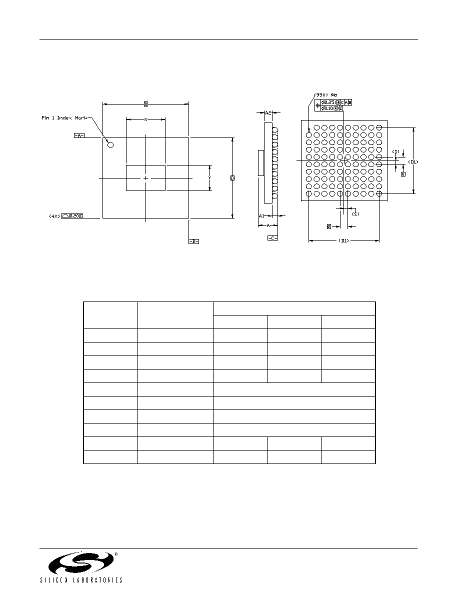
Si5364
Rev. 2.2
37
5. Package Outline
Figure 16 illustrates the package details for the Si5364. Table 11 lists the values for the dimensions shown in the
illustration.
Figure 16. 99-Ball Ceramic Ball Grid Array (CBGA)
Table 11. Package Diagram Dimensions
Symbol
Description
Millimeters
Min
Nom
Max
A
Total Package Height
2.36
2.51
2.66
A1
Standoff
0.65
0.70
0.75
A2
Body Thickness
0.93
1.03
1.13
b
Solder Ball Diameter
0.65
0.70
0.75
D
Body Size
11.00 BSC
D1
Total Array Pitch
9.00 REF
e
Solder Ball Pitch
1.00 BSC
S
Pitch Centerline
0.50 REF
X
Die Length
--
5.22
--
Y
Die Width
--
3.36
--
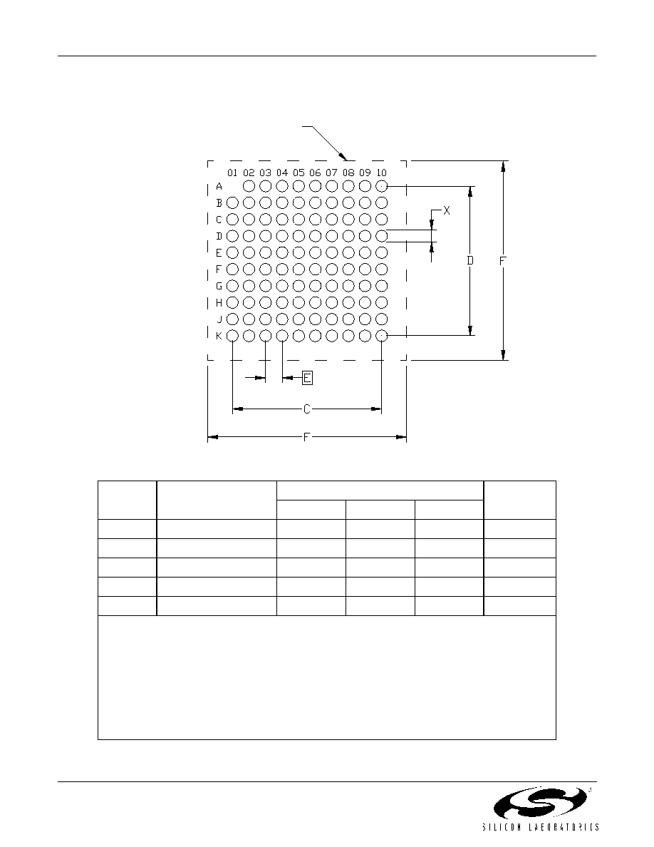
Si5364
38
Rev. 2.2
6. 11x11 mm CBGA Card Layout
Symbol
Parameter
Dimension
Notes
Min
Nom
Max
C
Column Width
--
9.00 REF
--
D
Row Height
--
9.00 REF
--
E
Pad Pitch
--
1.00 BSC
--
F
Placement Courtyard
12.00
--
--
1
X
Pad Diameter
0.64
0.68
0.72
2, 3
Notes:
1.
The Placement Courtyard is the minimum keep-out area required to assure assembly clearances.
2.
Pad Diameter is Copper Defined (Non-Solder Mask Defined/NSMD).
3.
OSP Surface Finish Recommended.
4.
Controlling dimension is millimeters.
5.
Land Pad Dimensions comply with IPC-SM-782 guidelines.
6.
Target solder paste volume per pad is 0.065 mm
3
± 0.010 mm
3
(4000 mils
3
± 600 mils
3
).
Recommended stencil aperture dimensions to achieve target solder paste volume are 0.191 mm
thick x 0.68±0.01 mm diameter, with a 0.025 mm taper.
7.
Recommended stencil type is chemically-etched stainless.
Placement Courtyard

Si5364
Rev. 2.2
39
D
OCUMENT
C
HANGE
L
IST
Revision 2.0 to Revision 2.1
Update Table 3, "AC Characteristics," on page 8.
Updated Figure 10, "Phase Transient Specification,"
on page 19.
Updated Table 11, "Package Diagram Dimensions,"
on page 37.
Added Figure 6, "Typical Si5364 Phase Noise
(CLKIN = 19.44 MHz, CLKOUT = 622.08 MHz, and
Loop BW = 800 Hz)," on page 14.
Revision 2.1 to Revision 2.2
Updated "2.7. Reset" on page 21.
Updated Table 11, "Package Diagram Dimensions,"
on page 37.

Si5364
40
Rev. 2.2
C
ONTACT
I
NFORMATION
Silicon Laboratories Inc.
4635 Boston Lane
Austin, TX 78735
Tel: 1+(512) 416-8500
Fax: 1+(512) 416-9669
Toll Free: 1+(877) 444-3032
Email: productinfo@silabs.com
Internet: www.silabs.com
Silicon Laboratories, Silicon Labs, and DSPLL are trademarks of Silicon Laboratories Inc.
Other products or brand names mentioned herein are trademarks or registered trademarks of their respective holders.
The information in this document is believed to be accurate in all respects at the time of publication but is subject to change without notice.
Silicon Laboratories assumes no responsibility for errors and omissions, and disclaims responsibility for any consequences resulting from
the use of information included herein. Additionally, Silicon Laboratories assumes no responsibility for the functioning of undescribed fea-
tures or parameters. Silicon Laboratories reserves the right to make changes without further notice. Silicon Laboratories makes no warranty,
representation or guarantee regarding the suitability of its products for any particular purpose, nor does Silicon Laboratories assume any
liability arising out of the application or use of any product or circuit, and specifically disclaims any and all liability, including without limitation
consequential or incidental damages. Silicon Laboratories products are not designed, intended, or authorized for use in applications intend-
ed to support or sustain life, or for any other application in which the failure of the Silicon Laboratories product could create a situation where
personal injury or death may occur. Should Buyer purchase or use Silicon Laboratories products for any such unintended or unauthorized
application, Buyer shall indemnify and hold Silicon Laboratories harmless against all claims and damages.