Preliminary Rev. 0.8 3/06
Copyright � 2006 by Silicon Laboratories
Si8250/1/2
This information applies to a product under development. Its characteristics and specifications are subject to change without notice.
Si8250/1/2
D
I G I TA L
P
O W E R
C
O N T R O L L E R
Features
Description
Si8250/1/2 provides all control and protection functions necessary to implement
highly intelligent, fast response power delivery and management control systems
for isolated and non-isolated power supplies. On-board processing capability
enables intelligent control optimization for improved system performance and new
capabilities such as serial connectivity via the PMBus or on-board UART. The
Si8250/1/2 family is in-system Flash programmable enabling control and
protection parameters such as system regulation and protection settings, start-up
and shutdown modes, loop response, and modulation timing to be readily
modified. The built-in high-speed control path provides loop updates every 100nS
and provides pulse-by-pulse current limiting and over-current protection even
while the internal CPU is disabled.
The Si825x family is supported by the Si8250DK development kit, which contains
everything required to develop and program power supply applications with the
Si825x family of digital controllers.
Single-Chip, Flash-based digital
power controller
Supports isolated and non-isolated
applications
Enables new system capabilities
such as:
- Adaptive dead-time control for
higher efficiency
- Nonlinear control for faster
transient response
- Self diagnostics for higher
reliability
- Full PMBus command set
implementation for system
connectivity
Highly integrated control solution:
High-speed digital hardware
control loop
In-system programmable
supervisory processor
Programmable system protection
functions
Hardware cycle-by-cycle current
limiting and OCP
External clock and frame
synchronization inputs
Performs system management
functions such as external power
supply sequencing and fan
control/monitoring
In-system Flash programmable
Flash can also be used as NV
memory for data storage
Low cost, comprehensive
development tool kit includes:
Graphical, easy-to-use system
design tools
Integrated development
environment
In-system, on-line debugger
Turnkey isolated 35 W digital
half-bridge target board
Typical Applications
Isolated and non-isolated DC/DC
converters
AC/DC converters
Fully Pb-free and ROHS compliant
packages
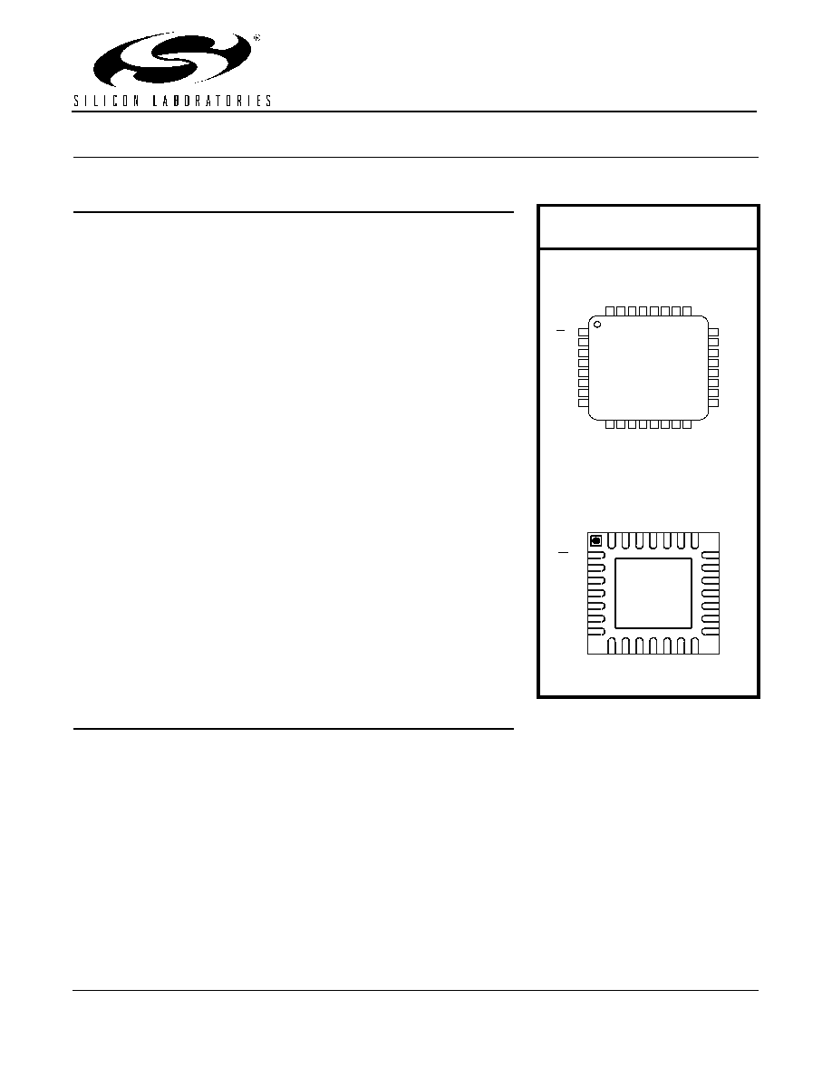
32-pin LQFP
28-pin 5 x 5 mm QFN
Temp Range: �40 to +125 �C
Patents pending
Pin Assignments:
See page 23
4
5
6
7
2
1
3
11
12
13
14
9
8
10
18
17
16
15
20
21
19
25
26
27
28
23
22
24
Si8250/1/2
Top View
RST / C2CK
IPK
VSENSE
GND
VDD
VREF
P1.0/VIN/AIN0
P1
.
1
/A
IN
1
P1
.
2
/A
IN
2
P1
.
3
/A
IN
3
P1
.
4
/A
IN
4
P1
.
5
/A
IN
5
P1
.
6
/A
IN
6
P
1
.
7
/A
IN
7
/
C
2
D
P0.7
P0.6
P0.5
P0.4
P0.3/XCLK
P0.2
P0.1
P0.
0
PH
6
PH
5
PH
4
PH
3
PH
2
PH
1
GND
GND
1
VSENSE
P0.0
P0.5
P0.2
P0.1
P0.3 / XCLK
P1.0/VIN/AIN0
IPK
P0.6
P0.7
2
3
4
5
6
7
8
24
23
22
21
20
19
18
17
9
10
11
12
13
14
15
16
32
31
30
29
28
27
26
25
P0.4
Si8250/1/2
Top View
P1.1/AIN1
GNDA
VDDA
RST/C2CK
GN
D
VD
D
P1
.5/AIN
5
P1
.6/AIN
6
P1.7/AIN
7/
C
2
D
PH
6
PH
5
P1.4/AIN
4
VD
D
GN
D
PH
3
P1.3/AIN
3
P1.2/AIN
2
VREF
PH
4
PH
2
PH
1
28-pin QFN
32-pin LQFP

Si8250/1/2
2
Preliminary Rev. 0.8

Si8250/1/2
Preliminary Rev. 0.8
3
T
A B L E
O F
C
O N T E N TS
Section
Page
1. Electrical Specifications . . . . . . . . . . . . . . . . . . . . . . . . . . . . . . . . . . . . . . . . . . . . . . . . . . .4
2. Benefits of Digital Power Control . . . . . . . . . . . . . . . . . . . . . . . . . . . . . . . . . . . . . . . . . . .14
3. Product Description . . . . . . . . . . . . . . . . . . . . . . . . . . . . . . . . . . . . . . . . . . . . . . . . . . . . . .15
3.1. System Operation . . . . . . . . . . . . . . . . . . . . . . . . . . . . . . . . . . . . . . . . . . . . . . . . . . .16
3.2. Control Processor Functional Block Descriptions (Figure 1) . . . . . . . . . . . . . . . . . . .16
3.3. System Management Processor Functional Block Descriptions . . . . . . . . . . . . . . . .17
4. Design Tools . . . . . . . . . . . . . . . . . . . . . . . . . . . . . . . . . . . . . . . . . . . . . . . . . . . . . . . . . . . .18
5. Example Applications . . . . . . . . . . . . . . . . . . . . . . . . . . . . . . . . . . . . . . . . . . . . . . . . . . . .19
6. Layout Considerations . . . . . . . . . . . . . . . . . . . . . . . . . . . . . . . . . . . . . . . . . . . . . . . . . . .21
7. Pin Descriptions--Si8250/1/2 . . . . . . . . . . . . . . . . . . . . . . . . . . . . . . . . . . . . . . . . . . . . . .23
8. Ordering Guide . . . . . . . . . . . . . . . . . . . . . . . . . . . . . . . . . . . . . . . . . . . . . . . . . . . . . . . . . .25
9. Package Outline--32LQFP . . . . . . . . . . . . . . . . . . . . . . . . . . . . . . . . . . . . . . . . . . . . . . . .26
10. Package Outline--28QFN . . . . . . . . . . . . . . . . . . . . . . . . . . . . . . . . . . . . . . . . . . . . . . . .27
Document Change List . . . . . . . . . . . . . . . . . . . . . . . . . . . . . . . . . . . . . . . . . . . . . . . . . . . . .28
Contact Information . . . . . . . . . . . . . . . . . . . . . . . . . . . . . . . . . . . . . . . . . . . . . . . . . . . . . . . .30
Si8250/1/2
4
Preliminary Rev. 0.8
1. Electrical Specifications
Table 1. Absolute Maximum Ratings*
Parameter
Conditions
Min.
Typ.
Max.
Units
Ambient Temperature under Bias
�55
--
+135
�C
Storage Temperature
�65
--
+150
�C
Voltage on any Port0 Pin with respect to GND
�0.3
--
5.5
V
Voltage on all other pins with respect to GND
�0.3
--
4.0
V
Voltage on VDD with respect to GND
�0.3
--
4.0
V
Maximum total current through VDD or GND
--
--
400
mA
Maximum output current sunk by RST or any
Port pin
--
--
80
mA
*Note: Stresses above those listed under "2.1 Absolute Maximum Ratings" may cause permanent damage to the device. This
is a stress rating only, and functional operation of the devices at those or any other conditions above those indicated in
the operation listings of this specification is not implied. Exposure to maximum rating conditions for extended periods
may affect device reliability.
Table 2. DC Electrical Specifications
TA = �40 to +125 �C, VDD = 2.5 V, SYSCLK = 25 MHz, PLLCLK = 200 MHz unless otherwise specified.
Parameter
Conditions
Min
Typ
Max
Units
Supply Voltage
2.25
--
2.75
V
Supply Current, all Peripherals
Enabled
Analog + digital supply current.
--
26
--
mA
Lockout mode supply current
Analog + digital supply current.
(See Table 1 on page 4)
--
300
--
�A
Digital Supply Current (shutdown)
Oscillator not running, VDD mon-
itor disabled
--
--
TBD
�A
Digital Supply RAM Data Retention
Voltage
--
1.5
--
V

Si8250/1/2
Preliminary Rev. 0.8
5
Table 3. Reference DAC Electrical Specifications
TA = �40 to +125 �C, VDD = 2.5 V, SYSCLK = 25 MHz, PLLCLK = 200 MHz unless otherwise specified.
Parameter
Conditions
Min
Typ
Max
Units
Resolution
--
--
9
Bits
LSB Size
--
2.44
--
mV
Integral Nonlinearity (INL)
�2
--
+2
LSB
Differential Nonlinearity (DNL)
�1.0
--
+1.0
LSB
Settling Time
1/2 LSB change from 0 to
full scale
--
2
--
�s
Turn-on Time
--
20
--
�s
Noise
2 MHz BW
--
1
--
mV
PP
Power Supply Rejection
--
70
--
db
Supply Current
--
220
--
�A
Shutdown Supply Current
--
0.1
--
�A

Si8250/1/2
6
Preliminary Rev. 0.8
Table 4. ADC0 (12-Bit ADC) Specifications
TA = �40 to +125 �C, VDD = 2.5 V, SYSCLK = 25 MHz, PLLCLK = 200 MHz unless otherwise specified.
Parameter
Conditions
Min
Typ
Max
Units
DC Accuracy
Resolution
--
12
--
bits
Integral Nonlinearity
--
--
�2
LSB
Differential Nonlinearity
Guaranteed Monotonic
--
--
�1
LSB
Offset Error
--
�3
--
LSB
Full Scale Error
Differential mode
--
3
--
LSB
Offset Temperature Coefficient
--
TBD
--
ppm/�C
Dynamic Performance (10 kHz sine-wave Single-ended input, 0 to 1 dB below Full Scale, 200 ksps)
Signal-to-Noise Plus Distortion
--
64
--
dB
Total Harmonic Distortion
Up to the 5
th
harmonic
--
83
--
dB
Spurious-Free Dynamic Range
--
�73
--
dB
Conversion Rate
Conversion Time in SAR Clocks
Note 1
--
13
--
clocks
Track/Hold Acquisition Time
Note 2
1
--
--
�s
Throughput Rate
--
--
200
ksps
Analog Inputs
Input Voltage Range
0
--
V
REF
V
Input Capacitance
--
15
--
pF
Temperature Sensor
Linearity
Notes 3, 4
--
�TBD
--
�C
Gain
Notes 3, 4
--
1353
--
�V/�C
Offset
Notes 3, 4 (Temp = 0 �C)
--
488
--
mV
Power Specifications
Power Supply Current (V
DD
sup-
plied to ADC0)
Operating Mode, 200 ksps
--
780
--
�A
Power-On Time
After V
REF
settle, before tracking
begins
--
5
--
�s
Power Supply Rejection
--
TBD
--
mV/V
Notes:
1. An additional 2
F
CLK
cycles are required to start and complete a conversion.
2. Additional tracking time may be required depending on the output impedance connected to the ADC input.
3. Represents one standard deviation from the mean.
4. Includes ADC offset, gain, and linearity variations.
Si8250/1/2
Preliminary Rev. 0.8
7
Table 5. ADC1 Specifications
TA = �40 to +125 �C, VDD = 2.5 V, SYSCLK = 25 MHz, PLLCLK = 200 MHz unless otherwise specified.
Parameter
Conditions
Min
Typ
Max
Units
Sampling Frequency
ADCSP = 0
--
10
--
Msps
ADCSP = 1
--
5
--
Resolution
--
--
6
Bits
LSB Size
4
--
20
mV
Differential Input Voltage Range
Note 1
�32
--
+31
LSB
Common-mode input voltage range
0.8
--
1.3
V
Integral Nonlinearity
�2
--
+2
LSB
Differential Nonlinearity
�1
--
+1
LSB
Gain Error
--
5
--
%
Offset Error
--
3
--
mV
Input Bias Current
--
5
--
�A
Standby Mode Supply Current
disabled
--
0.1
--
�A
Operating Mode Supply Current
--
--
3
mA
Notes:
1. LSB size (mV) is programmable using the RES[3:0] bits in the ADC1CN register.
Table 6. DSP Filter Engine Electrical Specifications
TA = �40 to +125 �C, VDD = 2.5 V, SYSCLK = 25 MHz, PLLCLK = 200 MHz unless otherwise specified.
Parameter
Conditions
Min
Typ
Max
Units
Resolution
1
--
--
9
Bits
Dithering
2
--
--
6
Bits
Standby Mode Supply Current
disabled
--
0.1
--
�A
Notes:
1. Internal word length = 22 bits.
2. Up to a total 15 bits of resolution when dithering is enabled.

Si8250/1/2
8
Preliminary Rev. 0.8
Table 7. Peak Current Limit Detector Electrical Specifications
TA = �40 to +125 �C, VDD = 2.5 V, SYSCLK = 25 MHz, PLLCLK = 200 MHz unless otherwise specified.
Parameter
Conditions
Min
Typ
Max
Units
IPK Input to DPWM Output Latency
10 mV Overdrive
--
45
--
ns
Threshold Detector Voltage
VT[3:0] = 0000
35
50
65
mV
VT[3:0] = 0001
85
100
115
VT[3:0] = 0010
135
150
165
VT[3:0] = 0011
185
200
215
VT[3:0] = 0100
235
250
265
VT[3:0] = 0101
285
300
315
VT[3:0] = 0110
335
350
365
VT[3:0] = 0111
485
400
415
VT[3:0] = 1000
435
450
465
VT[3:0] = 1001
485
500
515
VT[3:0] = 1010
535
550
565
VT[3:0] = 1011
585
600
615
VT[3:0] = 1100
635
650
665
VT[3:0] = 1101
685
700
715
VT[3:0] = 1110
735
750
765
VT[3:0] = 1111
785
800
815
Hysteresis
HYST[1:0] = 00
--
0
--
mV
HYST[1:0] = 01
--
5
--
HYST[1:0] = 10
--
10
--
HYST[1:0] = 11
--
20
--
Blanking Time
LEB[1:0] = 00, f
PLL
= 200 MHz
--
0
--
ns
LEB[1:0] = 01, f
PLL
= 200 MHz
--
20
--
LEB[1:0] = 10, f
PLL
= 200 MHz
--
40
--
LEB[1:0] = 11, f
PLL
= 200 MHz
--
80
--
Input Capacitance
--
4.5
--
pF
Input Bias Current
--
0.1
--
�A
Shutdown Supply Current
Enable bit = 0
--
0.1
--
�A
Active Supply Current
IIN = (Vt + 100 mVpp),
1.5 MHz sq. wave
--
100
--
�A
Si8250/1/2
Preliminary Rev. 0.8
9
Table 8. DPWM Specifications
TA = �40 to +125 �C, VDD = 2.5 V, SYSCLK = 25 MHz, PLLCLK = 200 MHz unless otherwise specified.
Parameter
Conditions
Min
Typ
Max
Units
Clock Frequency
DPWMSP[4:3] = 00
--
--
200
MHz
DPWMSP[4:3] = 01
--
--
50
DPWMSP[4:3] = 1x
--
--
25
Resolution
No dithering
--
--
9
Bits
Dithering enabled
--
--
15
Time Resolution
DPWMSP[4:3] = 00
5
--
--
ns
DPWMSP[4:3] = 01
20
--
--
DPWMSP[4:3] = 1x
40
--
--
SYNC Pulse set-up time
SYNC signal minimum LOW time
before positive transition
3
--
--
DPWM
clock cycles
PH Rise, Fall Time
50pF on pin
--
--
5
ns
Output Resistance High
I
OUT
= �5 mA
--
75
--
Output Resistance Low
I
OUT
= 8 mA
--
40
--
Shutdown Supply Current
--
--
0.1
�A
Table 9. Bandgap Voltage Reference Specs
TA = �40 to +125 �C, VDD = 2.5 V, SYSCLK = 25 MHz, PLLCLK = 200 MHz unless otherwise specified.
Parameter
Conditions
Min
Typ
Max
Units
Output Voltage
--
1.20
--
V
Temperature Stability
�1
--
+1
%
Turn-on Response
(0.01%, 4.7 �F)
--
6.5
--
ms
no load
--
2
--
�s
Noise
4.7 �F --
2
--
�V
(RMS)
Bandgap Current
--
60
--
�A
Reference Buffer Current
--
30
--
�A
Power supply rejection
--
50
--
dB
Si8250/1/2
10
Preliminary Rev. 0.8
Table 10. Comparator0 Specifications
TA = �40 to +125 �C, VDD = 2.5 V, SYSCLK = 25 MHz, PLLCLK = 200 MHz unless otherwise specified.
Parameter
Conditions
Min
Typ
Max
Units
Vin
0
--
V
DD
V
Low-Speed Supply Current
--
8
--
�A
Full-speed Supply Current
--
225
--
�A
Hysteresis
CP0HYP[1:0] = 00
--
0
--
mV
CP0HYP[1:0] = 01
--
7
--
CP0HYP[1:0] = 10
--
14
--
CP0HYP[1:0] = 11
--
28
--
CP0HYN[1:0] = 00
--
0
--
CP0HYN[1:0] = 01
--
�7
--
CP0HYN[1:0] = 10
--
�14
--
CP0HYN[1:0] = 11
--
�28
--
Response Time
Low Power Mode, 25 mV Overdrive
--
180
--
ns
High-Speed Mode, 25 mV Overdrive
--
25
--
Input Capacitance
--
5
--
pF
CMRR
--
50
--
db
Input offset
--
5
--
mV
Si8250/1/2
Preliminary Rev. 0.8
11
Table 11. Reset Electrical Characteristics
TA = �40 to +125 �C, VDD = 2.5 V, SYSCLK = 25 MHz, PLLCLK = 200 MHz unless otherwise specified.
Parameter
Conditions
Min
Typ
Max
Units
RST Output Low Voltage
I
OL
= 8.5mA, VDD = 2.5V
--
--
0.7
V
RST Input High Voltage
0.7 x V
DD
--
--
V
RST Input Low Voltage
--
--
0.3 x V
DD
V
RST Input Pull-up Current
RST = 0.0
--
25
TBD
�A
VDD POR Threshold
2.0
2.1
2.2
V
Missing clock detector timeout
Time from last system clock ris-
ing edge to start of reset
--
250
650
�s
Reset time delay
Delay between release of any
reset source and code execu-
tion at location 0x0000
5.0
--
--
�s
Minimum RST Low time to gen-
erate a System Reset
6.5
--
--
�s
VDD monitor turn-on time
100
--
--
�s
VDD monitor supply current
--
40
--
�A
Table 12. Flash Electrical Characteristics
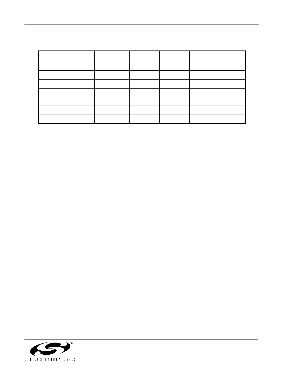
TA = �40 to +125 �C, VDD = 2.25 V � 2.75 V, SYSCLK = 25 MHz, PLLCLK = 200 MHz unless otherwise specified.
Parameter
Conditions
Min
Typ
Max
Units
Flash Size
Si8250
32768
(1)
--
--
bytes
Si8251, Si8252
16383
(1)
--
--
Endurance
10 K
100 K
--
Erase/Write
Read Cycle Time
TBD
--
--
ns
Erase Cycle Time
50 MHz System Clock
32
--
48
ms
Write Cycle Time
50 MHz System Clock
76
--
114
�s
Notes:
1. The last 512 bytes of memory are reserved.
Si8250/1/2
12
Preliminary Rev. 0.8
Table 13. Port I/O DC Electrical Characteristics
TA = �40 to +125 �C, SYSCLK = 25 MHz, PLLCLK = 200 MHz unless otherwise specified.
Parameters
Conditions
Min
Typ
Max
Units
Port0 Input Voltage Tolerance
push-pull
--
--
V
DD
+ 0.7
V
open-drain
--
--
5.5
Port1 Input Voltage Tolerance
--
--
V
DD
+ 0.7
Output High Voltage
I
OH
= �3 mA,
Port I/O push-pull
V
DD
� 0.4
--
--
V
I
OH
= �10 �A,
Port I/O push-pull
V
DD
� 0.1
--
--
I
OH
= �10 mA,
Port I/O push-pull
--
V
DD
� 0.8
--
Output Low Voltage
I
OL
= 8.5 mA
--
--
0.6
V
I
OL
= 10 �A
--
--
0.1
I
OL
= 25 mA
--
1.25
--
Input High Voltage
(0.7) V
DD
--
--
V
Input Low Voltage
--
--
(0.3) V
DD
V
Input Leakage Current
Weak Pullup Off
--
--
�10
�A
Weak Pullup On, V
IN
= 0 V
--
20
50
Table 14. PLL Specifications
TA = �40 to +125 �C, VDD = 2.5 V, SYSCLK = 25 MHz, PLLCLK = 200 MHz unless otherwise specified.
Parameter
Conditions
Min
Typ
Max
Units
Stabilization Time
--
30
--
�s
Input Frequency Range
15
--
25
MHz
PLL Frequency
--
200
--
MHz
Cycle-to-cycle jitter
--
250
--
ps
Supply current
--
15
--
mA
Shutdown current
--
0.1
--
�A
Si8250/1/2
Preliminary Rev. 0.8
13
Table 15. 25MHz Oscillator Specifications
TA = �40 to +125 �C, VDD = 2.5 V, SYSCLK = 25 MHz, PLLCLK = 200 MHz unless otherwise specified.
Parameter
Conditions
Min
Typ
Max
Units
Frequency
--
24.5
--
MHz
Start-up time
--
100
--
�s
Power supply sensitivity
--
0.3
--
%/V
Temperature coefficient
--
50
--
PPM/
�C
Supply current
--
450
--
�A
Shutdown current
--
0.1
--
�A
Table 16. Low Frequency Oscillator (LFO) Specifications
TA = �40 to +125 �C, VDD = 2.5 V, SYSCLK = 25 MHz, PLLCLK = 200 MHz unless otherwise specified.
Parameter
Conditions
Min
Typ
Max
Units
Frequency
--
80
--
kHz
Start-up time
--
100
--
�s
Power supply sensitivity
--
1.7
--
%/V
Temperature coefficient
--
1000
--
PPM/
�C
Supply current
--
4
--
�A
Shutdown current
--
0.1
--
�A

Si8250/1/2
14
Preliminary Rev. 0.8
2. Benefits of Digital Power Control
Digitally controlled power systems have the following
key advantages over analog implementations:
In-system programmability: Virtually all aspects of
digital controller behavior can be changed in
software locally or remotely, and without hardware
modification. This benefits the system in several
ways:
Hardware designs can be segregated into base
platforms (for example, by form factor or output power),
and optimized to the end application in software. This
lowers development costs by reducing the total number
of hardware designs required to address a given
application segment.
The controller's ability to readily accept change makes
possible low-cost, custom power supply versions with
relatively short lead-time.
The cost and risk of field configuration and/or updating
is greatly reduced, lowering the overhead associated
with customer support.
More advanced control algorithms: Power supply
design with fixed-function analog components leads
to many performance trade-offs. For example,
analog compensator design routinely trades stability
for higher loop bandwidth, and places the required
poles and zeros using passive components. The "if-
then-else" decision-making capability of digital
control can change loop bandwidth as needed for
optimum control response. For example the
controller can operate the compensator at a
relatively low bandwidth during steady-state
operation, but significantly extend bandwidth during
a transient. This adaptive response concept can be
applied to improve other operating parameters such
as efficiency.
Power Efficiency Optimization: In a switched mode
power supply, it is desirable to maintain high power
efficiency over a wide range of loads. Software
algorithms can optimize efficiency at every point of
line and load. For example, the software can adjust
dead time with changes load, disable synchronous
rectification at low loads, or take other measures to
maximize efficiency.
Higher operating precision: Switch timing, control
response and protection setting thresholds in analog
systems are typically determined by the values of
external passive components. These components
typically have a wide tolerance and vary with
temperature and time. Designers must allow for
these tolerances when considering worst case
operating conditions. Digital control offers tighter
parameter tolerances with greatly reduced
temperature/time variations resulting in improved
worst-case operating specifications.
Power management and power delivery functions in
a single package: Power management functions,
such as external supply sequencing, PMBus
communication support and fan control can be
performed by the digital controller, eliminating
dedicated external components.
System connectivity: PMBus and other emerging
communication protocols enable system processors
to communicate with the power supply to obtain data
and command action. For example, the system
processor may request the power supply operating
history, perform self-diagnostics or change system
settings without taking the supply off-line.
Communications with the system controller enables
notification of a pending power supply failure,
enhancing system reliability. This attribute also
reduces the cost and complexity of field
configurations and upgrades.
Higher integration/smaller size/lower cost: Many
discrete circuits can be transformed to lines of
software code, eliminating components and saving
cost. The digital controller can be used to execute
self-diagnostic routines during production test
thereby reducing test time and saving cost. The
small physical size of the Si8250 in particular
(5 x 5 mm) saves board space.
Si8250/1/2
Preliminary Rev. 0.8
15
3. Product Description
Figure 1. Functional Block Diagram
Figure 2. Si8250 Top-Level Block Diagram
Si8250/1/2
System Management Processor
I/O (8)
I/O (8)
50MI
PS 8
0
51 CP
U
1280 Byte
RAM
16/32 kB
Flash
PO
RT 0
8
MUX
TEMP
SENSOR
POR
T
1
HARDWARE
DEBUG
RESET
CONTROL
2% 25 Mhz OSC,
and LFO
INTERRUPT
CONTROL
4x 16-BIT
TIMERS
SMBus
3 CH PCA
I/O PORT
LATCHES
ADC
REGISTERS
& LIMIT
DETECTORS
12-BIT
200 Ksps
ADC
UART
AUTO
SCAN
LOGIC
VSENSE
DEBUG
PORT
VDD
SYSCLKIN
Control Processor
IPK
VSENSE
VREF
GATE CONTROL
(6)
MULTIPHASE
DPWM
Pulse-by-Pulse
Current Limiter
and OCP
ICYC
u(n)
10 MHz
ADC
REFDAC
VREF
DSP
FILTER ENGINE
VSENSE
OCP
POWER STAGES
Si8250
System Management Processor
PO
RT
0
I/
O CR
OS
SB
A
R
TEMP
SENSOR
PO
RT
1
50MIPS 8051 CPU
and Memory
Digital Peripherals:
- UART
- SMBus Port
- 4 x 16-Bit Timers
- 3 Ch PCA (PWM)
- I/O Port Latches
VSENSE
DEBUG
PORT
VDD
SYSCLKIN
Control Processor
IPK
VSENSE
VREF
MULTIPHASE
DPWM
Pulse-by-Pulse
Current Limiter
and OCP
ICYC
u(n)
ADC1
10Msps
REFDAC
VREF
DSP
FILTER ENGINE
VSENSE
OCP
ADC 0
12-Bit, 200Ksps
10-Channel
Up to 6 Gate
Control Outputs
GATE
DRIVERS
16 General-Purpose
Analog/Digital I/O Lines
SUPPLY INPUT
VOLTAGE
OUTPUT
FILTER
SWITCHES
AND
MAGNETICS
Analog Input (e.g. average current)
Digital Ouput (e.g. fan speed control)
VOUT
Peak Current Signal (e.g. CT)

Si8250/1/2
16
Preliminary Rev. 0.8
3.1. System Operation
Figure 2 shows the Si8250/1/2 controlling a non-
isolated DC/DC converter operating in digital voltage
mode control. The output voltage signal connects to the
VSENSE input through a resistive divider, limiting the
common mode voltage range applied to ADC1 to a
maximum of VREF. The equivalent resistance of the
divider and the capacitor form an anti-aliasing filter with
a cutoff frequency equal to ADC1 sampling frequency of
divided by 2 (the amplitudes of frequencies above fS/2
must be minimized to prevent aliasing).
Differential ADC1 and the DSP Filter Engine together
perform the same function as an analog error amplifier
and associated RC compensation network. ADC1
digitizes the difference between the scaled output
voltage and a programmable reference voltage provided
by the REFDAC. The ADC1 output signal is frequency
compensated (in digital domain) by the DSP Filter
Engine. The resulting output from the DSP Filter Engine
is a digital code that represents the compensated duty
cycle ratio, u(n). The digital PWM generator (DPWM)
directly varies output timing to the external gate drivers
based on the value of u(n) until the difference between
VSENSE and ADC1 reference level is driven to zero.
Sensing circuitry within the power stages (current
transformer, sense amp, etc.) provides a signal
representative of inductor or transformer current. This
signal connects to the pulse-by-pulse current limiting
hardware in the Si8250/1/2 via the IPK input pin. This
current limiting circuitry is similar to that found in a
voltage mode analog PWM. It contains a fast analog
comparator and a programmable leading-edge blanking
circuit to prevent unwanted tripping of the current
sensing circuitry on the leading edge of the current
pulse. Current limiting occurs when the sensed current
exceeds the programmed threshold. When this occurs,
the on-going active portions of the PWM outputs are
terminated. A programmable OCP counter keeps track
of the number of consecutive current limit cycles, and
automatically shuts the supply down when the
accumulated number of limit cycles exceeds the
programmed maximum.
The System Management Processor is based on a 50
million instruction per second (MIPS) 8051 CPU and
dedicated A/D converter (ADC0). ADC0 digitizes key
analog parameters that are used by the MCU to provide
protection, as well as manage and control other aspects
of the power system. On-board digital peripherals
include: timers, an SMBus interface port (for PMBus or
other protocols); and a universal asynchronous
receiver/transmitter (UART) for serial communications,
useful for communicating across an isolation boundary.
The System Management Processor serves several
purposes, among these are:
1. Continuously optimizes Control Processor operation
(e.g. efficiently optimization)
2. Executes user-specific algorithms (e.g. support for
proprietary system interfaces)
3. Provides regulation for low-bandwidth system
variables (e.g. VIN feed-forward)
4. Performs system fault detection and recovery
5. Provides system housekeeping functions such as
PMBus communication support
6. Manages external device functions (e.g. external
supply sequencing, fan control/monitoring)
The Si8250/1/2 system development requires using the
Si8250DK, a comprehensive development kit providing
all required hardware and software for control system
design. It comes complete with pre-written and verified
application software, and a set of tools that enable the
user to adapt this software to the end application. It also
includes a turnkey isolated half-bridge DC/DC converter
based on the Si8250/1/2 for evaluation and
experimentation.
3.2. Control Processor Functional Block
Descriptions (Figure 1)
ADC 1: Differential input, 10 Msps control loop analog-
to-digital converter. ADC1 digitizes the difference
between the Vsense input and the programmable
voltage reference level from the REFDAC. ADC1 can be
operated at either 5 Msps or 10 Msps and has a
programmable LSB size to prevent limit cycle oscillation
(Limit cycle oscillation can also be avoided using
dithering to increase DPWM resolution). ADC1 has
programmable conversion rates of 10 Msps and 5 Msps
to accommodate a wide loop gain range. ADC1 also
contains a hardware transient detector that interrupts
the CPU at the onset of an output load or unload
transient. The CPU responds by executing specific
algorithms to accelerate output recovery. These
algorithms may include increasing loop bandwidth or
other measures.
REFDAC: 9-bit digital-to-analog converter provides the
output voltage reference setting. The REFDAC uses the
on-board band gap as its voltage reference, or can be
referenced to an external voltage reference source.
REFDAC is used for output voltage calibration,
margining and positioning. The CPU continuously
manages the REFDAC during soft-start and soft-stop.
DSP Filter Engine: This two-stage loop compensation
filter is the functional equivalent of an active RC
compensation in an analog control scheme. The first
filter stage is a PID filter providing one pole and two

Si8250/1/2
Preliminary Rev. 0.8
17
zeros. The second stage is selectable: a two-pole low-
pass filter (LPF) for the fastest possible response, or
SINC (multiple zero) decimation filter for relatively
quieter operation. The PID plus the LPF result in a three
pole, two zero composite filter, while the PID plus the
SINC results in a single pole, multiple zero composite
filter. The SINC filter provides zeros at intervals equal to
f
S
/(2*DEC) where DEC is the decimation ratio (i.e. ratio
of input to output sampling rate). DEC is a software-
programmable parameter, and can be programmed
such that zero placement occurs that the PWM
frequency and its harmonics. This creates more than
100 db attenuation at these frequencies providing lower
system noise levels.
The end-to-end response of the filter is defined using
only six software parameters, and can be re-
programmed during converter operation to implement
nonlinear control response for improved transient
resolution.
As described in the ADC1 section above, limit cycle
oscillation can be avoided by increasing ADC1 LSB size
to allow the DPWM LSB to fit within a single ADC1
output code (i.e. zero-error bin). However in some
applications, it may not be desirable to lower ADC1
sensitivity. For such applications, limit cycle oscillation
can be avoided by dithering the DPWM output. The
DSP Filter Engine contains a pseudo-random,
broadband noise generator - mixing this noise into the
filter output randomly moves the gate control output(s)
over a range of 1 LSB, such that the time-averaged
resolution of the DPWM is increased.
The filter response is programmed using S-domain
design tools included in the Si8250DK development kit,
greatly minimizing software writing tasks.
Pulse-by-pulse Current Limiter/OCP: High-speed
comparator with 4-bit DAC threshold generator and 2-bit
programmable leading-edge blanking delay generator.
The comparator output causes the DPWM to terminate
the on-going portions of the active outputs when the
peak current signal applied to the IPK input exceeds the
threshold setting. Hardware performs an OCP supply
shutdown when the number of consecutive current limit
events equals a programmed maximum.
DPWM: Output generator may be programmed for
pulse width (PWM) or phase-shift modulation using
design tools contained in the Si8250DK design kit. The
DPWM may be modulated by the front-end of the
Control Processor (ADC1 and DSP Filter Engine); or by
the CPU. The DPWM has individually programmable
stop states for supply off (disable) and OCP. Software
bypass mode allows the CPU to force selected outputs
high or low while the remaining outputs continue normal
operation. The DPWM includes an external SYNC input
and ENABLE input, both of which can be connected to
the I/O pins. The Enable is a logic input used to turn the
power supply on and off. It can be configured to be
active high or active low. The SYNC input allows the
start of each switching cycle to be synchronized to an
external clock source, including another Si8250/1/2.
3.3. System Management Processor Func-
tional Block Descriptions
ADC0: Self-sequencing, 10-input, 200 Ksps analog-to-
digital converter. This general-purpose ADC acquires
other analog system parameters for supplemental
control by the CPU (e.g. dead time control using
average input current as the control variable). ADC0
also converts the output of the on-board temperature
sensor. Eight of the ten analog inputs may be
connected to the I/O pins for external interface. The
remaining two analog inputs (Vsense and Temp Sensor)
are internally connected. When placed in Auto
Sequencing mode, ADC0 automatically converts, stores
and limit-checks each analog input, and interrupts the
CPU when a converted result is outside of its
programmed range. This feature greatly facilitates
protection functions because all measurement and
comparison operations are automated.
Temperature Sensor: This sensor measures the die
temperature of the Si8250/1/2. It can achieve 3 C
accuracy with a single-point calibration and 1 C with a
two-point calibration. The temperature output signal is
digitized by ADC0.
8051 CPU: 50MIPS CPU core with 1K of SRAM and up
to 32 kB of Flash memory. This processor has its own
on-board oscillator and PLL, reset sources and real-
time in-system hardware debug interface eliminating the
need for external processor supervisors, timebases,
and "emulators". The CPU has an external interrupt
(INT0/) that can be connected to an external device via
the I/O pins. When interrupted, the CPU suspends
execution of the current task, and immediately vectors
to an interrupt service routine specifically designed to
handle the interrupting device.
Digital peripherals: Peripherals include: four 16-bit
timers, a three-channel programmable counter array
(PCA), each channel useful as a PWM, an SMBus port
useful as a PMBus interface, a UART (useful as a serial
data port for isolated applications, and two 8-bit I/O port
latches for logic control outputs.
Si8250/1/2
18
Preliminary Rev. 0.8
4. Design Tools
The Si8250DK development kit (Figure 3) contains
everything required to develop applications with the
Si825x family of digital power controllers. This kit
supports all phases of power supply development from
controller design through real-time system debugging. It
also includes a turnkey, 35 W isolated DC/DC target
board for evaluation and experimentation.
Figure 3. Si8250DK Development Kit
Figure 4. Software Download to Si8250
Mounted in Power Supply
Figure 5. Timing Design Tool (Top) and Buck
Regulator Compensation Tool (Bottom)
The tool set enables the user to configure pre-written
application software included in the kit to his application
using a set of PC-based graphical user interface (GUIs).
These GUIs (Figure 5) allow the user to quickly and
easily specify and verify system timing, loop
compensation and protection settings, and compile and
download the resulting code into the Si8250/1/2
(Figure 4).
Si8250/1/2
Preliminary Rev. 0.8
19
5. Example Applications
Isolated DC/DC Converter: A 35 W, 400 kHz Si8250-based half bridge converter is shown in Figure 6. This circuit
is the same as that of the target (evaluation) board shipped in the Si8250DK development kit.
Figure 6. Isolated Half-Bridge DC/DC Converter
The Si8250/1/2 is located on the secondary-side of the power supply for optimum transient response. DPWM
outputs PH3 and PH4 control gates of the synchronous rectifiers via a dual driver I.C. DPWM outputs PH1 and
PH2 control the gates of the primary-side switching transistors with isolation provided by a Silicon Laboratories
isolator. A current transformer circuit provides peak current sensing. Primary side analog parameters (input voltage
and current and the filter node voltage) are digitized by a Silicon Laboratories C8051F300 microcontroller and
passed to the Si8250/1/2 using the on-board UART through additional channels of the isolator I.C. to the
Si8250/1/2. The Si8250/1/2 is uses the application software included with the Si8250DK development kit after
being configured for the half-bridge application using the tools supplied in the kit.
When power is applied, the CPU executes an internal reset followed by initialization of all parameters. The
Si8250/1/2 remains in a low-power state, monitoring digitized VIN data from the primary-side MCU until VIN is
within specified limits. At this time, the controller is fully enabled and executes soft-start by monitoring Vout while
sequentially incrementing the loop voltage reference (REFDAC) until the supply output voltage is within specified
range, at which time steady-state operation begins.
During steady-state operation, the MCU operates in interrupt mode where hardware events divert program
execution to specific routines in priority order.
2.2uF
180nH
6 x 100uF
Ceramic
DRIVER
P2
IRLR8113
IRLR8113
180nH
.
0.001
6:1
Si8250
Digital Controller
VOUT
P3
P4
PH4
PH3
P2
P1
10K
3.9K
0.01uF
IPK
Vsense
IOUT
C8051F300
Microcontroller
33K
1K
AIN
RX
Isolator
PH2
PH1
0.010
AIN
1uH
33K
1K
VIN+
1.2nF
120uF
VIN-
GND
VDD
3V3P
IIN
DC BAL
AIN
VIN
2.2uF
TX
4.
7
DRIVER
P1
4.7
0.01uF
4.7
4.7
7.5
~ +
~ -
FDS3572
FDS3572
DRIVER
P3
DRIVER
P4
200
200
3V3P
VDDA
GNDA
3V3P
VDDB
GNDB
GND
VDD
Si8250/1/2
20
Preliminary Rev. 0.8
Single Phase POL (point of load) converter: A 65 W, 400 KHz Si8252 based single phase POL converter block
diagram is shown in Figure 7. DPWM outputs PH1 and PH2 control the gates of the buck and synchronous
switching transistors. A lossless current sensing method that relies on the resistor and inductance of the inductor is
used to measure the current for over current protection. The input voltage is measured using resistor divider
network and analog input port AIN0 of 12bit, 200 kHz ADC0.
Figure 7. Single-phase POL Block Diagram
When power is applied, the CPU executes an internal reset followed by initialization of all parameters. The Si8252
remains in a low-power state, monitoring digitized VIN data until VIN is within specified limits. At this time, the
controller is fully enabled and executes soft-start by monitoring output voltage while sequentially incrementing the
loop voltage reference (REFDAC) until the supply output voltage is within specified range, at which time steady-
state operation begins.
As in the previous half-bridge example, transient response is improved by adjusting loop gain at the onset of a
transient (i.e. nonlinear control). The efficiency of the POL converter can be optimized over the complete load
range by dynamically adjusting the dead-times. Typical efficiency simulation results for the POL are shown in
Figure 8. In this case, the single-phase POL operates at a PWM frequency of 400 kHz with an output voltage of
3.3 V and an input voltage range of 10 to 15 V. The curve shows the efficiency with an input voltage of 12.0 V.
Figure 8. POL Efficiency
PH1
PH2
Vsense
Ipk
DRIVER
DRIVER
VIN
+2.5 V
CIN
GND
Si8252
AIN0
VIN
Vout
LO
AD
Ipk
DIFFERENTIAL
AMPLIFIER
L
C
VDD
Ipk
0
5
10
15
20
25
80
85
90
95
Eff Io
( )
Io
Si8250/1/2
Preliminary Rev. 0.8
21
6. Layout Considerations
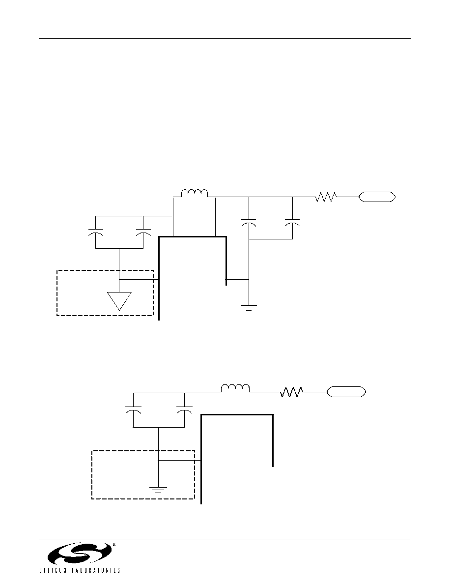
The mixed-signal nature of the Si8250/1/2 mandates clean bias supplies and ground returns. It is best to provide
separate ground planes for analog, digital and power switch returns. These planes should tie together at only one
point to eliminate the possibility of circulating ground currents.
For best performance, the VDD supply should be decoupled from the main supply. The LQFP-32 package provides
the best noise performance because it has separate analog and digital VDD and ground inputs (AVDD, AGND). As
shown in Figure 9, the AVDD is decoupled by a filter consisting of a 1
resistor in series with a 500 mA, 40
ferrite bead and a parallel combination of a 10 uF with a 0.1 uF high-frequency bypass capacitor. All connections
should be kept as short as possible. The VDDA and GNDA should be connected into their respective ground
planes. The QFN-28 package shares analog and digital power with ground on the same pins. Power supply
decoupling is shown in Figure 10. Again, all connections should be kept as short as possible.
Figure 9. Power Supply Connections for LQFP-32 Package
Figure 10. Power Supply Connections for QFN-28 Package
AVDD
DVDD
Ferrite bead
500 mA, 40
0.1 uF
10 uF
Si8250/1/2
AGND
DGND
AGND
10 uF
0.1 uF
2.5 V
1
Keep trace
lengths as short
as possible
VDD
Ferrite bead
500 mA, 40
0.1 uF
10 uF
Si8250/1/2
GND
2.5 V
1
Keep trace
lengths as short
as possible
Si8250/1/2
22
Preliminary Rev. 0.8
In both cases, the bias supplies must be filtered using low ESR/ESL capacitors placed close to the IC pins.
Thick copper traces should be connected to the bias pins (VDD, VDDA) and the ground pins (GND, GNDA) to
reduce resistance and inductance. The copper routings from the drivers to the FETs should be kept short and wide,
especially in very high frequency applications, to reduce inductance of the traces so that the drive signals can be
kept clean.
Connections between VSENSE and the output voltage must be kept absolutely as short as possible to minimize
inductance and parasitic ringing effects. It is best to locate the Si8250/1/2 as close to the output voltage terminal as
possible and use a Kelvin connection to ensure to difference in ground potential between the Si8250/1/2 and the
output voltage ground return.
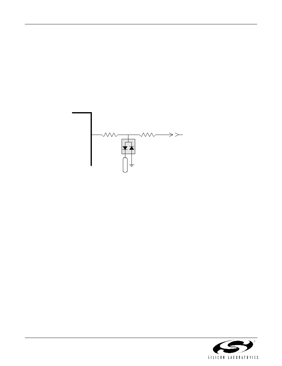
Most applications will require access to the debug pins. These pins are susceptible to damage from electrostatic
discharge (ESD). It is therefore recommended the debug circuit interface use the input protection circuitry shown in
Figure 11.
Figure 11. Debug Interface Pin Protection Circuit
DEBUG
CONNECTOR
10
10
Si8250/1/2
Debug Pins
(C2D, C2CK)
2.
5 V
Si8250/1/2
Preliminary Rev. 0.8
23
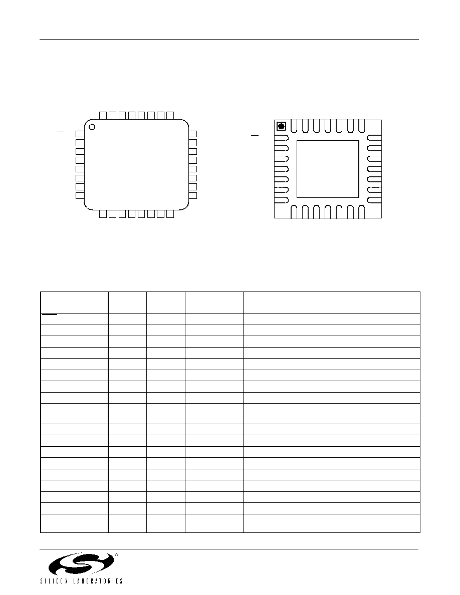
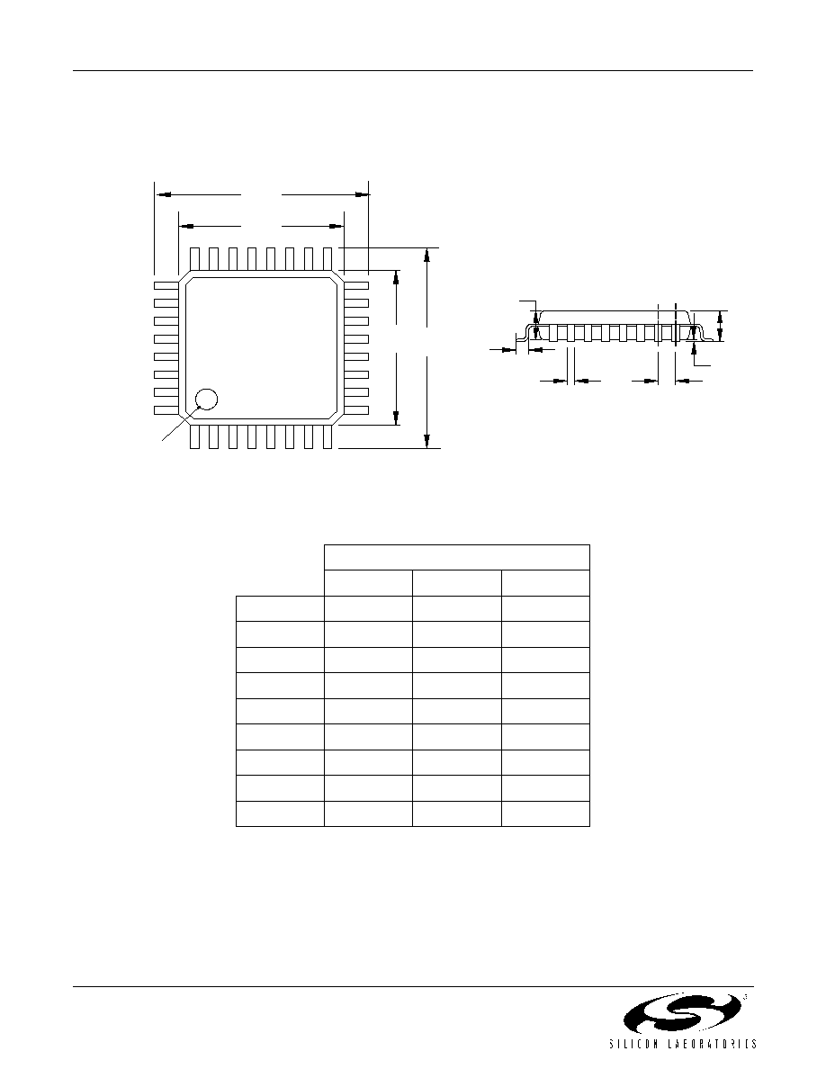
7. Pin Descriptions--Si8250/1/2
Figure 12. Example Pin Configurations
Table 17. Pin Descriptions
Name
QFN-28
Pin #
LQFP-32
Pin#
Type
Description
RST/C2CK
1
1
D I/O
Reset input or bidirect debug clock
IPK
2
2
AIN
Inductor current input
VSENSE
3
3
AIN
Output voltage feedback input
GND
4
--
AIN
Ground
GNDA
--
4
AIN
Ground
VDD
5
--
AIN
Power supply input
VDDA
--
5
AIN
Power supply input
VREF
6
6
AIN
External voltage reference input
P1.0/VIN or AIN0
7
7
D I/O or AIN
Port 1 I/O or scaled power supply input voltage or
ADC input 0
P1.1/AIN1
8
8
D I/O or AIN
Port 1 I/O or ADC input 1
P1.2/AIN2
9
9
D I/O or AIN
Port 1 I/O or ADC input 2
P1.3/AIN3
10
10
D I/O or AIN
Port 1 I/O or ADC input 3
P1.4/AIN4
11
11
D I/O or AIN
Port 1 I/O or ADC input 4
GND
--
12
AIN
Ground
VDD
--
13
AIN
Power supply input
P1.5/AIN5
12
14
D I/O or AIN
Port 1 I/O or ADC input 5
P1.6/AIN6
13
15
D I/O or AIN
Port 1 I/O or ADC input 6
P1.7/ AIN7/C2D
14
16
D I/O, DIN or
AIN
Port 1 I/O or ADC input 7 or C2 Data
32-pin LQFP
28-pin QFN
1
VSENSE
P0.0
P0.5
P0.2
P0.1
P0.3 / XCLK
P1.0/VIN/AIN0
IPK
P0.6
P0.7
2
3
4
5
6
7
8
24
23
22
21
20
19
18
17
9
10
11
12
13
14
15
16
32
31
30
29
28
27
26
25
P0.4
Si8250/1/2
Top View
P1.1/AIN1
GNDA
VDDA
RST/C2CK
GN
D
VD
D
P
1
.5/A
IN5
P
1
.6/A
IN6
P
1
.7/A
IN7/C2D
PH6
PH5
P
1
.4
/A
IN
4
VDD
GND
PH3
P
1
.3
/A
IN
3
P
1
.2
/A
IN
2
VREF
PH4
PH2
PH1
4
5
6
7
2
1
3
11
12
13
14
9
8
10
18
17
16
15
20
21
19
25
26
27
28
23
22
24
Si8250/1/2
Top View
RST / C2CK
IPK
VSENSE
GND
VDD
VREF
P1.0/VIN/AIN0
P1
.1
/AI
N
1
P1
.2
/AI
N
2
P1
.3
/AI
N
3
P1
.4
/AI
N
4
P1
.5
/AI
N
5
P1
.6
/AI
N
6
P
1
.7
/AI
N
7/
C2
D
P0.7
P0.6
P0.5
P0.4
P0.3/XCLK
P0.2
P0.1
P0
.0
PH6
PH5
PH4
PH3
PH2
PH1
GND
GND
Si8250/1/2
24
Preliminary Rev. 0.8
Pin Functions:
RST/C2CK: CPU reset or debug tool clock. Driving this pin low resets the CPU. This pin is also clocked by the USB
debug adaptor during debug.
IPK: Input to the peak current detector for pulse-by-pulse current limiting and over-current protection shutdown
control.
VSENSE: ADC1 inverting input. This is the voltage feedback input for the Si8250. The maximum allowable signal is
VREF.
GND: Digital ground for the 32LQFP package, and the main ground for the 28MLP package.
GNDA: Analog ground for 32LQFP only.
VDD: Digital supply voltage for the 32LQFP package, and main supply voltage for the 28MLP package.
VDDA: Analog supply for 32LQFP only.
P1.0/VIN or AIN0: Programmable multifunction I/O pin. This pin can be software configured to be either a Port 1
digital input or output, or an ADC0 input at AMUX address 0. If used in a non-isolated application, positive input
supply voltage must be tied to this input through a resistor divider and anti-aliasing capacitor to minimize the
frequencies above fS/2 (100Khz) to prevent aliasing. Isolated applications may use this input as general-purpose
digital I/O or analog input.
P1.1 or AIN1�P1.7 or AIN7: Programmable multifunction I/O pins. These pins can be software configured to be a
Port 1 digital input or output, or an ADC0 input. P1.7 also serves as the debug data input (C2D) and is used during
debug by the USB debug adaptor. P1.7 may be used as general-purpose digital I/O when not in debug mode. Any
of the digital peripherals may be programmed to connect to these pins.
P0.0�P0.7: Programmable multifunction I/O pins. These pins can be software configured to be either a Port 1
digital input or output, or an ADC0 input. Any of the digital peripherals (including the ENABLE input) may be
programmed to connect to these pins. P0.3 may be programmed to serve as an external (25MHz nominal) clock
input.
PH1�PH6: DPWM gate control (complementary drive) outputs. These signals connect to the MOSFET gates
through an external gate driver. The output levels swing between ground and Vdd.
P0.7
15
17
D I/O
Port 0 I/O
P0.6
16
18
D I/O
Port 0 I/O
P0.5
17
19
D I/O
Port 0 I/O
P0.4
18
20
D I/O
Port 0 I/O
P0.3/XCLK
19
21
D I/O
Port 0 I/O
P0.2
20
22
D I/O
Port 0 I/O
P0.1
21
23
D I/O
Port 0 I/O
P0.0
22
24
D I/O
Port 0 I/O or bidirectional debug data
PH6
23
25
DOUT
Phase 6 switch control output
PH5
24
26
DOUT
Phase 5 switch control output
PH4
25
27
DOUT
Phase 4 switch control output
VDD
--
28
AIN
Power supply input
GND
--
29
AIN
Ground
PH3
26
30
DOUT
Phase 3 switch control output
PH2
27
31
DOUT
Phase 2 switch control output
PH1
28
32
DOUT
Phase 1 switch control output
Table 17. Pin Descriptions (Continued)
Name
QFN-28
Pin #
LQFP-32
Pin#
Type
Description
Si8250/1/2
Preliminary Rev. 0.8
25
8. Ordering Guide
Ordering Number
Flash Memory
Number of
PWM
Outputs
UART
Package
Si8250-IQ
32 kB
6
Yes
LQFP-32
Si8250-IM
32 kB
6
Yes
QFN-28
Si8251-IQ
16 kB
6
Yes
LQFP-32
Si8251-IM
16 kB
6
Yes
QFN-28
Si8252-IQ
16 kB
3
No
LQFP-32
Si8252-IM
16 kB
3
No
QFN-28
Si8250/1/2
26
Preliminary Rev. 0.8
9. Package Outline--32LQFP
Figure 13 illustrates the package details for the 32-pin LQFP version of the Si8250/1/2. Table 18 lists the values for
the dimensions shown in the illustration.
Figure 13. 32-pin LQFP Package Diagram
Table 18. LQFP-32 Package Dimensions
MM
Min
Typ
Max
A
--
--
1.60
A1
0.05
--
0.15
A2
1.35
1.40
1.45
b
0.30
0.37
0.45
D
--
9.00
--
D1
--
7.00
--
e
--
0.80
--
E
--
9.00
--
E1
--
7.00
--
PIN 1
IDENTIFIER
A1
e
b
1
32
E1
D1
D
E
A2
A
L
Si8250/1/2
Preliminary Rev. 0.8
27
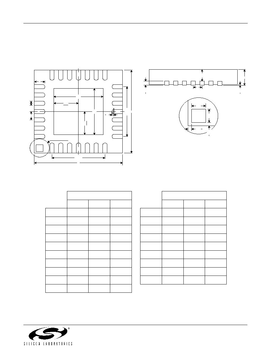
10. Package Outline--28QFN
Figure 14 illustrates the package details for the 28-lead QFN version of the Si8250/1/2. Table 19 lists the values for
the dimensions shown in the illustration.
Figure 14. 28-lead Quad Flat No-lead (QFN) Package Diagram
Table 19. QFN-28 Package Dimensions
MM
MM
Min
Typ
Max
Min
Typ
Max
A
0.80
0.90
1.00
L
0.45
0.55
0.65
A1
0
0.02
0.05
N
--
28
--
A2
0
0.65
1.00
ND
--
7
--
A3
--
0.25
--
NE
--
7
--
b
0.18
0.23
0.30
R
0.09
--
--
D
--
5.00
--
AA
--
0.435
--
D2
2.90
3.15
3.35
BB
--
0.435
--
E
--
5.00
--
CC
--
0.18
--
E2
2.90
3.15
3.35
DD
--
0.18
--
e
--
0.5
--
1
E
D
A2
A
A1
e
A3
E2
R
e
L
Bottom View
Side View
2
3
4
5
6
7
8
9
10
12
13
14
21
20
19
17
16
15
28
27
26
24
23
22
E2
25
2
D2
11
18
D2
2
6 x e
6 x e
DETAIL 1
DETAIL 1
AA
BB
CC
DD
b

Si8250/1/2
28
Preliminary Rev. 0.8
D
OCUMENT
C
HANGE
L
IST
Revision 0.7 to Revision 0.8
Updated DPWM phase output drive-high and drive-
low resistance in Table 8, "DPWM Specifications," on
page 9.

Si8250/1/2
Preliminary Rev. 0.8
29
N
OTES
:

Si8250/1/2
30
Preliminary Rev. 0.8
C
ONTACT
I
NFORMATION
Silicon Laboratories Inc.
4635 Boston Lane
Austin, TX 78735
Tel: 1+(512) 416-8500
Fax: 1+(512) 416-9669
Toll Free: 1+(877) 444-3032
Email: productinfo@silabs.com
Internet: www.silabs.com
Silicon Laboratories and Silicon Labs are trademarks of Silicon Laboratories Inc.
Other products or brandnames mentioned herein are trademarks or registered trademarks of their respective holders.
The information in this document is believed to be accurate in all respects at the time of publication but is subject to change without notice.
Silicon Laboratories assumes no responsibility for errors and omissions, and disclaims responsibility for any consequences resulting from
the use of information included herein. Additionally, Silicon Laboratories assumes no responsibility for the functioning of undescribed features
or parameters. Silicon Laboratories reserves the right to make changes without further notice. Silicon Laboratories makes no warranty, rep-
resentation or guarantee regarding the suitability of its products for any particular purpose, nor does Silicon Laboratories assume any liability
arising out of the application or use of any product or circuit, and specifically disclaims any and all liability, including without limitation conse-
quential or incidental damages. Silicon Laboratories products are not designed, intended, or authorized for use in applications intended to
support or sustain life, or for any other application in which the failure of the Silicon Laboratories product could create a situation where per-
sonal injury or death may occur. Should Buyer purchase or use Silicon Laboratories products for any such unintended or unauthorized ap-
plication, Buyer shall indemnify and hold Silicon Laboratories harmless against all claims and damages.