
1000
10000
0
1
2
3
4
5
6
7
8
9
10
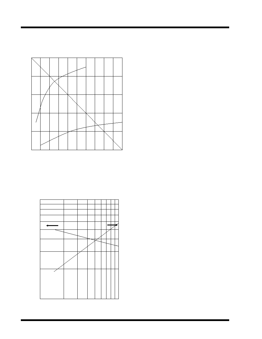
MAXIMUM ON-STATE CHARACTERISTIC
Initial TJ=105 degC / 8ms pulse
On-state current , It (amperes)
On-state Voltage , Vt (volts)
On-state Voltage , Vt (volts)
30000
100mm
100mm
100mm
100mm
100mm THYRIST
THYRIST
THYRIST
THYRIST
THYRISTOR PRESSP
OR PRESSP
OR PRESSP
OR PRESSP
OR PRESSPA K
A K
A K
A K
A K
6000V / 2100A
6000V / 2100A
6000V / 2100A
6000V / 2100A
6000V / 2100A
Type C792 thyristor is suitable for phase control applications such as for HVDC valves,static VAR
compensators and synchronous motor drives. The silicon junction design utilizes a second generation
pilot gate and a unique orientation of emitter shorts which promote the lateral expansion of conducting
plasma resulting in lower spreading losses while achieving high dv/dt withstand. It is supplied in an
industry accepted disc-type package,ready to mount using commercially available heat dissipators and
mechanical clamping hardwar
e.
REPETITIVE PEAK REVERSE
AND OFF-STATE BLOCKING
V O L T A G E
T
J
= 0 to 115
o
C
M O D E L
V
D R M
V
R R M
(volts)
(volts)
C792FP
6000
6000
C792ET
5900
5900
C792EN
5800
5800
C792ES
5700
5700
C792EM
5600
5600
C792EE
5500
5500
MECHANICAL OUTLINE
C792
C792
C792
C792
C792
175 GREAT VALLEY PKWY. MALVERN, PA 19355
U S A
ELECTRICAL
CREEPAGE / STRIKE
1.6 / 1.0 in
40.6 / 25.4 mm
CLAMPING FORCE
(range)
17000-19000 lb.
11/13/01
B ÿ
B ÿ
A ÿ
2 0∞ ±5 ∞
D
CL
CL
J
A
A
A
A
A F
F
F
F
F = 5.65 in (143.5 mm)
= 5.65 in (143.5 mm)
= 5.65 in (143.5 mm)
= 5.65 in (143.5 mm)
= 5.65 in (143.5 mm)
B
B
B
B
B F
F
F
F
F =3.92 in (99.4 mm)
=3.92 in (99.4 mm)
=3.92 in (99.4 mm)
=3.92 in (99.4 mm)
=3.92 in (99.4 mm)
D=1.45 in (36.8 mm)
D=1.45 in (36.8 mm)
D=1.45 in (36.8 mm)
D=1.45 in (36.8 mm)
D=1.45 in (36.8 mm)
0.001
0.01
0.1
1
10
Zthj-case (degC/watt)
Power On-time (seconds)
Power On-time (seconds)
o1a:t305tau
.0001
.001
.01
Rthj-c=.005 degC/W
add .002 for
case to sink

P2 / 11/13/01
LIMITING CHARACTERISTICS AND RATINGS
TEST
M A X I M U M
PARAMETER
S Y M B O L
CONDITIONS
VALUES
UNIT S
Repetitive peak off-
V
D R M
T
j
=0
see
V
state and reverse
V
R R M
to +115
o
C
table
voltage
Repetitive working
V
D W M
T
j
=0
.8V
D R M
V
crest voltage
V
D R M
to 115
o
C
.8V
R R M
Rep.off-state and
I
D W M
V
D W M
150
ma
reverse leakage
I
R R M
V
R W M
150
ma
current
T
j
=115
o
C
On-state Voltage
V
T M
I
T
=2000A
1.90
V
t
p
=8.3ms
T
j
=115
o
C
Critical DC gate
I
G T
V
D
=12VDC
150
ma
current/voltage
V
G T
T
j
=25
o
C
3
V
to trigger on
Non-trigger gate
I
G D
V
D
=.8V
D R M
8
ma
current/voltage
V
G D
T
J
=115
o
C
_
V
Critical rate of
dv/dt
0.67V
D R M
2000
V/us
rise of off-state
T
j
=115C
Critical rate of
di/dt
rep
0.67 V
D R M
100
A/us
of on-state
see req'd gating
Peak recovery
I
RM(rec)
di/dt=2A/us
118
A
current
T
j
=115
o
C
Peak half-cycle
I
T S M
t
p
=8.3ms
35
kA
non-repetitive
t
p
=10 ms
34
surge current
Circuit commutated
t
q
di/dt=5A/us
600
us
turn-off time
dv/dt=20V/us
GATE CIRCUIT REQUIREMENTS
Open circuit voltage
40 - 50 V
Short circuit current
3 A minimum
Current risetime
0.5 us nominal
Pulse duration
10-20 us
C792 / 6RT300

0
500
1000
1500
2000
2500
3000
3500
4000
4500
0
1
2
3
4
5
6
FULL CYCLE AVERAGE POWER DISSIPATION
Sine Wave-includes spread loss
Avg.Power,Pavg (watts)
Peak Current , It (kA)
Peak Current , It (kA)
6RT300
conduction angle (degrees)
180
150
120
90
60
30
0
500
1000
1500
2000
2500
3000
3500
4000
4500
5000
U = 10 deg
U = 20
U = 40
0
0.5
1
1.5
2
2.5
3
3.5
4
4.5
5
FULL CYCLE AVERAGE POWER DISSIPATION
120-Deg Conduction-includes spread loss
as a function of overlap angle ,U
Avg.Power(watts)
Peak Current ,It(kA)
Peak Current ,It(kA)
6RT300
10
100
1000
Process Maximum
Specified Minimum
0.1
1
10
PEAK RECOVERY CURRENT
versus
COMMUTATING di/dt
Peak recovery Current (A)
di/dt (A/us)
di/dt (A/us)
di
dt
di
dt
I
RM(REC)
R
(REC)
t
Tj = 115 C
C792 / 6RT300
P3 11/13/01
0
1
2
3
4
5
6
Repetition Rate
50 / 60 Hz ***
single shot
0
50
100
150
200
250
300
350
INRUSH CURRENT (di/dt) RATING
versus
SWITCHING VOLTAGE
Switching Voltage,Vd (kilovolts)
di/dt in A/us
di/dt in A/us
T300
*** Limit repetitive snubber
discharge to 100A
0
10
20
30
40
50
0
0.5
1
1.5
2
2.5
3
3.5
4
4.5
5
Gate Characteristics and
Gate Supply Requirements
Instantaneous Voltage (V)
Instantaneous Current (A)
Instantaneous Current (A)
T302
dynamic @ 105 C
static (dc) @ 25 C
load line
∑ THYRISTOR GATE IMPEDANCE
Enhanced by fast rising gate voltage,increasing anode bias
and junction temperature.It is at a minimum for dc current,
zero anode bias and low temperature.
∑ GATE SUPPLY
Prefer 50V/10 ohm for supporting the di/dt rating
and life expectancy. The short circuit current risetime
should be nominally 0.5us and the duration longer than the
expected delay time for all magnitudes of anode
bias. Practically 10-30us is recommended followed by a back
porch of 750ma if needed to sustain conduction.
∑ MINIMUM ACCEPTABLE GATE CURRENT
The intersection of the load line and gate impedance
characteristic indicates the minimum value of actual current
needed during the delay time interval to support di/dt.A
different load line meeting this criterion may be used.
∑ MAXIMUM GATE RATINGS
Peak gate power,Pgm(100us) = 300 W
Average gate power,Pg(av) = 50W
Peak gate current,Igfm = 25 A
Peak reverse voltage,Vgrm = 25 V
P4 11/13/01
C792 / 6RT300
10000
100000
1
10
1
10
Non-Repetitive Surge Current
and I2t for Fusing
Itsm (kA)
Half Sine Pulse Duration, tp (ms)
I2t Mamp2sec
Half Sine Pulse Duration, tp (ms)
01l:C792ITSM
I2t
Itsm