Description
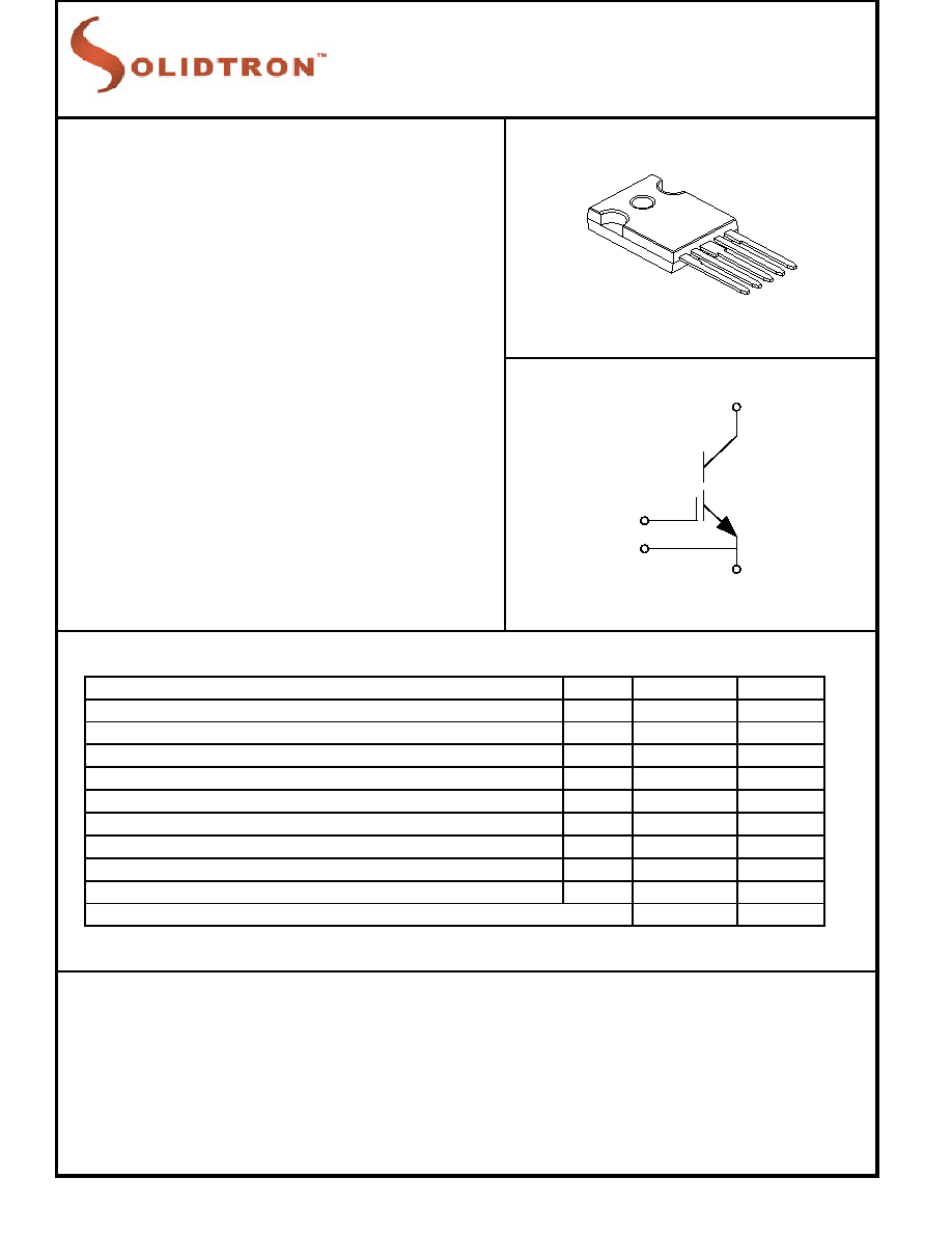
Package
Schematic Symbol
Features
Absolute Maximum Ratings
SYMBOL
VALUE
UNITS
Peak Off-State Voltage
V
DRM
1400
V
Peak Reverse Voltage
V
RRM
-5
V
Off-State Rate of Change of Voltage Immunity
dv/dt
5000
V/uSec
Continuous Anode Current at 110
o
C
I
A110
65
A
Repetitive Peak Anode Current (Pulse Width=1uSec)
I
ASM
6000
A
Rate of Change of Current
dI/dt
125
kA/uSec
Continuous Gate-Cathode Voltage
V
GKS
+/-20
V
Peak Gate-Cathode Voltage
V
GKM
+/-25
V
Minimum Negative Gate-Cathode Voltage Required for Garanteed Off-State
V
GK(OFF-MIN)
-5
V
Maximum Junction Temperature
T
JM
150
o
C
Maximum Soldering Temperature (Installation)
260
o
C
This SILICON POWER product is protected by one or more of the following U.S. Patents:
5,446,316
5,557,656
5,564,226
5,517,058
4,814,283
5,135,890
5,521,436
5,585,310
5,248,901
5,366,932
5,497,013
5,532,635
5,105,536
5,777,346
5,446,316
5,577,656
5,473,193
5,166,773
5,209,390
5,139,972
5,103,290
5,028,987
5,304,847
5,569,957
4,958,211
5,111,268
5,260,590
5,350,935
5,640,300
5,184,206
5,206,186
5,757,036
5,777,346
5,995,349
4,801,985
4,476,671
4,857,983
4,888,627
4,912,541
5,424,563
5,399,892
5,468,668
5,082,795
4,980,741
4,941,026
4,927,772
4,739,387
4,648,174
4,644,637
4,374,389
4,750,666
4,429,011
5,293,070
This voltage controlled Solidtron (VCS) discharge switch utilizes
an n-type MOS-Controlled Thyristor mounted in a five leaded TO-
247 plastic package.
The VCS features the high peak current capability and low On-
state voltage drop common to SCR thyristors combined with
extremely high dI/dt capability. This semiconductor is intended
for the control of high power circuits with the use of very small
amounts of input energy and is ideally suited for capacitor
discharge applications.
The industry standard TO-247 package allows for assembly of
the Solidtron using automated insertion equipment.
l
1400V Peak Off-State Voltage
l
65A Continuous Rating
l
6kA Surge Current Capability
l
>100kA/uSec dI/dt Capability
l
<150nSec Turn-On Delay
l
Low On-State Voltage
l
MOS Gated Control
l
Low Inductance Package
Anode (A)
Gate (G)
Cathode (K)
Gate Return (GR)
5 Lead TO-247
Advanced Pulse Power Device
N-MOS VCS, TO-247
SMCT AA65N14A10
1

Performance Characteristics
T
J
=25
o
C unless otherwise specified
Measurements
Parameters
Symbol
Test Conditions
Min.
Typ.
Max.
Units
Anode to Cathode Breakdown Voltage
V
(BR)
V
GK
=-5, I
A
=1mA
1400
V
Anode-Cathode Off-State Current
i
D
V
GE
=-5V, V
AK
=1200V
T
C
=25
o
C
<10
100
uA
T
C
=150
o
C
250
1000
uA
Gate-Cathode Turn-On Threshold Voltage
V
GK(TH)
V
AK
=V
GK
, I
AK
=1mA
0.7
V
Gate-Cathode Leakage Current
I
GK(lkg)
V
GK
=+/-20V
750
nA
Anode-Cathode On-State Voltage
V
T
I
T
=65A, V
GK
=+5V
T
C
=25
o
C
1.3
1.8
V
(See Figures 1,2 & 3)
T
C
=150
o
C
1.1
1.4
V
Input Capacitance
C
ISS
18
nF
Turn-on Delay Time
t
D(ON)
0.2uF Capacitor Discharge
82
150
nS
Rate of Change of Current
dI/dt
T
J
=25
o
C, V
GK
= -5V to +5V
58
kA/uSec
Peak Anode Current
I
P
V
AK
=800V, RG=4.7
3300
A
Discharge Event Energy
E
DIS
L
S
= 8nH (See Figures 4,5 & 6)
36
mJ
Turn-on Delay Time
t
D(ON)
0.2uF Capacitor Discharge
64
120
nS
Rate of Change of Current
dI/dt
T
J
=150
o
C, V
GK
= -5V to +5V
100
kA/uSec
Peak Anode Current
I
P
V
AK
=1200V, RG=4.7
5200
A
Discharge Event Energy
E
DIS
L
S
= 8nH (See Figures 4,5 & 6)
74
mJ
Junction to Case Thermal Resistance
R
JC
Anode (bottom) side cooled (Note 1.)
0.035
o
C/W
Typical Performance Curves
(unless otherwise specified)
Typical Performance Curves
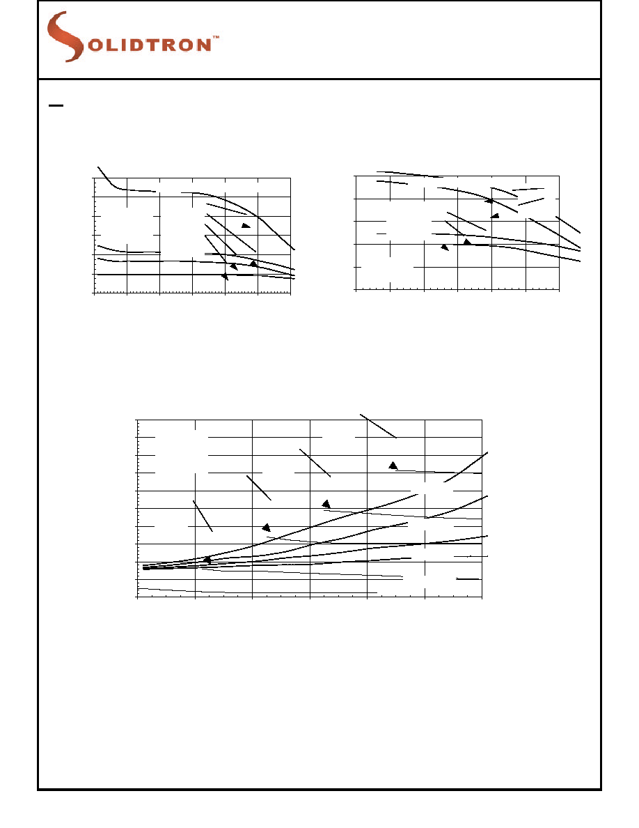
Figure 1. On-State Characteristics
Figure 2. On-State Characteristics
Figure 3. Predicted High Current On-State Characteristics
0
50
100
150
200
250
300
350
0.0
0.5
1.0
1.5
2.0
2.5
V
T
- On-State Voltage=Volts
I
T
- On-State Current-A
V
GK
=+5V
Pulse Duration = 250uSec.
Duty Cycle=<0.5%
T
J
=25
o
C
T
J
=150
o
C
0
10
20
30
40
50
60
70
80
0.0
0.2
0.4
0.6
0.8
1.0
1.2
1.4
V
T
- On-State Voltage=Volts
I
T
- On-State Current-A
V
GK
=+5V
Pulse Duration = 250uSec.
Duty Cycle=<0.5%
T
J
=25
o
C
T
J
=150
o
C
0
1000
2000
3000
4000
5000
6000
0
4
8
12
16
20
24
V
T
- On-State Voltage - V
I
T
- On-State Current-A
T
J
=25
o
C
R
ON
= 3.5m
T
J
=150
o
C
R
ON
= 3.9m
Advanced Pulse Power Device
N-MOS VCS, TO-247
SMCT AA65N14A10