SPT312
3000A, 4500V
100mm Thyristor
Features
Package
3000A, 4500V
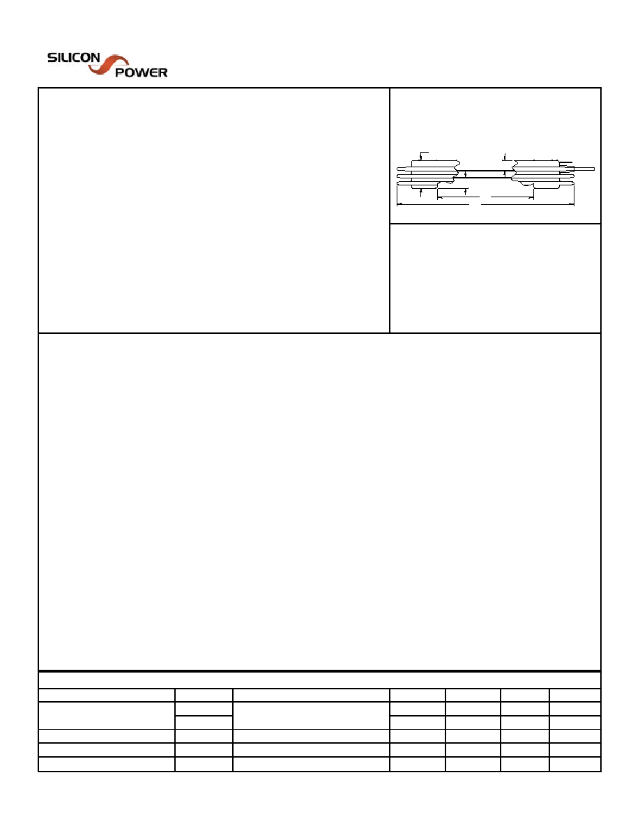
A=5.375in, B=3.204in, C=0.792in, D=0.2902in
40kA Pulse Current Capability
Notes - 1, 2 & 3
Fast Turn-off Time
Light Weight Package
Description
The SPT312 reverse blocking thyristor is suitable for inverter applications up to
200Hz. The silicon junction is manufactured by the proven multi-diffusion process
and utilizes the exclusive eight (8) arms involute gate structure for lower switching
losses.
MODEL RATING AVAILABILITY
The design utilizes the revolutionary "Light Silicon Sandwich" or LSS technology,
PART NUMBER
V
DRM
V
RRM
a new termination technique which eliminates heavy refractory metal as a
SPT312HK
4500
4500
substrate but still employs the alloyed anode interface necessary for high surge
SPT312HH
4400
4400
current duty. The light weight plastic package allows the insertion of liquid
SPT312HF
4300
4300
cooled chillers closer to the silicon junction. Copper inserts can be supplied for
SPT312HD
4200
4200
adjoining commercially available flat surfaced heat dissipators.
SPT312HB
4100
4100
SPT312FT
4000
4000
Limiting Characteristics and Ratings
At T
J
= 125
o
C, Unless Otherwise Specified
SYMBOL
UNITS
Repetitive Peak Off State Voltage........................................................................................................................
V
DRM
4500
V
Repetitive Peak Reverse Voltage.........................................................................................................................
V
RRM
4500
V
Average On-State Current (T
C
=70
o
C) ..............................................................................................................
I
T(AV)
3000
A
Peak Half-Cycle Non-Repetitive Surge Current ( 8.3ms / 10ms )..............................................................
I
TSM
40 / 37.5
kA
For Fusing ( 8.3ms / 10ms ) ......................................................................................
I
2
t
6.6 / 7
MA
2
s
Critical Gate Trigger Voltage ( V
D
= 12V, T
J
= 25
o
C )......................................................................................
V
GT
4.5
V
Critical Gate Trigger Current ( V
D
= 12V, T
J
= 25
o
C ) ........................................................................................
I
GT
300
mA
Non-Trigger Gate Voltage ( V
D
= 2000V ) ......................................................................................................................................
V
GD
0.8
V
Non-Trigger Gate Current ( V
D
= 2000V ) ......................................................................................................................................
I
GD
15
mA
Open Circuit Gate Voltage ........................................................................................................................................
V
OC
50
V
Short Circuit Gate Current .......................................................................................................................................
I
SS
5
A
Gate Pulse Duration and Rise Time .....................................................................................................................
10
�
s duration / 0.5
�
s rise time
Turn-Off Time (5A/
�
s, >100V, 400V/
�
s to 2000V) .............................................................................................................................................................................
Toff
400
�
s
Turn-On Delay (V
D
= 50%V
DRM
) ........................................................................................................................................................................................................
td
4
�
s
Rate of Change of Voltage ( V
D
=70% V
DRM
) .......................................................................................................
dv/dt
1000
V/
�
s
Rate of Change of Current ( V
D
=50% V
DRM
) .....................................................................................
di/dt
300
A/
�
s
Operating and Storage Temperature.....................................................................................................................
T
J
, T
STG
0 to +125
o
C
Mounting Force............................................................................................................................................................
F 13000-16000 lbs
Notes
1. Optional external posts dwg. # 0215B8331; Ni plated copper, 0.35" thick each.
2. Compressed thickness including external posts is 0.88" - 0.89" (22.35mm - 22.61mm).
3. Weight 14 oz., 2.7 lbs with posts.
Electrical Specifications
At T
J
= 125
o
C, Unless Otherwise Specified
PARAMETERS
SYMBOL TEST CONDITIONS
MIN
TYP
MAX
UNITS
Peak Off State Blocking
I
DRM
V
D
= 80%V
DRM
450
mA
Forward & Reverse Current
I
RRM
350
mA
On State Voltage
V
TM
I
T
= 4kA Pulse
2.0
V
Max. Peak Recovery Current
I
RM
di/dt = 10A/
�
s
Snap. S = .5-.33
310
A
Thermal Resistance
R
JC
Double Side Cooling
0.0049
o
C/W
C
D
D
B
A
175 Great Valley Pkwy. Malvern, PA 19355 USA
Spt312.xls Rev. 1 7/09/2001
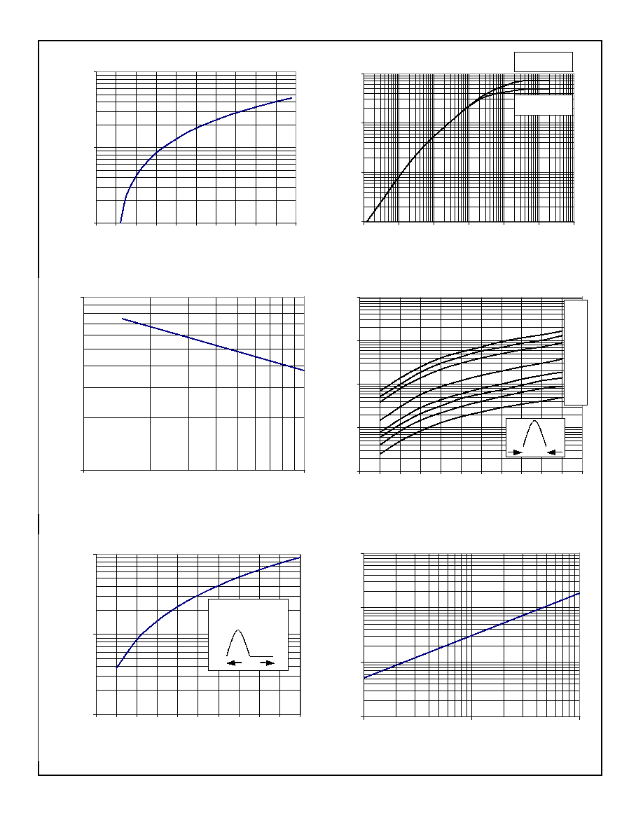
Typical Performance Curves
FIGURE 1. ON-STATE CURRENT vs ON-STATE VOLTAGE
FIGURE 2. THERMAL IMPEDANCE vs POWER ON TIME
FIGURE 3. PEAK I
TSM
vs PULSE DURATION FOR HALF SINE CURRENT
FIGURE 4. ON-STATE ENERGY vs ON-STATE CURRENT
FIGURE 5. AVERAGE FULL CYCLE POWER LOSS vs ON-STATE CURRENT
FIGURE 6. PEAK I
REC
vs COMMUTATING di/dt
100
1000
10000
0
1
2
3
4
5
6
7
8
9
10
Peak Current, It (kA)
Average Power (W)
0.1
1
10
100
1000
0
1
2
3
4
5
6
7
8
9
10
11
Peak Current, It (kA)
Energy per Pulse, (J)
1000
10000
100000
0
1
2
3
4
5
6
7
8
9
10
On-State Voltage, Vtm (V)
On-state Current, It (A)
10
100
1
10
Surge Duration (ms)
Peak Surge Current, Itsm (kA)
pulse
width
(us)
9000
7000
5000
2000
1000
750
500
250
tp
1/f
applicable frequency
range: 50 - 200Hz
0.00001
0.0001
0.001
0.01
0.0001
0.001
0.01
0.1
1
10
100
Power On-Time (sec)
Zthj- (
o
C/W)
with copper
inserts 0.0074
without copper
inserts 0.0049
10
100
1000
10000
1
10
100
Commutating di/dt (A/us)
Peak recovery current (A)
175 Great Valley Pkwy. Malvern, PA 19355 USA
Spt312.xls Rev. 1 7/09/2001