Type SPT315 thyristor is optimized especially for pulse power and static transfer switch applications
for which lowest on-state voltage is achieved. The silicon junction design utilizes a second generation
pilot gate and a unique orientation of emitter shorts which promote the lateral expansion of conducting
plasma resulting in lower spreading losses while achieving high dv/dt withstand. It is supplied in a
reliable plastic light weight package. The design utilizes a new termination technique which
eliminates heavy refractory metal as a substrate but still employs the alloyed anode interface necessary
for high surge current duty. External posts are available for adjoining commercially available heat
dissipators using clamping hardware.
175 GREAT VALLEY PKWY. MALVERN, PA 19355
U S A
ON-STATE CHARACTERISTIC
Process Maximum
1000
10000
0
1
2
3
4
5
6
7
On-State Current, It (A)
On-State Voltage, Vt (V)
On-State Voltage, Vt (V)
01A
Process Maximum
Pulsed Current
Tcase = 125 C
60000
Maximum Off-State & Reverse
Blocking Voltage Ratings
97f:pm5
T
J
= 0 to 115
o
C
V
DRM
V
RRM
(volts)
SPT315DK
2500
2500
SPT315DH
2400
2400
SPT315DF
2300
2300
SPT315DD
2200
2200
SPT315DB
2100
2100
SPT315TT
2000
2000
External clamping force
15000 - 18000 lb
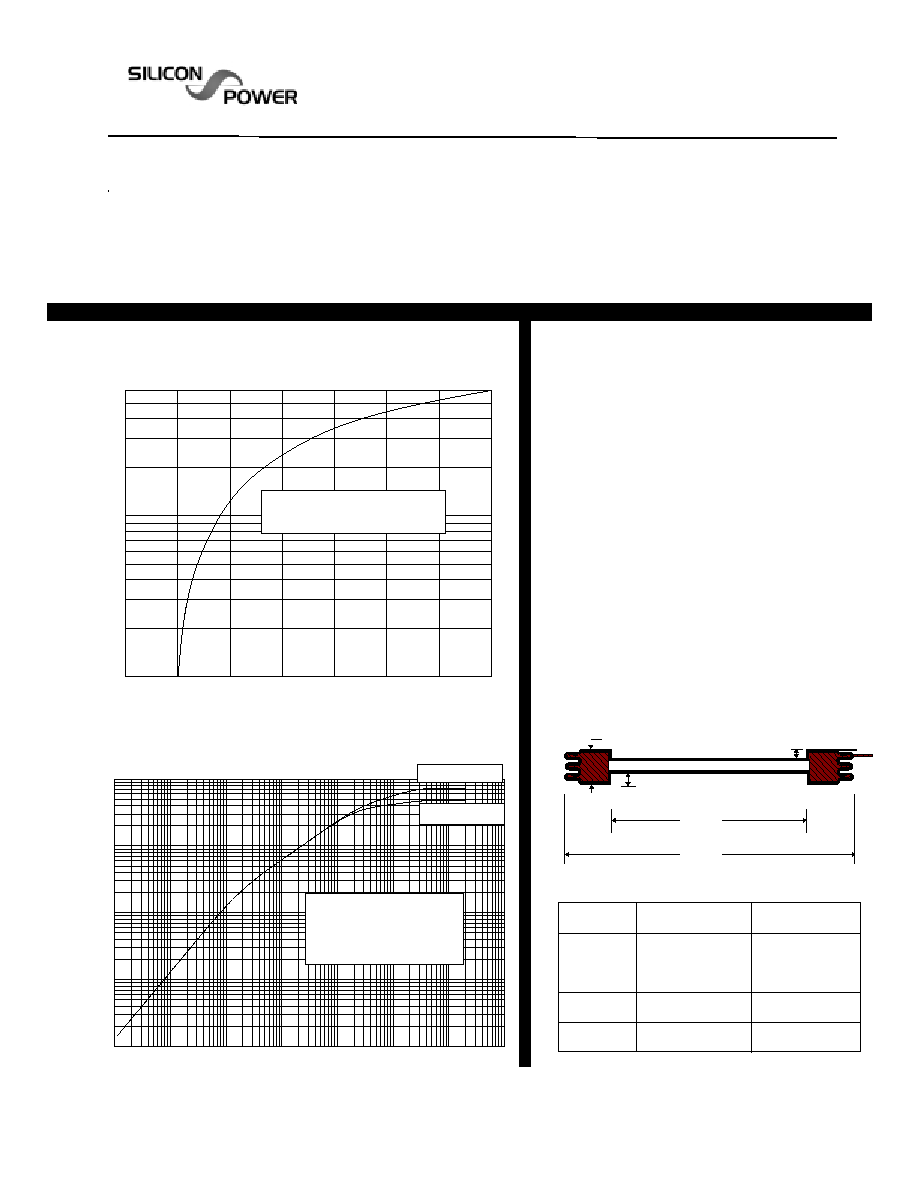
Optional external posts drw.# 0215B8331
Ni plated copper, 0.350" thick each.
Compressed thickness including external posts
0.885 "
Weight: 10 oz
2 lb 9 oz with posts
1.000E-06
1.000E-05
1.000E-04
1.000E-03
0.01
THERMAL IMPEDANCE vs. ON-TIME
Zthj_(degC/watt)
to sink* .0073
through external copper
post inserts
* double sided cooling
to case .0049
Power On-Time (seconds)
100
10
1
0.1
.01
.001
.0001
SPT315 100mm
SPT315 100mm
SPT315 100mm
SPT315 100mm
SPT315 100mm THYRIST
THYRIST
THYRIST
THYRIST
THYRISTO R
O R
O R
O R
O R
2500V / 4700A
2500V / 4700A
2500V / 4700A
2500V / 4700A
2500V / 4700A
02/15/01
D
D
B
A
Nominal Dimensions
A
B
C
D
inch
mm
5
136.5
85
20.24
0.306
7.77
3/8
51/64
3
dia.
dia.
dia.
dia.
C
11/32
SPT315
Repetitive peak off-
Repetitive peak off-
Repetitive peak off-
Repetitive peak off-
Repetitive peak off-
V
V
V
V
V
D R M
D R M
D R M
D R M
D R M
T
T
T
T
T
J
J
J
J
J
=0
=0
=0
=0
=0
up to
up to
up to
up to
up to
V
V
V
V
V
state & reverse volts
state & reverse volts
state & reverse volts
state & reverse volts
state & reverse volts
V
V
V
V
V
R R M
R R M
R R M
R R M
R R M
to 115
to 115
to 115
to 115
to 115
o
o
o
o
o
C
C
C
C
C
2600
2600
2600
2600
2600
Repetitive peak off-
Repetitive peak off-
Repetitive peak off-
Repetitive peak off-
Repetitive peak off-
I
I
I
I
I
D R M
D R M
D R M
D R M
D R M
T
T
T
T
T
J
J
J
J
J
=0
=0
=0
=0
=0
300
300
300
300
300
m a
m a
m a
m a
m a
state & reverse current
state & reverse current
state & reverse current
state & reverse current
state & reverse current I
I
I
I
I
R R M
R R M
R R M
R R M
R R M
to 115
to 115
to 115
to 115
to 115
o
o
o
o
o
C
C
C
C
C
300
300
300
300
300
Average on-state
Average on-state
Average on-state
Average on-state
Average on-state
I
I
I
I
I
T(AV)
T(AV)
T(AV)
T(AV)
T(AV)
T
T
T
T
T
case
case
case
case
case
=
=
=
=
=
4700
4700
4700
4700
4700
A
A
A
A
A
current
current
current
current
current
70
70
70
70
70
o
o
o
o
o
C
C
C
C
C
Peak half-cycle
Peak half-cycle
Peak half-cycle
Peak half-cycle
Peak half-cycle
I
I
I
I
I
T S M
T S M
T S M
T S M
T S M
8.3 ms
8.3 ms
8.3 ms
8.3 ms
8.3 ms
60
60
60
60
60
kA
kA
kA
kA
kA
non-rep surge current
non-rep surge current
non-rep surge current
non-rep surge current
non-rep surge current
1.5 ms
1.5 ms
1.5 ms
1.5 ms
1.5 ms
90
90
90
90
90
T
T
T
T
T
J
J
J
J
J
=115
=115
=115
=115
=115
o
o
o
o
o
C
C
C
C
C
On-state voltage
On-state voltage
On-state voltage
On-state voltage
On-state voltage
V
V
V
V
V
T M
T M
T M
T M
T M
I
I
I
I
I
T
T
T
T
T
=4000A
=4000A
=4000A
=4000A
=4000A
1.3
1.3
1.3
1.3
1.3
V
V
V
V
V
T
T
T
T
T
J
J
J
J
J
=115
=115
=115
=115
=115
o
o
o
o
o
C
C
C
C
C
Critical gate trigger
Critical gate trigger
Critical gate trigger
Critical gate trigger
Critical gate trigger
I
I
I
I
I
G T
G T
G T
G T
G T
V
V
V
V
V
D
D
D
D
D
= 12 V
= 12 V
= 12 V
= 12 V
= 12 V
200
200
200
200
200
m a
m a
m a
m a
m a
current / voltage
current / voltage
current / voltage
current / voltage
current / voltage
V
V
V
V
V
G T
G T
G T
G T
G T
T
T
T
T
T
J
J
J
J
J
= 25
= 25
= 25
= 25
= 25
o
o
o
o
o
C
C
C
C
C
5
5
5
5
5
V
V
V
V
V
Non-trigger gate
Non-trigger gate
Non-trigger gate
Non-trigger gate
Non-trigger gate
I
I
I
I
I
G D
G D
G D
G D
G D
V
V
V
V
V
D
D
D
D
D
= 2000V
= 2000V
= 2000V
= 2000V
= 2000V
15
15
15
15
15
m a
m a
m a
m a
m a
current
current
current
current
current
T
T
T
T
T
J
J
J
J
J
= 90
= 90
= 90
= 90
= 90
o
o
o
o
o
C
C
C
C
C
Maximum peak
Maximum peak
Maximum peak
Maximum peak
Maximum peak
I
I
I
I
I
R M
R M
R M
R M
R M
di/dt = 2 A/us
di/dt = 2 A/us
di/dt = 2 A/us
di/dt = 2 A/us
di/dt = 2 A/us
117
117
117
117
117
A
A
A
A
A
recovery current
recovery current
recovery current
recovery current
recovery current
T
T
T
T
T
J
J
J
J
J
= 115
= 115
= 115
= 115
= 115
o
o
o
o
o
C
C
C
C
C
snappiness F = 2-3
snappiness F = 2-3
snappiness F = 2-3
snappiness F = 2-3
snappiness F = 2-3
Critical rate of rise
Critical rate of rise
Critical rate of rise
Critical rate of rise
Critical rate of rise
di/dt
di/dt
di/dt
di/dt
di/dt
T
T
T
T
T
J
J
J
J
J
=115
=115
=115
=115
=115
o
o
o
o
o
C
C
C
C
C
100
100
100
100
100
A/us
A/us
A/us
A/us
A/us
of on-state current
of on-state current
of on-state current
of on-state current
of on-state current
rep
rep
rep
rep
rep
60 Hz
60 Hz
60 Hz
60 Hz
60 Hz
with 60A snubber discharge
with 60A snubber discharge
with 60A snubber discharge
with 60A snubber discharge
with 60A snubber discharge
Critical rate of rise
Critical rate of rise
Critical rate of rise
Critical rate of rise
Critical rate of rise
dv/dt
dv/dt
dv/dt
dv/dt
dv/dt
T
T
T
T
T
J
J
J
J
J
=90
=90
=90
=90
=90
o
o
o
o
o
C
C
C
C
C
1000
1000
1000
1000
1000
V/us
V/us
V/us
V/us
V/us
of off-state voltage
of off-state voltage
of off-state voltage
of off-state voltage
of off-state voltage
V
V
V
V
V
D
D
D
D
D
= 67% V
= 67% V
= 67% V
= 67% V
= 67% V
D R M
D R M
D R M
D R M
D R M
Turn-on delay
Turn-on delay
Turn-on delay
Turn-on delay
Turn-on delay
t
t
t
t
t
d
d
d
d
d
V
V
V
V
V
D
D
D
D
D
= 50%V
= 50%V
= 50%V
= 50%V
= 50%V
D R M
D R M
D R M
D R M
D R M
3
3
3
3
3
us
us
us
us
us
T
T
T
T
T
J
J
J
J
J
=115
=115
=115
=115
=115
o
o
o
o
o
C
C
C
C
C
Turn-off time
Turn-off time
Turn-off time
Turn-off time
Turn-off time
T
T
T
T
T
off
off
off
off
off
5A/us,-100V
5A/us,-100V
5A/us,-100V
5A/us,-100V
5A/us,-100V
300
300
300
300
300
us
us
us
us
us
20V/us to 2000V
20V/us to 2000V
20V/us to 2000V
20V/us to 2000V
20V/us to 2000V
10
100
1000
1
10
100
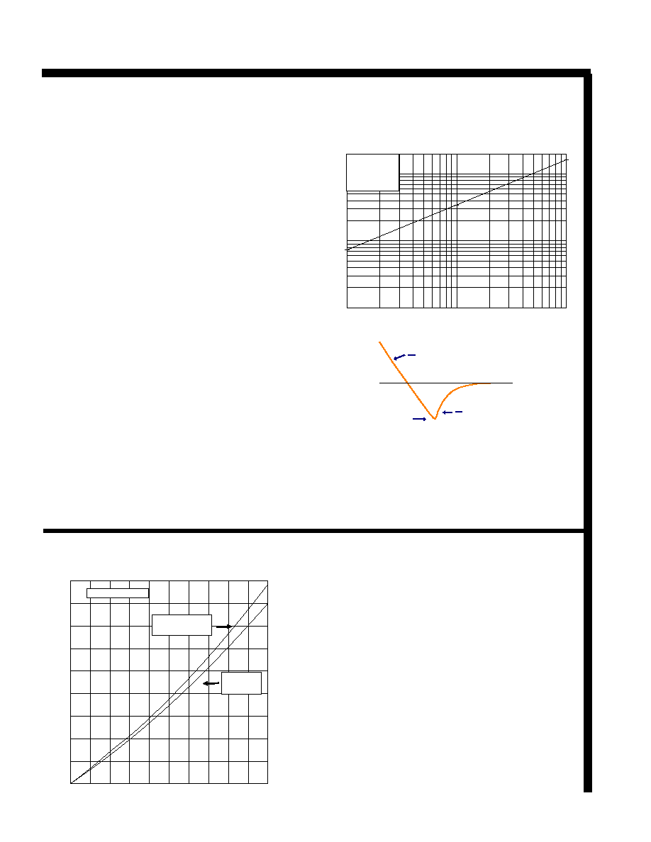
Peak Recovery Current Relationship
with Commutating di/dt
Peak Recovery Current, Irm, (A)
Commutating di/dt, (A/us)
Commutating di/dt, (A/us)
2000
Process Limit
Itm = 100 kA
Tj = 115 C
di
dt
di
dt
RM
(REC)
t
Snappiness
F = di/dt(rec) / di/dt
I
Recommended gate drive to sustain turn-on di/dt rating
V
OC
= 40 V
I
SS
= 4 A
rise time = 0.5 us
duration 10 - 20 us
0
250
500
750
1000
1250
1500
1750
2000
2250
0
0.5
1
1.5
2
2.5
3
3.5
4
4.5
5
FULL CYCLE AVERAGE POWER LOSS
versus
PEAK CURRENT at 50/60 Hz
Peak Current, It (kA)
Peak Current, It (kA)
01A
(plasma spreading and conduction loss)
overlap angle
= 20 degree
180 degree
sinewave
120 deg.sq. wave
Tj = 115 degC
FULL CYCLE AVERAGE POWER LOSS
50 / 60 Hz T
J
= 115
o
C
I
T
(peak)
half-sine
3ph
180
o
120
o
amperes
watts
watts
500
153
162
1000
316
336
1500
489
524
2000
673
725
2500
868
939
3000
1073
1167
3500
1289
1408
4000
1516
1663
4500
1753
1930
5000
2000
2212
o1A: 2/15/01