
175 GREAT VALLEY PKWY. MALVERN, PA 19355
U S A
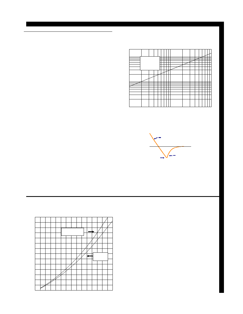
ON-STATE CHARACTERISTIC
Process Maximum
1000
10000
0
1
2
3
4
5
6
7
8
9
10
11
12
13
On-State Current, It (A)
On-State Voltage, Vt (volts)
On-State Voltage, Vt (volts)
96d:t401onst
70000
Process Maximum
Tcase = 115 C
8.3 ms pulses
Maximum Off-State & Reverse
Blocking Voltage Ratings
97c:pm5
T
J
= 0 to 115
o
C
V
DRM
V
RRM
(volts)
SPT401HT
5000
5000
SPT401HS
4900
4900
SPT401HR
4800
4800
SPT401HP
4700
4700
SPT401HM
4600
4600
SPT401HK
4500
4500
External clamping force
25000 lb minimum
Optional external posts drw.# 0215B8315
Ni plated copper, 0.35" thick each.
Compressed thickness including external posts
0.89" - 0.90"
Weight: 18 oz
3 lb 10 oz with posts
1.000E-07
1.000E-06
1.000E-05
1.000E-04
1.000E-03
0.01
THERMAL IMPEDANCE vs. ON-TIME
Zthj-c (deg C/W)
Power On-Time (seconds)
Power On-Time (seconds)
7/1/97 rev 96d:
.0001
.001
.01
.1
1.
10
.0031
.0047
to sink*
to case
* double sided cooling
through external copper
post inserts
Rev 5 2/10/2000
SPT401 125mm
SPT401 125mm
SPT401 125mm
SPT401 125mm
SPT401 125mm THYRIST
THYRIST
THYRIST
THYRIST
THYRISTO R
O R
O R
O R
O R
5000V 5000A
5000V 5000A
5000V 5000A
5000V 5000A
5000V 5000A
Type SPT401 thyristor is suitable for phase control applications such as for HVDC valves, static VAR compensators
and synchronous motor drives. A second generation pilot gate and a unique orientation of emitter shorts are emoloyed
which promote the lateral expansion of conducting plasma resulting in lower spreading losses and high dv/dt
withstand. It is supplied in a reliable plastic light weight package
reliable plastic light weight package
reliable plastic light weight package
reliable plastic light weight package
reliable plastic light weight package. The design utilizes SPCO's revolutionary
"Lightweight Silicon Sandwich", LSS
LSS
LSS
LSS
LSS technology, a new termination technique which eliminates heavy refractory
metal as a substrate while retaining an alloyed anode interface necessary for high surge current duty. External posts
are available for adjoining commercially available heat dissipators using clamping hardware.
C
D
D
B
A
Nominal Dimensions
A
B
C
D
inch
mm
6
162.7
106.4
20.24
7.52
13/32
3/16
51/64
4
dia.
dia.
dia.
dia.
C
0.2961
SPT401
SPT401
SPT401
SPT401
SPT401
10
100
1000
1
10
100
Peak Recovery Current Relationship
with Commutating di/dt
Peak Recovery Current, Irm, (A)
Commutating di/dt, (A/us)
Commutating di/dt, (A/us)
2000
Process Limit
Itm = 100 kA
Tj = 115 C
LIMITING CHARACTERISTICS AND RATINGS
LIMITING CHARACTERISTICS AND RATINGS
LIMITING CHARACTERISTICS AND RATINGS
LIMITING CHARACTERISTICS AND RATINGS
LIMITING CHARACTERISTICS AND RATINGS
0
1
2
3
4
5
6
7
8
9
10
11
12
13
14
0
1
2
3
4
5
6
7
8
9
10 11 12 13 14 15
FULL CYCLE AVERAGE POWER LOSS
versus
PEAK CURRENT at 50/60 Hz
Pavg (kilowatts)
Peak Current, It (kA)
Peak Current, It (kA)
96d:
(plasma spreading and conduction loss)
overlap angle
= 20 degree
180 degree
sinewave
120 deg.sq. wave
Tj = 115 degC
97c: Rev. 5 2/10/2000
1000
359
414
2000
900
1013
3000
1511
1689
4000
2179
2432
5000
2900
3242
6000
3676
4119
7000
4506
5068
8000
5393
6090
9000
6339
7188
10000
7345
8365
11000
8414
9623
12000
9545
10964
13000
10742
12390
14000
12005
13902
15000
13335
15503
I
T
(peak)
half-sine
3ph
180
o
120
o
amperes
watts
watts
FULL CYCLE AVERAGE POWER LOSS
50 / 60 Hz T
J
= 115
o
C
Recommended gate drive to sustain turn-on di/dt rating
V
OC
= 50 V
I
SS
= 5 A
rise time = 0.5 us
duration 10 - 20 us
di
dt
di
dt
RM
(REC)
t
Snappiness
F = di/dt(rec) / di/dt
I
Repetitive peak off-
Repetitive peak off-
Repetitive peak off-
Repetitive peak off-
Repetitive peak off-
V
V
V
V
V
D R M
D R M
D R M
D R M
D R M
T
T
T
T
T
J
J
J
J
J
=0
=0
=0
=0
=0
up to
up to
up to
up to
up to
V
V
V
V
V
state & reverse volts
state & reverse volts
state & reverse volts
state & reverse volts
state & reverse volts
V
V
V
V
V
R R M
R R M
R R M
R R M
R R M
to 115
to 115
to 115
to 115
to 115
o
o
o
o
o
C
C
C
C
C
5000
5000
5000
5000
5000
Repetitive working
Repetitive working
Repetitive working
Repetitive working
Repetitive working
V
V
V
V
V
D W M
D W M
D W M
D W M
D W M
T
T
T
T
T
J
J
J
J
J
=0
=0
=0
=0
=0
0.8V
0.8V
0.8V
0.8V
0.8V
D R M
D R M
D R M
D R M
D R M
V
V
V
V
V
crest voltage
crest voltage
crest voltage
crest voltage
crest voltage
V
V
V
V
V
R W M
R W M
R W M
R W M
R W M
to 115
to 115
to 115
to 115
to 115
o
o
o
o
o
C
C
C
C
C
0.8V
0.8V
0.8V
0.8V
0.8V
R R M
R R M
R R M
R R M
R R M
Peak off-state
Peak off-state
Peak off-state
Peak off-state
Peak off-state
I
I
I
I
I
D W M
D W M
D W M
D W M
D W M
T
T
T
T
T
J
J
J
J
J
=0
=0
=0
=0
=0
250
250
250
250
250
m a
m a
m a
m a
m a
& reverse current
& reverse current
& reverse current
& reverse current
& reverse current
I
I
I
I
I
R W M
R W M
R W M
R W M
R W M
to 115
to 115
to 115
to 115
to 115
o
o
o
o
o
C
C
C
C
C
100
100
100
100
100
Average on-state
Average on-state
Average on-state
Average on-state
Average on-state
I
I
I
I
I
T(AV)
T(AV)
T(AV)
T(AV)
T(AV)
T
T
T
T
T
case
case
case
case
case
=
=
=
=
=
5000
5000
5000
5000
5000
A
A
A
A
A
current
current
current
current
current
70
70
70
70
70
o
o
o
o
o
C
C
C
C
C
Peak half-cycle
Peak half-cycle
Peak half-cycle
Peak half-cycle
Peak half-cycle
I
I
I
I
I
T S M
T S M
T S M
T S M
T S M
8.3 ms
8.3 ms
8.3 ms
8.3 ms
8.3 ms
70
70
70
70
70
kA
kA
kA
kA
kA
non-rep surge current
non-rep surge current
non-rep surge current
non-rep surge current
non-rep surge current
1.5 ms
1.5 ms
1.5 ms
1.5 ms
1.5 ms
105
105
105
105
105
T
T
T
T
T
J
J
J
J
J
=115
=115
=115
=115
=115
o
o
o
o
o
C
C
C
C
C
On-state voltage
On-state voltage
On-state voltage
On-state voltage
On-state voltage
V
V
V
V
V
T M
T M
T M
T M
T M
I
I
I
I
I
T
T
T
T
T
=4000A
=4000A
=4000A
=4000A
=4000A
1.80
1.80
1.80
1.80
1.80
V
V
V
V
V
t
t
t
t
t
P
P
P
P
P
=8.3ms
=8.3ms
=8.3ms
=8.3ms
=8.3ms
T
T
T
T
T
J
J
J
J
J
=115
=115
=115
=115
=115
o
o
o
o
o
C
C
C
C
C
Critical gate trigger
Critical gate trigger
Critical gate trigger
Critical gate trigger
Critical gate trigger
I
I
I
I
I
G T
G T
G T
G T
G T
V
V
V
V
V
D
D
D
D
D
= 12 V
= 12 V
= 12 V
= 12 V
= 12 V
150
150
150
150
150
m a
m a
m a
m a
m a
current / voltage
current / voltage
current / voltage
current / voltage
current / voltage
V
V
V
V
V
G T
G T
G T
G T
G T
T
T
T
T
T
J
J
J
J
J
= 25
= 25
= 25
= 25
= 25
o
o
o
o
o
C
C
C
C
C
5.0
5.0
5.0
5.0
5.0
V
V
V
V
V
Non-trigger gate
Non-trigger gate
Non-trigger gate
Non-trigger gate
Non-trigger gate
I
I
I
I
I
G D
G D
G D
G D
G D
V
V
V
V
V
D
D
D
D
D
= 2000V
= 2000V
= 2000V
= 2000V
= 2000V
15
15
15
15
15
m a
m a
m a
m a
m a
current
current
current
current
current
V
V
V
V
V
G D
G D
G D
G D
G D
T
T
T
T
T
J
J
J
J
J
= 115
= 115
= 115
= 115
= 115
o
o
o
o
o
C
C
C
C
C
0.8
0.8
0.8
0.8
0.8
V
V
V
V
V
Maximum peak
Maximum peak
Maximum peak
Maximum peak
Maximum peak
I
I
I
I
I
R M
R M
R M
R M
R M
di/dt = 2 A/us
di/dt = 2 A/us
di/dt = 2 A/us
di/dt = 2 A/us
di/dt = 2 A/us
110
110
110
110
110
A
A
A
A
A
recovery current
recovery current
recovery current
recovery current
recovery current
T
T
T
T
T
J
J
J
J
J
= 115
= 115
= 115
= 115
= 115
o
o
o
o
o
C
C
C
C
C
snappiness F = 2-3
snappiness F = 2-3
snappiness F = 2-3
snappiness F = 2-3
snappiness F = 2-3
Critical rate of rise
Critical rate of rise
Critical rate of rise
Critical rate of rise
Critical rate of rise
di/dt
di/dt
di/dt
di/dt
di/dt
T
T
T
T
T
J
J
J
J
J
=115
=115
=115
=115
=115
o
o
o
o
o
C
C
C
C
C
100
100
100
100
100
A/us
A/us
A/us
A/us
A/us
of on-state current
of on-state current
of on-state current
of on-state current
of on-state current
rep
rep
rep
rep
rep
60 Hz
60 Hz
60 Hz
60 Hz
60 Hz
with 60A snubber discharge
with 60A snubber discharge
with 60A snubber discharge
with 60A snubber discharge
with 60A snubber discharge
Critical rate of rise
Critical rate of rise
Critical rate of rise
Critical rate of rise
Critical rate of rise
dv/dt
dv/dt
dv/dt
dv/dt
dv/dt
T
T
T
T
T
J
J
J
J
J
=115
=115
=115
=115
=115
o
o
o
o
o
C
C
C
C
C
1000
1000
1000
1000
1000
V/us
V/us
V/us
V/us
V/us
of off-state voltage
of off-state voltage
of off-state voltage
of off-state voltage
of off-state voltage
V
V
V
V
V
D
D
D
D
D
= 67% V
= 67% V
= 67% V
= 67% V
= 67% V
D R M
D R M
D R M
D R M
D R M
Turn-on delay
Turn-on delay
Turn-on delay
Turn-on delay
Turn-on delay
t
t
t
t
t
d
d
d
d
d
V
V
V
V
V
D
D
D
D
D
= 50%V
= 50%V
= 50%V
= 50%V
= 50%V
D R M
D R M
D R M
D R M
D R M
4
4
4
4
4
us
us
us
us
us
T
T
T
T
T
J
J
J
J
J
=115
=115
=115
=115
=115
o
o
o
o
o
C
C
C
C
C
Turn-off time
Turn-off time
Turn-off time
Turn-off time
Turn-off time
T
T
T
T
T
off
off
off
off
off
5A/us,-100V
5A/us,-100V
5A/us,-100V
5A/us,-100V
5A/us,-100V
400
400
400
400
400
us
us
us
us
us
20V/us to 2000V
20V/us to 2000V
20V/us to 2000V
20V/us to 2000V
20V/us to 2000V