SPT411A
4600A, 5000V
125mm Thyristor
Features
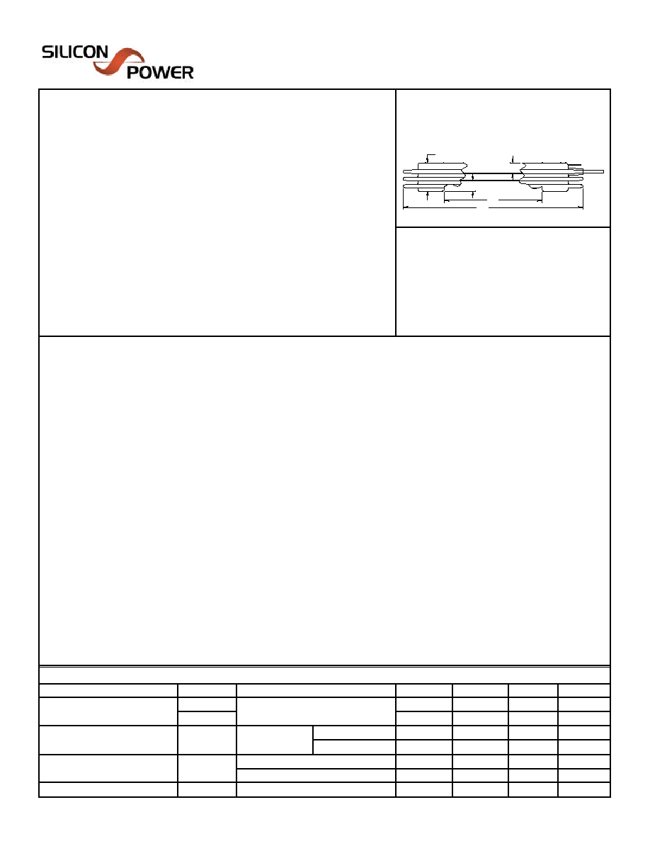
Package
4600A, 5000V
A=162.7mm, B=106.4mm, C=20.12mm, D=7.71mm
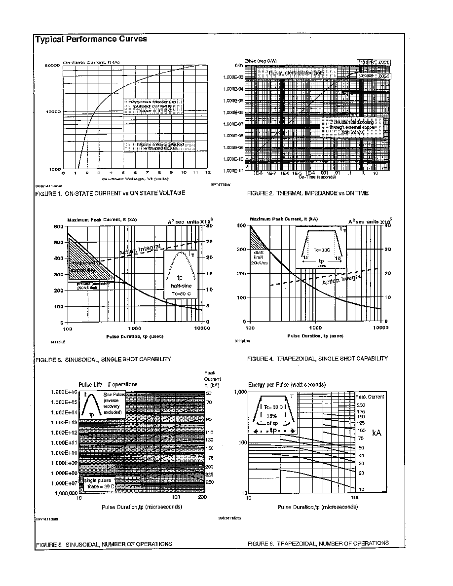
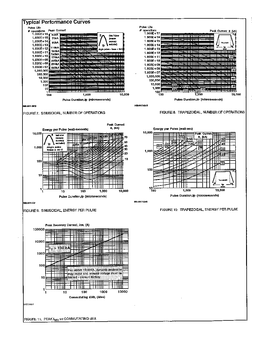
270kA Pulse Current Capability
Notes - 1, 2 & 3
20kA/
µ
S di/dt Pulse Capability
Low Power Gate Driver
Description
The SPT411A thyristor is optimized for pulse power applications. It features a
highly intedigitated cathode / pilot gate combinations which enable extremely
high pulse power di/dt driven with low gate power.
The design utilizes a revolutionary "Light Silicon Sandwich" or LSS technology,
MODEL RATING AVAILABILITY
a new termination technique which eliminates heavy refractory metal as a
PART NUMBER
V
DRM
V
RRM
substrate but still employs the alloyed anode interface necessary for high surge
SPT411AHT
5000
5000
current duty. This light weight plastic package allows the insertion of liquid
SPT411AHS
4900
4900
cooled chillers. Copper inserts can be supplied for adjoining commercially
SPT411AHR
4800
4800
available flat surfaced heat dissipators.
SPT411AHP
4700
4700
SPT411AHM
4600
4600
Limiting Characteristics and Ratings
At T
J
= 115
o
C, Unless Otherwise Specified
SYMBOL
UNITS
Repetitive Peak Off State Voltage........................................................................................................................
V
DRM
5000
V
Repetitive Peak Reverse Voltage.........................................................................................................................
V
RRM
5000
V
Average On-State Current (T
C
=70
o
C) ..............................................................................................................
I
T(AV)
4600
A
Peak Half-Cycle Non-Repetitive Surge Current ( 8.3ms / 1.5ms )..............................................................
I
TSM
77.5 / 143
kA
Critical Gate Trigger Voltage ( V
D
= 12V, T
J
= 25
o
C )......................................................................................
V
GT
5
V
Critical Gate Trigger Current ( V
D
= 12V, T
J
= 25
o
C ) ........................................................................................
I
GT
150
mA
Non-Trigger Gate Current ( V
D
= 2000V ) ......................................................................................................................................
I
GD
15
mA
Non-Trigger Gate Voltage ( V
D
= 2000V ) ......................................................................................................................................
V
GD
0.8
V
Open Circuit Gate Voltage ........................................................................................................................................
V
OC
100
V
Short Circuit Gate Current .......................................................................................................................................
I
SS
20
A
Gate Pulse Duration and Rise Time .....................................................................................................................
10
µ
s duration / 0.1
µ
s rise time
Turn-Off Time (5A/
µ
s, -100V, 20V/
µ
s to 2000V) .............................................................................................................................................................................
Toff
400
µ
s
Turn-On Delay (V
D
= 50%V
DRM
, T
J
=115
o
C) .......................................................................................................................................................................
td
4
µ
s
Rate of Change of Voltage ( V
D
=70% V
DRM
) .......................................................................................................
dv/dt
1000
V/
µ
s
Rate of Change of Current ( V
D
=50% V
DRM
, single shot capability
) ................................................................
di/dt
20
kA/
µ
s
Operating and Storage Temperature.....................................................................................................................
T
J
, T
STG
0 to +115
o
C
Mounting Force............................................................................................................................................................
F 25000-30000 lbs
Notes
1. Optional external posts dwg. # 0215B8315; Ni plated copper, 0.35" thick each.
2. Compressed thickness including external post is 0.88" - 0.89" (22.35mm - 22.61mm).
3. Weigh 18 oz., 3.6 lbs with posts.
Electrical Specifications
At T
J
= 115
o
C, Unless Otherwise Specified
PARAMETERS
SYMBOL TEST CONDITIONS
MIN
TYP
MAX
UNITS
Peak Off State Blocking
I
DRM
V
D
= 80%V
DRM
450
mA
Forward & Reverse Current
I
RRM
100
mA
On State Voltage
V
TM
I
T
= 10kA Pulse T
C
= +30
o
C
2
V
T
C
= +115
o
C
2.46
V
Max. Peak Recovery Current
I
RM
di/dt = 2A/
µ
s
Snap. S = .5-.33
110
A
di/dt = 2000A/
µ
s Snap. S = .5-.33
10000
A
Thermal Resistance
R
JC
Double Side Cooling
0.0034
o
C/W
C
D
D
B
A
175 Great Valley Pkwy. Malvern, PA 19355 USA
SPT411A-2.xls Rev. 5 7/9/2001