September 2003
1
Document Control # ML0002 rev 0.1
STK10C48
2K x 8 nvSRAM
QuantumTrapTM CMOS
Nonvolatile Static RAM
FEATURES
∑ 25ns, 35ns and 45ns Access Times
∑ STORE to Nonvolatile Elements Initiated by
Hardware
∑ RECALL to SRAM Initiated by Hardware or
Power Restore
∑ Automatic STORE Timing
∑ 10mA Typical I
CC
at 200ns Cycle Time
∑ Unlimited READ, WRITE and RECALL Cycles
∑ 1,000,000 STORE Cycles to Nonvolatile Ele-
ments
∑ 100-Year Data Retention over Full Industrial
Temperature Range
∑ Commercial and Industrial Temperatures
∑ 28-Pin 300 mil PDIP, 300 mil SOIC and
350 mil SOIC Packages
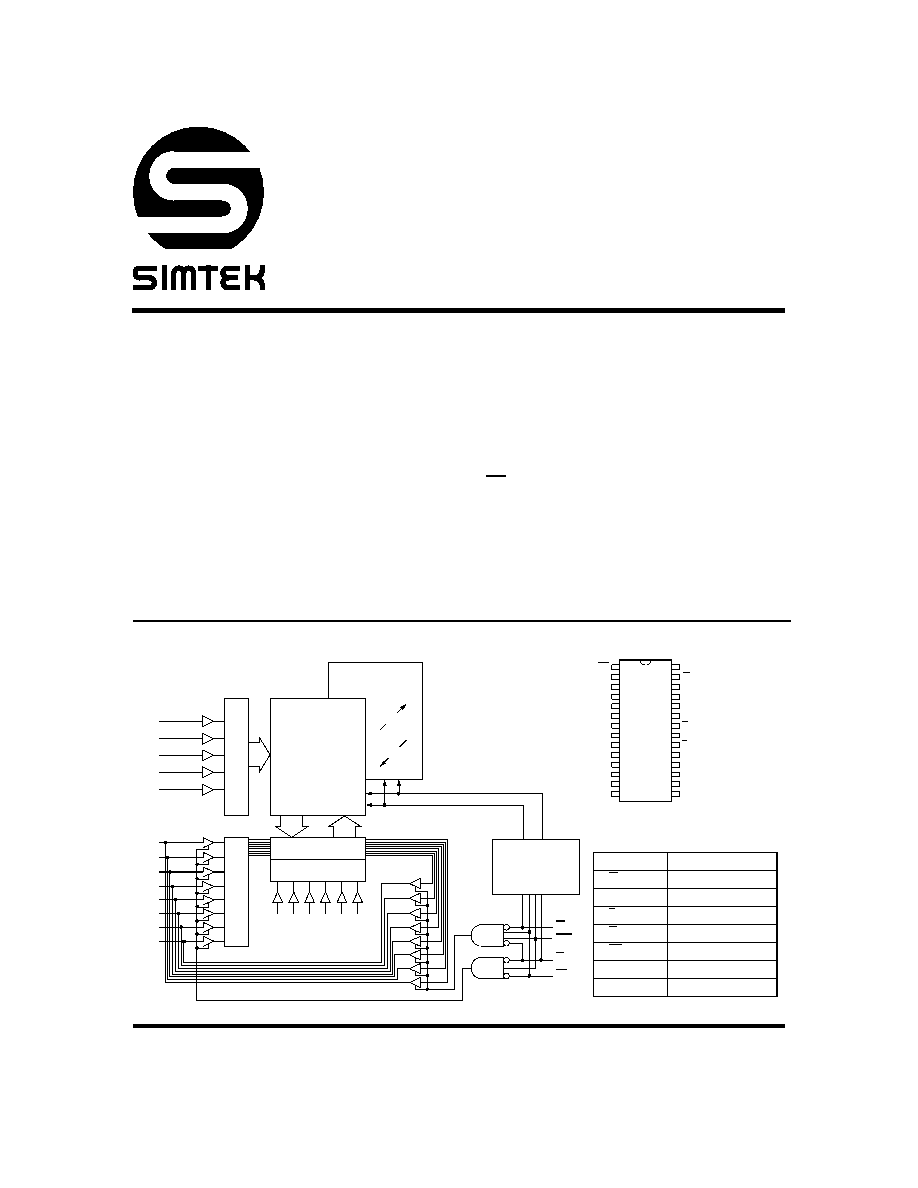
DESCRIPTION
The Simtek STK10C48 is a fast static
RAM
with a non-
volatile element incorporated in each static memory
cell. The
SRAM
can be read and written an unlimited
number of times, while independent nonvolatile data
resides in
t
he Nonvolatile Elements. Data may easily
be transferred from the
SRAM
to the Nonvolatile Ele-
ments (the
STORE
operation), or from the Nonvolatile
Elements to the
SRAM
(the
RECALL
operation), using
the NE pin. Transfers from the Nonvolatile Elements to
the
SRAM
(the
RECALL
operation) also take place auto-
matically on restoration of power. The STK10C48
combines the high performance and ease of use of a
fast
SRAM
with nonvolatile data integrity.
The STK10C48 features industry-standard pinout for
nonvolatile
RAM
s.
BLOCK DIAGRAM
COLUMN I/O
COLUMN DEC
STATIC RAM
ARRAY
32 x 512
ROW DECO
DER
IN
P
U
T BU
F
F
ER
S
Quantum Trap
32 x 512
STORE/
RECALL
CONTROL
STORE
RECALL
A
7
A
8
DQ
0
DQ
1
DQ
2
DQ
3
DQ
4
DQ
5
DQ
6
DQ
7
G
E
W
A
6
A
5
A
3
A
2
A
0
A
1
A
10
A
9
NE
A
4
PIN NAMES
A
0
- A
10
Address Inputs
W
Write Enable
DQ
0
- DQ
7
Data In/Out
E
Chip Enable
G
Output Enable
NE
Nonvolatile Enable
V
CC
Power (+ 5V)
V
SS
Ground
PIN CONFIGURATIONS
NE
NC
A
7
A
6
A
5
A
4
A
3
A
2
A
1
A
0
DQ
0
DQ
1
DQ
2
V
SS
V
CC
NC
A
8
A
9
NC
G
W
1
2
3
4
5
6
7
8
9
10
11
12
13
14
28
27
26
25
24
23
22
21
20
19
18
17
16
15
A
10
E
DQ
7
DQ
6
DQ
5
DQ
4
DQ
3
28 - 300 PDIP
28 - 300 SOIC
28 - 350 SOIC
STK10C48
September 2003
2
Document Control # ML0002 rev 0.1
ABSOLUTE MAXIMUM RATINGS
a
Voltage on Input Relative to Ground . . . . . . . . . . . . . .≠0.5V to 7.0V
Voltage on Input Relative to V
SS
. . . . . . . . . . ≠0.6V to (V
CC
+ 0.5V)
Voltage on DQ
0-7
. . . . . . . . . . . . . . . . . . . . . . ≠0.5V to (V
CC
+ 0.5V)
Temperature under Bias . . . . . . . . . . . . . . . . . . . . . ≠55
∞
C to 125
∞
C
Storage Temperature . . . . . . . . . . . . . . . . . . . . . . . ≠65
∞
C to 150
∞
C
Power Dissipation . . . . . . . . . . . . . . . . . . . . . . . . . . . . . . . . . . . . 1W
DC Output Current (1 output at a time, 1s duration) . . . . . . . . 15mA
DC CHARACTERISTICS
(V
CC
= 5.0V
±
10%)
Note b: I
CC1
and I
CC3
are dependent on output loading and cycle rate. The specified values are obtained with outputs unloaded.
Note c: I
CC2
is the average current required for the duration of the
STORE
cycle (t
STORE
) .
Note d: E
V
IH
will not produce standby current levels until any nonvolatile cycle in progress has timed out.
AC TEST CONDITIONS
CAPACITANCE
e
(T
A
= 25
∞
C, f = 1.0MHz)
Note e: These parameters are guaranteed but not tested.
SYMBOL
PARAMETER
COMMERCIAL
INDUSTRIAL
UNITS
NOTES
MIN
MAX
MIN
MAX
I
CC1
b
Average V
CC
Current
85
75
65
90
75
65
mA
mA
mA
t
AVAV
= 25ns
t
AVAV
= 35ns
t
AVAV
= 45ns
I
CC2
c
Average V
CC
Current during STORE
3
3
mA
All Inputs Don't Care, V
CC
= max
I
CC3
b
Average V
CC
Current at t
AVAV
= 200ns
5V, 25∞C, Typical
10
10
mA
W
(V
CC
≠ 0.2V)
All Others Cycling, CMOS Levels
I
SB1
d
Average
V
CC
Current
(Standby, Cycling TTL Input Levels)
25
21
18
26
22
19
mA
mA
mA
t
AVAV
= 25ns, E
V
IH
t
AVAV
= 35ns, E
V
IH
t
AVAV
= 45ns, E
V
IH
I
SB2
d
V
CC
Standby Current
(Standby, Stable CMOS Input Levels)
750
750
µ
A
E
(V
CC
≠ 0.2V)
All Others V
IN
0.2V or
(V
CC
≠ 0.2V)
I
ILK
Input Leakage Current
±
1
±
1
µ
A
V
CC
= max
V
IN
= V
SS
to V
CC
I
OLK
Off-State Output Leakage Current
±
5
±
5
µ
A
V
CC
= max
V
IN
= V
SS
to V
CC
, E or G
V
IH
V
IH
Input Logic "1" Voltage
2.2
V
CC
+ .5
2.2
V
CC
+ .5
V
All Inputs
V
IL
Input Logic "0" Voltage
V
SS
≠ .5
0.8
V
SS
≠ .5
0.8
V
All Inputs
V
OH
Output Logic "1" Voltage
2.4
2.4
V
I
OUT
= ≠ 4mA
V
OL
Output Logic "0" Voltage
0.4
0.4
V
I
OUT
= 8mA
T
A
Operating Temperature
0
70
≠40
85
∞
C
Input Pulse Levels . . . . . . . . . . . . . . . . . . . . . . . . . . . . . . . 0V to 3V
Input Rise and Fall Times
. . . . . . . . . . . . . . . . . . . . . . . . . . . . . . .
5ns
Input and Output Timing Reference Levels . . . . . . . . . . . . . . . 1.5V
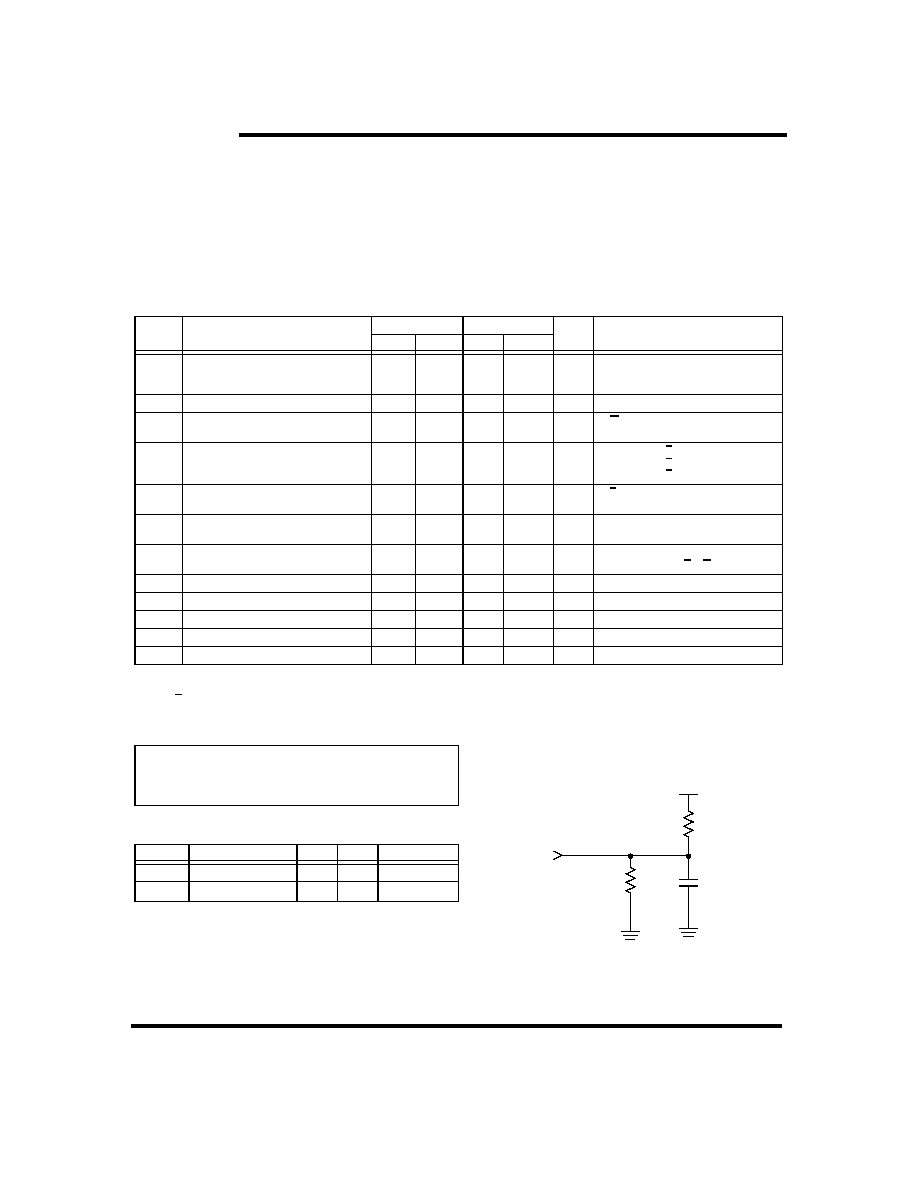
Output Load . . . . . . . . . . . . . . . . . . . . . . . . . . . . . . . . . See Figure 1
SYMBOL
PARAMETER
MAX
UNITS
CONDITIONS
C
IN
Input Capacitance
8
pF
V = 0 to 3V
C
OUT
Output Capacitance
7
pF
V = 0 to 3V
Figure 1: AC Output Loading
480 Ohms
30 pF
255 Ohms
5.0V
INCLUDING
OUTPUT
SCOPE AND
FIXTURE
Note a: Stresses greater than those listed under "Absolute Maximum
Ratings" may cause permanent damage to the device. This is a
stress rating only, and functional operation of the device at condi-
tions above those indicated in the operational sections of this
specification is not implied. Exposure to absolute maximum rat-
ing conditions for extended periods may affect reliability.

STK10C48
September 2003
3
Document Control # ML0002 rev 0.1
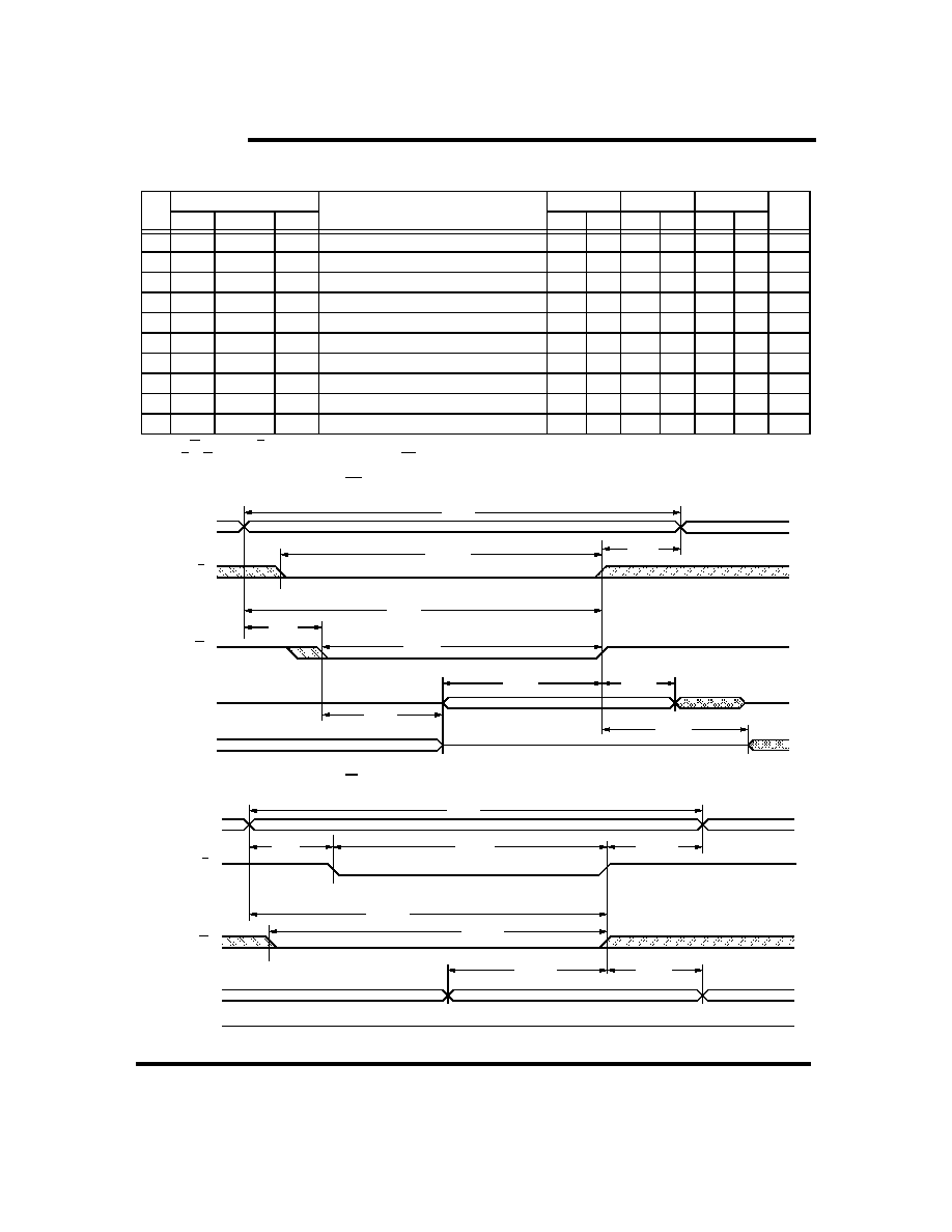
SRAM READ CYCLES #1 & #2
(V
CC
= 5.0V
±
10%)
Note f:
W must be high during SRAM READ cycles and low during SRAM WRITE cycles. NE must be high during entire cycle.
Note g: I/O state assumes E, G < V
IL
, W > V
IH
, and NE
V
IH
; device is continuously selected.
Note h: Measured + 200mV from steady state output voltage.
SRAM READ CYCLE #1: Address Controlled
f, g
SRAM READ CYCLE #2: E Controlled
f
NO.
SYMBOLS
PARAMETER
STK10C48-25
STK10C48-35
STK10C48-45
UNITS
#1, #2
Alt.
MIN
MAX
MIN
MAX
MIN
MAX
1
t
ELQV
t
ACS
Chip Enable Access Time
25
35
45
ns
2
t
AVAV
f
t
RC
Read Cycle Time
25
35
45
ns
3
t
AVQV
g
t
AA
Address Access Time
25
35
45
ns
4
t
GLQV
t
OE
Output Enable to Data Valid
10
15
20
ns
5
t
AXQX
g
t
OH
Output Hold after Address Change
5
5
5
ns
6
t
ELQX
t
LZ
Chip Enable to Output Active
5
5
5
ns
7
t
EHQZ
h
t
HZ
Chip Disable to Output Inactive
10
13
15
ns
8
t
GLQX
t
OLZ
Output Enable to Output Active
0
0
0
ns
9
t
GHQZ
h
t
OHZ
Output Disable to Output Inactive
10
13
15
ns
10
t
ELICCH
e
t
PA
Chip Enable to Power Active
0
0
0
ns
11
t
EHICCL
d, e
t
PS
Chip Disable to Power Standby
25
35
45
ns
DATA VALID
5
t
AXQX
3
t
AVQV
DQ (DATA OUT)
ADDRESS
2
t
AVAV
6
t
ELQX
STANDBY
DATA VALID
8
t
GLQX
4
t
GLQV
DQ (DATA OUT)
E
ADDRESS
2
t
AVAV
G
I
CC
ACTIVE
1
t
ELQV
10
t
ELICCH
11
t
EHICCL
7
t
EHQZ
9
t
GHQZ
STK10C48
September 2003
4
Document Control # ML0002 rev 0.1
SRAM WRITE CYCLES #1 & #2
(V
CC
= 5.0V
±
10%)
Note i:
If W is low when E goes low, the outputs remain in the high-impedance state.
Note j:
E or W must be
V
IH
during address transitions. NE
V
IH
.
SRAM WRITE CYCLE #1: W Controlled
j
SRAM WRITE CYCLE #2: E Controlled
j
NO.
SYMBOLS
PARAMETER
STK10C48-25
STK10C48-35
STK10C48-45
UNITS
#1
#2
Alt.
MIN
MAX
MIN
MAX
MIN
MAX
12
t
AVAV
t
AVAV
t
WC
Write Cycle Time
25
35
45
ns
13
t
WLWH
t
WLEH
t
WP
Write Pulse Width
20
25
30
ns
14
t
ELWH
t
ELEH
t
CW
Chip Enable to End of Write
20
25
30
ns
15
t
DVWH
t
DVEH
t
DW
Data Set-up to End of Write
10
12
15
ns
16
t
WHDX
t
EHDX
t
DH
Data Hold after End of Write
0
0
0
ns
17
t
AVWH
t
AVEH
t
AW
Address Set-up to End of Write
20
25
30
ns
18
t
AVWL
t
AVEL
t
AS
Address Set-up to Start of Write
0
0
0
ns
19
t
WHAX
t
EHAX
t
WR
Address Hold after End of Write
0
0
0
ns
20
t
WLQZ
h, i
t
WZ
Write Enable to Output Disable
10
13
15
ns
21
t
WHQX
t
OW
Output Active after End of Write
5
5
5
ns
PREVIOUS DATA
DATA OUT
E
ADDRESS
12
t
AVAV
W
16
t
WHDX
DATA IN
19
t
WHAX
13
t
WLWH
18
t
AVWL
17
t
AVWH
DATA VALID
20
t
WLQZ
15
t
DVWH
HIGH IMPEDANCE
21
t
WHQX
14
t
ELWH
DATA OUT
E
ADDRESS
12
t
AVAV
W
DATA IN
13
t
WLEH
17
t
AVEH
DATA VALID
HIGH IMPEDANCE
14
t
ELEH
18
t
AVEL
19
t
EHAX
15
t
DVEH
16
t
EHDX
STK10C48
September 2003
5
Document Control # ML0002 rev 0.1
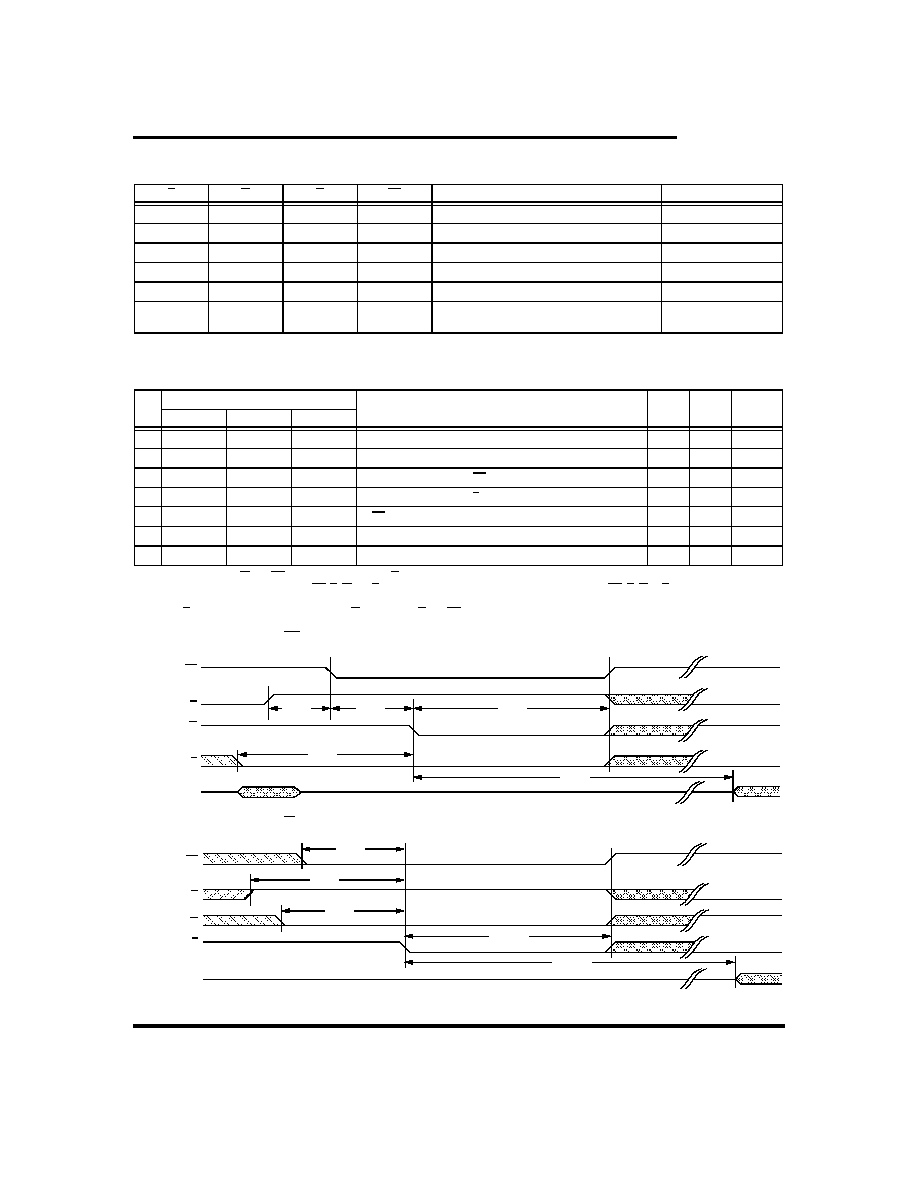
MODE SELECTION
Note k: An automatic RECALL takes place at power up, starting when V
CC
exceeds 4.25V and taking t
RESTORE
.
STORE CYCLES #1 & #2
(V
CC
= 5.0V
±
10%)
Note l:
Measured with W and NE both returned high, and G returned low. STORE cycles are inhibited below 4.0V.
Note m: Once t
WC
has been satisfied by NE, G, W and E, the STORE cycle is completed automatically. Any of NE, G, W or E may be used to terminate
the STORE initiation cycle.
Note n: If E is low for any period of time in which W is high while G and NE are low, then a RECALL cycle may be initiated.
STORE CYCLE #1: W Controlled
n
STORE CYCLE #2: E Controlled
n
E
W
G
NE
MODE
POWER
H
X
X
X
Not Selected
Standby
L
H
L
H
Read SRAM
Active
L
L
X
H
Write SRAM
Active
L
H
L
L
Nonvolatile RECALL
k
Active
L
L
H
L
Nonvolatile STORE
I
CC2
L
L
L
H
L
H
L
X
No Operation
Active
NO.
SYMBOLS
PARAMETER
MIN
MAX
UNITS
#1
#2
Alt.
22
t
WLQX
l
t
ELQX
t
STORE
STORE Cycle Time
10
ms
23
t
WLNH
m
t
ELNH
t
WC
STORE Initiation Cycle Time
20
ns
24
t
GHNL
Output Disable Set-up to NE Fall
0
ns
25
t
GHEL
Output Disable Set-up to E Fall
0
ns
26
t
NLWL
t
NLEL
NE Set-up
0
ns
27
t
ELWL
Chip Enable Set-up
0
ns
28
t
WLEL
Write Enable Set-up
0
ns
HIGH IMPEDANCE
NE
G
W
E
DQ (DATA OUT)
24
t
GHNL
26
t
NLWL
23
t
WLNH
27
t
ELWL
22
t
WLQX
NE
G
W
E
DQ (DATA OUT)
HIGH IMPEDANCE
26
t
NLEL
25
t
GHEL
28
t
WLEL
23
t
ELNH
22
t
ELQX