September 2003
1
Document Control # ML0014 rev 0.1
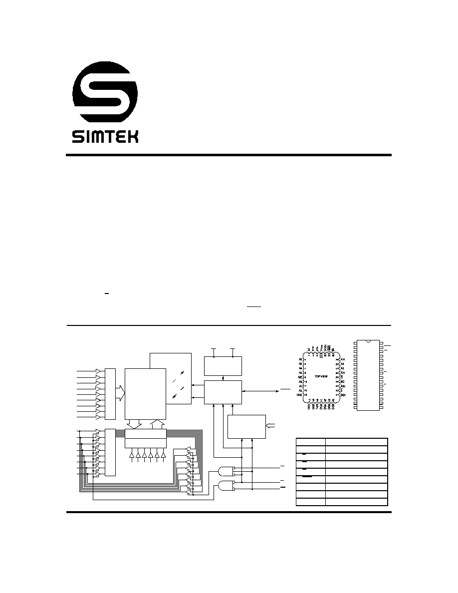
PIN CONFIGURATIONS
V
CAP
A
14
A
12
A
7
A
6
A
5
A
4
A
3
NC
A
2
A
1
A
0
DQ
0
DQ
1
DQ
2
V
SS
V
CCX
HSB
A
13
A
8
A
9
A
11
G
NC
A
10
E
DQ
7
DQ
6
DQ
5
DQ
4
DQ
3
W
1
2
3
4
5
6
7
8
9
10
11
12
13
14
15
16
32
31
30
29
28
27
26
25
24
23
22
21
20
19
18
17
32 - LCC
32 - DIP
32 - SOIC
PIN NAMES
A
0
- A
14
Address Inputs
DQ
0
-DQ
7
Data In/Out
E
Chip Enable
W
Write Enable
G
Output Enable
HSB
Hardware Store Busy (I/O)
V
CCX
Power (+ 5V)
V
CAP
Capacitor
V
SS
Ground
STK14C88
32K x 8 AutoStoreTM nvSRAM
QuantumTrapTM CMOS
Nonvolatile Static RAM
FEATURES
∑ 25ns, 35ns and 45ns Access Times
∑ "Hands-off" Automatic STORE with External
68
µ
F Capacitor on Power Down
∑ STORE to nonvolatile elements Initiated by
Hardware, Software or AutoStoreTM
∑ RECALL to SRAM Initiated by Software or
Power Restore
∑ 10mA Typical I
CC
at 200ns Cycle Time
∑ Unlimited READ, WRITE and RECALL Cycles
∑ 1,000,000 STORE Cycles to nonvolatile ele-
ments (Commercial/Industrial)
∑ 100-Year Data Retention in nonvolatile ele-
ments (Commercial/Industrial)
∑ Single 5V + 10% Operation
∑ Commercial, Industrial and Military Tempera-
tures
∑ 32-Pin SOIC, DIP and LCC Packages
DESCRIPTION
The Simtek STK14C88 is a fast static
RAM
with a
nonvolatile element incorporated in each static
memory cell. The
SRAM
can be read and written an
unlimited number of times, while independent, non-
volatile data resides in the nonvolatile elements.
Data transfers from the
SRAM
to the nonvolatile ele-
ments (the
STORE
operation) can take place auto-
matically on power down. A 68
µ
F or larger capacitor
tied from V
CAP
to ground guarantees the
STORE
operation, regardless of power-down slew rate or
loss of power from "hot swapping". Transfers from
the nonvolatile elements to the
SRAM
(the
RECALL
operation) take place automatically on restoration of
power. Initiation of
STORE
and
RECALL
cycles can
also be software controlled by entering specific read
sequences. A hardware
STORE
may be initiated with
the HSB pin.
BLOCK DIAGRAM
A
0
A
1
A
2
A
3
A
4
A
10
COLUMN I/O
COLUMN DEC
STATIC RAM
ARRAY
512 x 512
ROW DE
CODE
R
INPU
T B
U
FFERS
Quantum Trap
512 x 512
STORE/
RECALL
CONTROL
STORE
RECALL
POWER
CONTROL
A
5
A
6
A
7
A
8
A
9
A
11
A
12
A
13
A
14
DQ
0
DQ
1
DQ
2
DQ
3
DQ
4
DQ
5
DQ
6
DQ
7
SOFTWARE
DETECT
G
E
W
HSB
V
CCX
V
CAP
A
0
- A
13
STK14C88
September 2003
2
Document Control # ML0014 rev 0.1
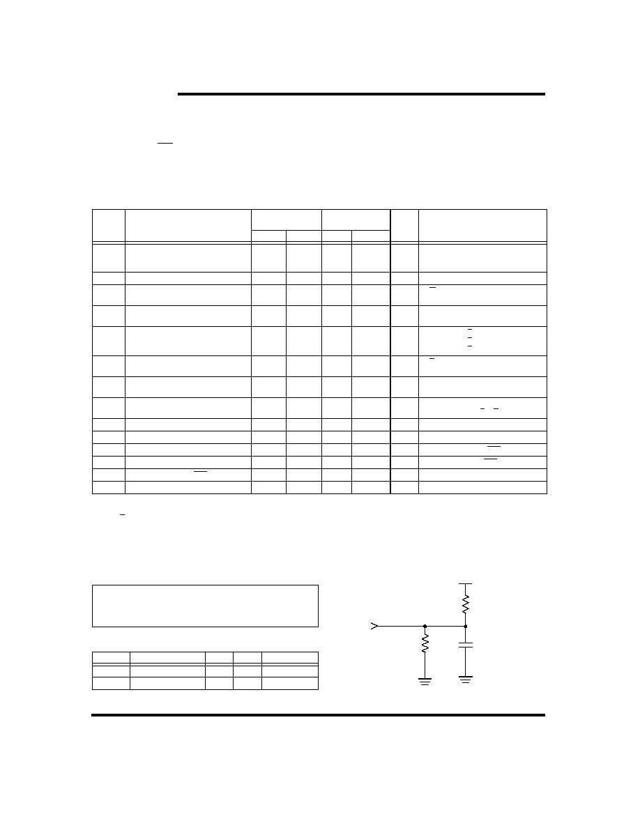
ABSOLUTE MAXIMUM RATINGS
a
Voltage on Input Relative to Ground . . . . . . . . . . . . . ≠0.5V to 7.0V
Voltage on Input Relative to V
SS
. . . . . . . . . .≠0.6V to (V
CC
+ 0.5V)
Voltage on DQ
0-7
or HSB . . . . . . . . . . . . . . . .≠0.5V to (V
CC
+ 0.5V)
Temperature under Bias. . . . . . . . . . . . . . . . . . . . . .≠55
∞
C to 125
∞
C
Storage Temperature . . . . . . . . . . . . . . . . . . . . . . . .≠65
∞
C to 150
∞
C
Power Dissipation . . . . . . . . . . . . . . . . . . . . . . . . . . . . . . . . . . . 1W
DC Output Current (1 output at a time, 1s duration) . . . . . . . 15mA
Note a: Stresses greater than those listed under "Absolute Maximum
Ratings" may cause permanent damage to the device. This is a
stress rating only, and functional operation of the device at con-
ditions above those indicated in the operational sections of this
specification is not implied. Exposure to absolute maximum rat-
ing conditions for extended periods may affect reliability.
DC CHARACTERISTICS
(V
CC
= 5.0V
±
10%)
e
Note b: I
CC1
and I
CC3
are dependent on output loading and cycle rate. The specified values are obtained with outputs unloaded.
Note c: I
CC2
and I
CC4
are the average currents required for the duration of the respective
STORE
cycles (t
STORE
) .
Note d: E
V
IH
will not produce standby current levels until any nonvolatile cycle in progress has timed out.
Note e: V
CC
reference levels throughout this datasheet refer to V
CCX
if that is where the power supply connection is made, or V
CAP
if V
CCX
is con-
nected to ground.
SYMBOL
PARAMETER
COMMERCIAL
INDUSTRIAL/
Military
UNITS
NOTES
MIN
MAX
MIN
MAX
I
CC1
b
Average V
CC
Current
97
80
70
100
85
70
mA
mA
mA
t
AVAV
= 25ns
t
AVAV
= 35ns
t
AVAV
= 45ns
I
CC2
c
Average V
CC
Current during STORE
3
3
mA
All Inputs Don't Care, V
CC
= max
I
CC3
b
Average V
CC
Current at t
AVAV
= 200ns
5V, 25∞C, Typical
10
10
mA
W
(V
CC
≠ 0.2V)
All Others Cycling, CMOS Levels
I
CC4
c
Average V
CAP
Current during
AutoStoreTM Cycle
2
2
mA
All Inputs Don't Care
I
SB1
d
Average V
CC
Current
(Standby, Cycling TTL Input Levels)
30
25
22
31
26
23
mA
mA
mA
t
AVAV
= 25ns, E
V
IH
t
AVAV
= 35ns, E
V
IH
t
AVAV
= 45ns, E
V
IH
I
SB2
d
V
CC
Standby Current
(Standby, Stable CMOS Input Levels)
1.5
1.5
mA
E
(V
CC
≠ 0.2V)
All Others V
IN
0.2V or
(V
CC
≠ 0.2V)
I
ILK
Input Leakage Current
±
1
±
1
µ
A
V
CC
= max
V
IN
= V
SS
to V
CC
I
OLK
Off-State Output Leakage Current
±
5
±
5
µ
A
V
CC
= max
V
IN
= V
SS
to V
CC
, E or G
V
IH
V
IH
Input Logic "1" Voltage
2.2
V
CC
+ .5
2.2
V
CC
+ .5
V
All Inputs
V
IL
Input Logic "0" Voltage
V
SS
≠ .5
0.8
V
SS
≠ .5
0.8
V
All Inputs
V
OH
Output Logic "1" Voltage
2.4
2.4
V
I
OUT
= ≠ 4mA except HSB
V
OL
Output Logic "0" Voltage
0.4
0.4
V
I
OUT
= 8mA except HSB
V
BL
Logic "0" Voltage on HSB Output
0.4
0.4
V
I
OUT
= 3mA
T
A
Operating Temperature
0
70
≠40/-55
85/125
∞
C
AC TEST CONDITIONS
CAPACITANCE
f
(T
A
= 25
∞
C, f = 1.0MHz)
Note f:
These parameters are guaranteed but not tested.
Input Pulse Levels . . . . . . . . . . . . . . . . . . . . . . . . . . . . . . .0V to 3V
Input Rise and Fall Times
. . . . . . . . . . . . . . . . . . . . . . . . . . . . . . . .
5ns
Input and Output Timing Reference Levels . . . . . . . . . . . . . . . 1.5V
Output Load . . . . . . . . . . . . . . . . . . . . . . . . . . . . . . . . See Figure 1
SYMBOL
PARAMETER
MAX
UNITS
CONDITIONS
C
IN
Input Capacitance
5
pF
V = 0 to 3V
C
OUT
Output Capacitance
7
pF
V = 0 to 3V
Figure 1
:
AC Output Loading
480 Ohms
30 pF
255 Ohms
5.0V
INCLUDING
SCOPE AND
OUTPUT
FIXTURE
STK14C88
September 2003
3
Document Control # ML0014 rev 0.1
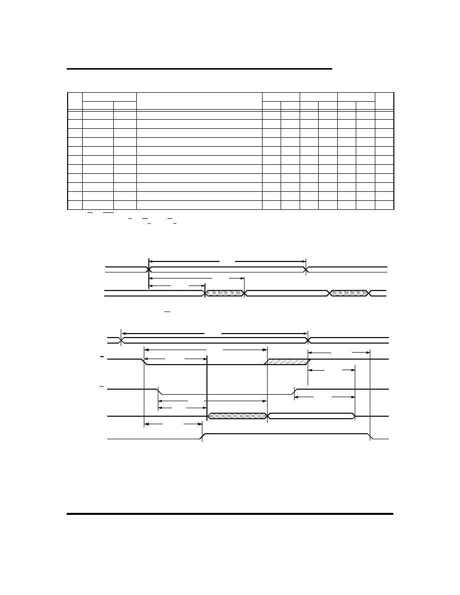
SRAM READ CYCLES #1 & #2
(V
CC
= 5.0V
±
10%)
e
Note g: W and HSB must be high during SRAM READ cycles and low during SRAM WRITE cycles.
Note h: I/O state assumes E and G <
V
IL
and
W >
V
IH
; device is continuously selected.
Note i:
Measured
±
200mV from steady state output voltage.
SRAM READ CYCLE #1: Address Controlled
g,
h
SRAM READ CYCLE #2: E Controlled
g
NO.
SYMBOLS
PARAMETER
STK14C88-25
STK14C88-35
STK14C88-45
UNITS
#1, #2
Alt.
MIN
MAX
MIN
MAX
MIN
MAX
1
t
ELQV
t
ACS
Chip Enable Access Time
25
35
45
ns
2
t
AVAV
g
t
RC
Read Cycle Time
25
35
45
ns
3
t
AVQV
h
t
AA
Address Access Time
25
35
45
ns
4
t
GLQV
t
OE
Output Enable to Data Valid
10
15
20
ns
5
t
AXQX
h
t
OH
Output Hold after Address Change
5
5
5
ns
6
t
ELQX
t
LZ
Chip Enable to Output Active
5
5
5
ns
7
t
EHQZ
i
t
HZ
Chip Disable to Output Inactive
10
13
15
ns
8
t
GLQX
t
OLZ
Output Enable to Output Active
0
0
0
ns
9
t
GHQZ
i
t
OHZ
Output Disable to Output Inactive
10
13
15
ns
10
t
ELICCH
f
t
PA
Chip Enable to Power Active
0
0
0
ns
11
t
EHICCL
f
t
PS
Chip Disable to Power Standby
25
35
45
ns
DATA VALID
5
t
AXQX
3
t
AVQV
DQ (DATA OUT)
ADDRESS
2
t
AVAV
6
t
ELQX
STANDBY
DATA VALID
4
t
GLQV
DQ (DATA OUT)
E
ADDRESS
2
t
AVAV
G
I
CC
ACTIVE
10
t
ELICCH
11
t
EHICCL
7
t
EHQZ
8
t
GLQX
1
t
ELQV
9
t
GHQZ
STK14C88
September 2003
4
Document Control # ML0014 rev 0.1
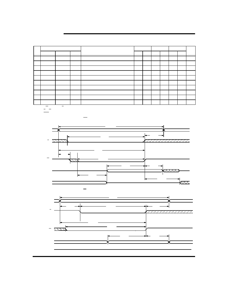
SRAM WRITE CYCLES #1 & #2
(V
CC
= 5.0V
±
10%)
e
Note j:
If W is low when E goes low, the outputs remain in the high-impedance state.
Note k: E or W must be
V
IH
during address transitions.
Note l:
HSB must be high during SRAM WRITE cycles.
SRAM WRITE CYCLE #1: W Controlled
k, l
SRAM WRITE CYCLE #2: E Controlled
k, l
NO.
SYMBOLS
PARAMETER
STK14C88-25
STK14C88-35
STK14C88-45
UNITS
#1
#2
Alt.
MIN
MAX
MIN
MAX
MIN
MAX
12
t
AVAV
t
AVAV
t
WC
Write Cycle Time
25
35
45
ns
13
t
WLWH
t
WLEH
t
WP
Write Pulse Width
20
25
30
ns
14
t
ELWH
t
ELEH
t
CW
Chip Enable to End of Write
20
25
30
ns
15
t
DVWH
t
DVEH
t
DW
Data Set-up to End of Write
10
12
15
ns
16
t
WHDX
t
EHDX
t
DH
Data Hold after End of Write
0
0
0
ns
17
t
AVWH
t
AVEH
t
AW
Address Set-up to End of Write
20
25
30
ns
18
t
AVWL
t
AVEL
t
AS
Address Set-up to Start of Write
0
0
0
ns
19
t
WHAX
t
EHAX
t
WR
Address Hold after End of Write
0
0
0
ns
20
t
WLQZ
i, j
t
WZ
Write Enable to Output Disable
10
13
15
ns
21
t
WHQX
t
OW
Output Active after End of Write
5
5
5
ns
PREVIOUS DATA
DATA OUT
E
ADDRESS
12
t
AVAV
W
16
t
WHDX
DATA IN
19
t
WHAX
13
t
WLWH
18
t
AVWL
17
t
AVWH
DATA VALID
20
t
WLQZ
15
t
DVWH
HIGH IMPEDANCE
21
t
WHQX
14
t
ELWH
DATA IN
12
t
AVAV
16
t
EHDX
13
t
WLEH
19
t
EHAX
18
t
AVEL
17
t
AVEH
DATA VALID
15
t
DVEH
HIGH IMPEDANCE
14
t
ELEH
DATA OUT
E
ADDRESS
W
DATA IN

STK14C88
September 2003
5
Document Control # ML0014 rev 0.1
HARDWARE MODE SELECTION
Note m: HSB STORE operation occurs only if an SRAM WRITE has been done since the last nonvolatile cycle. After the STORE (if any) completes,
the part will go into standby mode, inhibiting all operations until HSB rises.
HARDWARE STORE CYCLE
(V
CC
= 5.0V
±
10%)
e
Note n: E and G low and W high for output behavior.
Note o: t
RECOVER
is only applicable after t
STORE
is complete.
HARDWARE STORE CYCLE
E
W
HSB
A
13
- A
0
(hex)
MODE
I/O
POWER
NOTES
H
X
H
X
Not Selected
Output High Z
Standby
L
H
H
X
Read SRAM
Output Data
Active
t
L
L
H
X
Write SRAM
Input Data
Active
X
X
L
X
Nonvolatile
STORE
Output High Z
l
CC2
m
NO.
SYMBOLS
PARAMETER
STK14C88
UNITS NOTES
Standard
Alternate
MIN
MAX
22
t
STORE
t
HLHZ
STORE Cycle Duration
10
ms
i, n
23
t
DELAY
t
HLQZ
Time Allowed to Complete SRAM Cycle
1
µ
s
i, n
24
t
RECOVER
t
HHQX
Hardware STORE High to Inhibit Off
700
ns
n, o
25
t
HLHX
Hardware STORE Pulse Width
15
ns
26
t
HLBL
Hardware STORE Low to STORE Busy
300
ns
DATA VALID
HSB (IN)
DATA VALID
25
t
HLHX
23
t
DELAY
22
t
STORE
24
t
RECOVER
HIGH IMPEDANCE
26
t
HLBL
HIGH IMPEDANCE
DQ (DATA OUT)
HSB (OUT)