 | –≠–ª–µ–∫—Ç—Ä–æ–Ω–Ω—ã–π –∫–æ–º–ø–æ–Ω–µ–Ω—Ç: HS7541AA | –°–∫–∞—á–∞—Ç—å:  PDF PDF  ZIP ZIP |

HS7541A
12-Bit CMOS Multiplying DAC
© Copyright 2000 Sipex Corporation
1
DESCRIPTION...
The HS7541A is a low≠cost, high stability monolithic 12≠bit CMOS 4≠quadrant multiplying DAC.
It is constructed using a proprietary low≠TCR thin≠film process that requires no laser≠trimming
to achieve 12≠bit performance. The HS7541A is a superior pin≠compatible replacement for the
industry standard 7541 and AD7541A. It is available in both commercial and industrial
temperature ranges. It operates with +5V to +15V power supply voltages. It is available in 18≠
pin plastic DIP and SOIC, and 20≠pin PLCC packages.
s
±
0.5 LSB DNL and INL
s
High Stability, Segmented Architecture
(3 MSB's)
s
Proprietary, Low TCR Thin≠Film
Resistor Technology
s
Low Sensitivity to Output Amplifier
Offset
s
2KV ESD Protection on All Digital
Inputs
s
Operates With +5V to +15V Power
Supplies
s
AD7541/7541A Replacement
s
Low Cost
D
11
(MSB) [4]
D
10
[5]
D
9
[6]
D
8
[7]
D
7
[8]
D
6
[9]
D
5
[10]
D
4
[11]
D
3
[12]
D
2
[13]
D
1
[14]
D
0
(LSB) [15]
R
FB
[18]
V
DD
[16] GND [3]
V
REF
[17]
20K
10K
20K
10K
20K
10K
20K
10K
20K
10K
20K
10K
20K
10K
20K
10K
20K
10K
20K
10K
20K
10K
20K
20K
I
O2
[2]
I
O1
[1]
10K
Æ
HS7541A
12≠Bit CMOS Multiplying DAC
HS7541A
12-Bit CMOS Multiplying DAC
© Copyright 2000 Sipex Corporation
2
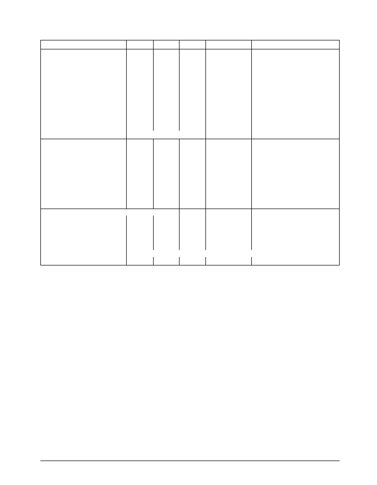
SPECIFICATIONS
(T
A
=25
∞
C; V
DD
=+15V, V
REF
= +10V; I
O1
= I
O2
= GND = 0V; unipolar unless otherwise noted.)
PARAMETER
MIN.
TYP.
MAX.
UNIT
CONDITIONS
STATIC PERFORMANCE
Resolution
12
Bits
Integral Non-Linearity
Note 6
-AJ, -AA
±
1.0
LSB
Note 5; 11-bit relative accuracy
-AK, -AB
±
0.5
LSB
Note 5; 12-bit relative accuracy
Differential Non-Linearity
Note 7
-AJ, -AA
±
1.0
LSB
Note 5; Monotonic to 12-bits
-AK, -AB
±
0.5
LSB
Note 5; Monotonic to 12-bits
Gain Error
Note 17
-AJ, -AA
±
6
LSB
±
8
LSB
Note 5
-AK, -AB
±
3
LSB
±
5
LSB
Note 5
Output Leakage Current
±
5
nA
At I
O1
(Pin 1); Note 18
±
10
nA
Note 5
AC PERFORMANCE CHARACTERISTICS
Output Amplifier HOS-050;
Note 8
Propagation Delay
100
ns
Note 9
Current Settling Time
0.6
µ
s
Full scale transition; Note 10
Output Capacitance
CI
O1
(Pin 16)
200
pF
Note 5; data inputs V
IH
CI
O2
(Pin 15)
70
pF
Note 5; data inputs V
IH
CI
O1
(Pin 16)
70
pF
Note 5; data inputs V
IL
CI
O2
(Pin 15)
200
pF
Note 5; data inputs V
IL
Glitch Energy
1,000
nVs
Note 11
Multiplying Feedthrough Error
1.0
mV
P-P
Measured at output I
O1
;
Note 12
0.1
mV
P-P
Measured at output I
O1
;
Note 13
STABILITY
Gain Error TC
±
1.0
ppm/
∞
C
INL TC
±
0.1
ppm/
∞
C
DNL TC
±
0.1
ppm/
∞
C
Power Supply Rejection Ratio
±
0.02
%/%
V
DD
= 14 to 16V
REFERENCE INPUT
Input Resistance
7
10
15
K
Pin 19 to GND
Input Resistance TC
±
150
ppm/
∞
C
Voltage Range
±
25
Volts
Note 5 and 14
CAUTION:
ESD (ElectroStatic Discharge) sensitive
device. Permanent damage may occur on
unconnected devices subject to high energy
electrostatic fields. Unused devices must be
stored in conductive foam or shunts.
Personnel should be properly grounded prior
to handling this device. The protective foam
should be discharged to the destination
socket before devices are removed.
ABSOLUTE MAXIMUM RATINGS
(T
A
= 25
∞
C unless otherwise noted.)
These are stress ratings only and functional operation of the device
at these or any other above those indicated in the operation
sections of the specifications below is not implied. Exposure to
absolute maximum rating conditions for extended periods of time
may affect reliability.
V
DD
to GND .................................................................. ≠0.3V, +17V
Digital Input Voltage to GND ................................. ≠0.3V, V
DD
+0.3V
V
REF
or V
RFB
to GND ................................................................
±
25V
Output Voltage (Pin 1, Pin 2) ................................ ≠0.3V, V
DD
+0.3V
Power Dissipation (Any Package to +75
∞
C) ........................ 450mW
Derates above 75
∞
C by ...................................................... 6mW/
∞
C
Dice Junction Temperature ................................................. +150
∞
C
Storage Temperature ............................................ ≠65
∞
C to +150
∞
C
Lead Temperature (Soldering, 60 seconds) ........................ +300
∞
C
HS7541A
12-Bit CMOS Multiplying DAC
© Copyright 2000 Sipex Corporation
3
SPECIFICATIONS (continued)
(T
A
=25
∞
C; V
DD
=+15V, V
REF
= +10V; I
O1
= I
O2
= GND = 0V; unipolar unless otherwise noted.)
PARAMETER
MIN.
TYP.
MAX.
UNIT
CONDITIONS
DIGITAL INPUTS
Logic Levels
V
IH
2.4
V
DD
Volts
2.4
Volts
Note 5
V
IL
-0.3
0.8
Volts
0.8
Volts
Note 5
Input Current
±
1.0
µ
A
V
IN
= 0V or V
DD
±
10
µ
A
Note 5 and 15
Input Capacitance
V
IN
= 0; Note 5 and 14
Bits 1--12
8
pF
Note 5
Coding
Unipolar
Binary
Bipolar
Offset Binary
POWER REQUIREMENTS
Voltage Range
+5
+15
Volts
Note 16
+16
Volts
Note 5
Supply Current
2.0
2.5
mA
All digital inputs V
IL
or V
IH
2.5
mA
Note 5; all digital inputs V
IL
or
V
IH
0.2
0.5
mA
All digital inputs 0V or 5V to
V
DD
1.0
mA
Note 5; all digital inputs 0V or
5V to V
DD
ENVIRONMENTAL AND MECHANICAL
Operating Temperature
-AK, -AJ
0
+70
∞
C
-AB, -AA
-40
+85
∞
C
Storage Temperature
-65
+150
∞
C
Package
-AK, -AJ
18-pin plastic DIP, 20-pin PLCC, 18≠pin SOIC
Notes and Cautions:
1.
Do not apply voltages higher than VDD or less than GND potential on any terminal other than V
REF
or V
RFB
.
2.
The digital inputs are diode-clamp protected against ESD damage. However, permanent damage may occur
on unprotected units from high-energy electrostatic fields. Keep units in conductive foam at all times until
ready to use.
3.
Use proper anti-static handling procedures.
4.
Stresses above those listed under "Absolute Maximum Ratings" may cause permanent damage to the
device. This is a stress rating only and functional operation at or above these specifications is not implied.
Exposure to the above maximum rated conditions for extended periods may affect device reliability.
5.
From T
MIN
to T
MAX
.
6.
Integral Non-linearity is measured as the arithmetic mean value of the magnitudes of the greatest positive
deviation and the greatest negative deviation from the theoretical value of any given input combination.
7.
Differential Non-linearity is the deviation of an output step from the theoretical value of 1 LSB for any two
adjacent digital input codes.
8.
AC performance characteristics are included for design guidance only and are subject to sample testing only.
9.
R
L
= 100
, C
EXT
= 13pF; all data inputs 0V to V
DD
or V
DD
to 0V; from 50% digital input change to 90% of final
analog output.
10.
Settling to
±
0.01% FSR (strobed); all data inputs 0V to V
DD
or V
DD
to 0V.
11.
V
REF
= 0V, DAC register alternatively loaded with all 0's and all 1's.
12.
V
REF
= 20V
P-P
; F = 10kHz sinewave.
13.
V
REF
= 20V
P-P
; F = 1kHz sinewave.
14.
Guaranteed by design, but not production tested.
15.
Logic inputs are MOS gates. I
IN
typically is less than 1nA @ 25
∞
C.
16.
Accuracy is guaranteed at V
DD
= +15V only.
17.
Measured using internal feedback resistor with DAC loaded with all 1's.
18.
All digital inputs = 0V.

HS7541A
12-Bit CMOS Multiplying DAC
© Copyright 2000 Sipex Corporation
4
PIN ASSIGNMENTS
18≠Pin Plastic DIP and SOIC
Pin 1 -- I
O1
-- Inverted Current Output.
Pin 2 -- I
O2
-- Current Output.
Pin 3 -- GND -- Analog Ground.
Pin 4 -- D
11
(MSB) -- Data Bit 11 (Most Significant
Bit).
Pin 5 -- D
10
-- Data Bit 10.
Pin 6 -- D
9
-- Data Bit 9.
Pin 7 -- D
8
-- Data Bit 8.
Pin 8 -- D
7
-- Data Bit 7.
Pin 9 -- D
6
-- Data Bit 6.
Pin 10 -- D
5
-- Data Bit 5.
Pin 11 -- D
4
-- Data Bit 4.
Pin 12 -- D
3
-- Data Bit 3.
Pin 13 -- D
2
-- Data Bit 2.
Pin 14 -- D
1
-- Data Bit 1.
Pin 15 -- D
0
(LSB) -- Data Bit 0 (Least Significant
Bit).
Pin 16 -- V
DD
-- +5V to +15V Power Supply.
Pin 17 -- V
REF
-- Voltage Reference Input.
Pin 18 -- R
FB
-- Feedback Resistor.
20≠Pin Plastic LCC
Pin 1 -- I
O1
-- Inverted Current Output.
Pin 2 -- I
O2
-- Current Output.
Pin 3 -- GND -- Analog Ground.
Pin 4 -- N.C. -- No Connection.
Pin 5 -- D
11
(MSB) -- Data Bit 11 (Most
Significant Bit).
Pin 6 -- D
10
-- Data Bit 10.
Pin 7 -- D
9
-- Data Bit 9.
Pin 8 -- D
8
-- Data Bit 8.
Pin 9 -- D
7
-- Data Bit 7.
Pin 10 -- D
6
-- Data Bit 6.
Pin 11 -- D
5
-- Data Bit 5.
Pin 12 -- D
4
-- Data Bit 4.
Pin 13 -- D
3
-- Data Bit 3.
Pin 14 -- D
2
-- Data Bit 2.
Pin 15 -- D
1
-- Data Bit 1.
Pin 16 -- D
0
(LSB) -- Data Bit 0 (Least Signifi-
cant Bit).
Pin 17 -- N.C. -- No Connection.
Pin 18 -- V
DD
-- +5V to +15V Power Supply.
Pin 19 -- V
REF
-- Voltage Reference Input.
Pin 20 -- R
FB
-- Feedback Resistor.
FEATURES...
The HS7541A is a low≠cost, high stability mono-
lithic 12≠bit CMOS 4≠quadrant multiplying
DAC. It is constructed using a proprietary low≠
TCR thin≠film process that requires no laser≠
trimming to achieve 12≠bit performance. With
its inherent high stability and a segmented (de-
coded) DAC architecture, the HS7541A retains
its performance over time and temperature. To
further improve reliability, all digital inputs are
protected against 2KV ESD. Each DAC is fully
characterized by all≠codes testing to eliminate
any hidden errors.
The HS7541A consists of a highly stable thin≠
film R≠2R ladder network and twelve NMOS
current switches (please refer to the Block Dia-
gram on the first page of this data sheet). The
switches are temperature compensated, and their
"on" resistances are binarily scaled so that the
voltage drop across each switch is identical,
which contributes to the stability of the DAC.
The internal feedback resistor used in the output
current≠to≠voltage conversion by an external
op amp is matched to the R≠2R ladder.
CIRCUIT DESCRIPTION
General
The HS7541A is a 12-bit multiplying D/A con-
verter consisting of a highly stable, SiChrome
thin-film R-2R resistor ladder network, and
twelve pairs of NMOS current-steering switches
on a monolithic chip.
A simplified circuit of the HS7541A is shown in
Figure 1. The R-2R inverted ladder binarily
divides the input currents that are switched
between the I
OUT1
and I
OUT2
bus lines. This switch-
ing allows a constant current to be maintained in
each ladder leg independent of the input code.

HS7541A
12-Bit CMOS Multiplying DAC
© Copyright 2000 Sipex Corporation
5
V
REF
10K
20K
D
11
(MSB)
D
1
D
2
D
0
(LSB)
I
OUT2
I
OUT1
R
FB
10K
10K
20K
20K
20K
20K
S
1
S
2
S
11
S
0
Switches shown for digital inputs "high"
R = 10K
I
LEAKAGE
30pF
R
FEEDBACK
I
OUT1
I
LEAKAGE
85pF
I
OUT2
1/4096
I
REF
V
REF
R = 10K
The twelve output current-steering switches are
in series with the R-2R ladder, and therefore,
can introduce bit errors. It is essential then, that
the switch "on" resistance be binarily scaled so
that the voltage drop across each switch remains
constant. If, for example, switch S
0
of Figure 1
was designed with an "on" resistance of 10
ohms, switch S
1
for 20 ohms, etc., then with a
10V reference input, the current through S
0
is
0.5mA, S
1
is 0.25mA, etc.; a constant 5mV drop
will then be maintained across each switch.
To further insure accuracy across the full tem-
perature range, permanently "on" MOS switches
are included in series with the feedback resistor
and the R-2R ladder's terminating resistor. These
series switches are equivalently scaled to two
times switch S
11
(MSB) and to switch S
0
(LSB)
respectively to maintain constant relative volt-
age drops with varying temperature. During any
testing of the resistor ladder or R
FB
(such as
incoming inspection), V
DD
must be present to
turn "on" these series switches.
Figure 3. Equivalent Circuit ≠ All Inputs High
Figure 1. Simplified DAC Circuit
2001V ESD Protection
In the design of the HS7541A's data inputs,
2001V ESD resistance has been incorporated
through careful layout and the inclusion of input
protection circuitry.
Equivalent Circuit Analysis
Figures 2 and 3 show the equivalent circuits for all
digital inputs LOW and HIGH respectively. The
reference current is switched to I
OUT2
when all inputs
are LOW, and to I
OUT1
when all inputs are HIGH.
The I
LEAKAGE
current source is the combination of
surface and junction leakages to the substrate; the
1/4096 current source represents the constant 1-bit
current drain through the ladder terminating resis-
tor. The output capacitance is dependent upon the
digital input code, and therefore varies between the
low and high values.
Output Impedance
The output resistance, as in the case of the output
capacitance, varies with the digital input code.
The resistance, looking back into the I
OUT1
ter-
R = 10K
I
LEAKAGE
30pF
R
FEEDBACK
I
OUT1
I
LEAKAGE
85pF
I
OUT2
1/4096
I
REF
V
REF
R = 10K
Figure 2. Equivalent Circuit ≠ All Inputs Low
V
REF
(≠10V)
D
11
(MSB)
D
0
(LSB)
INPUT
DATA
2K
GAIN TRIM
1K
GAIN TRIM
15pF
+15V
≠15V
V
OUT
≠
+
R
FB
I
O1
I
O2
GND
V
REF
V
DD
+15V
4
15
3
2
1
18
16
17
HS7541A
Figure 4. Unipolar Operation