
1
Date: 5/11/05
SP1490E/1491E Full Duplex RS-485 Transceivers
© Copyright 2004 Sipex Corporation
SP1490E/SP1491E
Full Duplex RS-485 Transceivers
+5V Only
Low Power BiCMOS
Driver/Receiver Enable (SP1491E)
RS-485 and RS-422 Drivers/Receivers
Pin Compatible with SN75179
(SP1490E)
Pin Compatible with SN75180
(SP1491E)
Improved ESD Specifications
±15kV Human Body Model
±15kV IEC1000-4-2 Air Discharge
±8kV IEC1000-4-2 Contact Discharge
SP1490E
SP1491E
Æ
1
2
3
4
5
6
7
8
VCC
SP1490E
8 Pin - nSOIC
DI
Y
RO
B
A
Z
GND
DESCRIPTION
FEATURES
APPLICATIONS
Industial Networks Telecom
Motor Control
The SP1490E is a low power differential line driver/receiver meeting RS-485 and RS-422
standards up to 20Mbps. The SP1491E is identical to the SP1490E with the addition of driver
and receiver tri-state enable lines. Both products feature ±200mV receiver input sensitivity,
over wide common mode range. The SP1490E is available in 8-pin plastic DIP and 8-pin
NSOIC packages for operation over the commercial and industrial temperature ranges. The
SP1491E is available in 14-pin DIP and 14-pin NSOIC packages for operation over the
commercial and industrial temperature ranges.
BLOCK DIAGRAM
HVAC/ Building Control
1
2
3
4
5
6
7
8
R
D
Vcc
GND
RO
DI
A
B
Z
Y
6
1
2
3
4
5
7
8
Vcc
GND
RO
DI
A
B
Z
Y
R
D
9
10
11
12
13
14
NC
REB
DE
GND
NC
NC
2
Date: 5/11/05
SP1490E/1491E Full Duplex RS-485 Transceivers
© Copyright 2004 Sipex Corporation
ABSOLUTE MAXIMUM RATINGS
These are stress ratings only and functional operation of the device at
these ratings or any other above those indicated in the operation sections
of the specifications below is not implied. Exposure to absolute maximum
rating conditions for extended periods of time may affect reliability.
V
CC
...................................................................................................+7V
Input Voltages
Drivers................................................-0.5V to (V
CC
+0.5V)
Receivers..................................................................±14V
Output Voltages
Drivers......................................................................±14V
Receivers...........................................-0.5V to (V
CC
+0.5V)
Storage Temperature....................................................-65∞C to +150∞
Power Dissipation.....................................................................1000mW
T
MIN
to T
MAX
and V
CC
= 5V ± 5% unless otherwise noted.
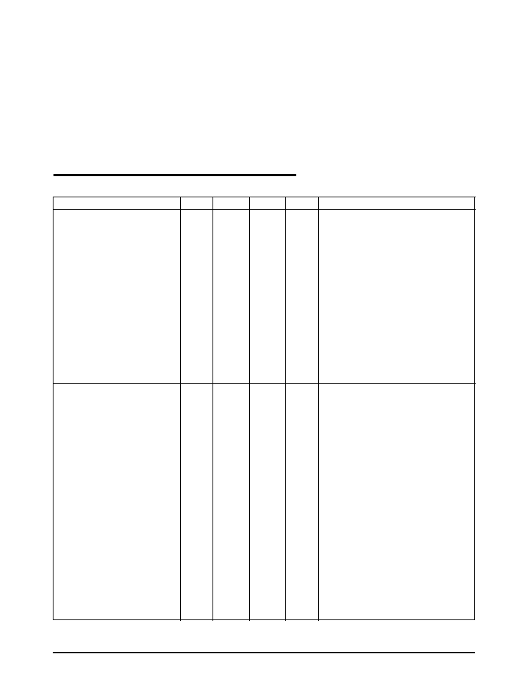
PARAMETERS
MIN.
TYP.
MAX.
UNITS
CONDITIONS
SP1490E/1491E DRIVER
DC Characteristics
Differential Output Voltage
3.5
V
CC
Volts
Unloaded; R = ;
see figure 1
Differential Output Voltage
2
V
CC
Volts
With Load; R = 50; (RS422);
see figure 1
Differential Output Voltage
1.5
V
CC
Volts
With Load; R = 27; (RS485);
see figure 1
Change in Magnitude of Driver
Differential Output Voltage for
Complimentary States
0.2
Volts
R = 27 or R = 50;
see figure 1
Driver Common-Mode
Output Voltage
3
Volts
R = 27 or R = 50;
see figure 1
Input High Voltage
2.0
Volts
Applies to D
Input Low Voltage
0.8
Volts
Applies to D
Input Current
±10
µA
Applies to D
Driver Short-Circuit Current
V
OUT
= HIGH
±250
mA
-7V V
O
+12V
V
OUT
= LOW
±250
mA
-7V V
O
+12V
SP1490E/1491E DRIVER
AC Characteristics
Maximum Data Rate
20
Mbps
Driver Input to Output
30
40
ns
t
R/F
; R
DIFF
= 54, C
L1
= C
L2
= 100pF;
see figures 3 and 6
Driver Input to Output
30
40
ns
t
R/F
; R
DIFF
= 54, C
L1
= C
L2
= 100pF;
see figures 3 and 6
Driver Skew
5
ns
see figures 3 and 6,
t
R/F
= | t
DPLH
- t
DPHL
|
Driver Rise or Fall Time 8
20
ns
From 10% to 90%; R
DIFF
= 54,
SP1491E only
C
L1
= C
L2
= 100pF;
see figures 3 and 6
t
R/F
Driver Enable to Output High
20
70
ns
C
L1
= C
L2
= 100pF;
see figures
4 and 7;
S
2
closed
Driver Enable to Output Low
40
70
ns
C
L1
= C
L2
= 100pF;
see figures
4 and 7;
S
1
closed
Driver Disable Time from Low
40
70
ns
C
L1
= C
L2
= 100pF;
see figures
4 and 7;
S
1
closed
Driver Disable Time from High
40
70
ns
C
L1
= C
L2
= 100pF;
see figures
4 and 7;
S
2
closed
ELECTRICAL CHARACTERISTICS

3
Date: 5/11/05
SP1490E/1491E Full Duplex RS-485 Transceivers
© Copyright 2004 Sipex Corporation
SP1490E/1491E RECEIVER
DC Characteristics
Differential Input Threshold
0.2
+0.2
Volts
-7V V
CM
12V
Input Hysteresis
70
mV
V
CM
= 0V
Output Voltage High
3.5
Volts
I
O
= -4mA, V
ID
= +200mV
Output Voltage Low
0.4
Volts
I
O
= +4mA, V
ID
= -200mV
Input Resistance
12
15
k
-7V V
CM
12V (1 unit load)
Input Current (A, B); V
IN
= 12V
±1.0
mA
V
IN
= 12V
Input Current (A, B); V
IN
= -7V
-0.8
mA
V
IN
= -7V
Short-Circuit Current
85
mA
0V V
O
V
CC
PARAMETERS
MIN.
TYP.
MAX.
UNITS
CONDITIONS
SP1490E/1491E RECEIVER
AC Characteristics
Maximum Data Rate
20
Mbps
Receiver Input to Output
20
45
50
ns
t
PLH
; R
DIFF
= 54,
C
L1
15pF
RO
A
B
A
B
DI
DE
3V
C
L2
R
DIFF
500
C
L
Output
Under
Test
S
1
S
2
V
CC
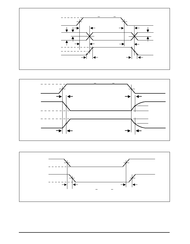
Figure 3. Driver/Receiver Timing Test Circuit
Figure 4. Driver Timing Test Load #2 Circuit
A
B
R
R
V
OD
V
OC
1K
1K
C
RL
Receiver
Output
S
1
S
2
Test Point
V
CC
Figure 1. Driver DC Test Load Circuit
Figure 2. Receiver Timing Test Load Circuit
C
L1
= C
L2
=
100pF;
Figures 3 & 8
Receiver Input to Output
20
45
50
ns
t
PHL
; R
DIFF
= 54,
C
L1
= C
L2
=
100pF;
Figures 3 & 8
Diff. Receiver Skew It
PLH
-t
PHL
I
5
10
ns
R
DIFF
= 54; C
L1
= C
L2
= 100pF;
Receiver Tplh/Tphl
40
70
ns
POWER REQUIREMENTS
Supply Voltage
+4.75
+5.25
Volts
Supply Current
900
µA
ENVIRONMENTAL AND
MECHANICAL
Operating Temperature
Commercial (_C_)
0
+70
∞C
Industrial (_E_)
-40
+85
∞C
Storage Temperature
-65
+150
∞C
Package
Plastic DIP (_S_)
NSOIC (_N)
SPECIFICATIONS (continued)
T
MIN
to T
MAX
and V
CC
= 5V ± 5% unless otherwise noted.
4
Date: 5/11/05
SP1490E/1491E Full Duplex RS-485 Transceivers
© Copyright 2004 Sipex Corporation
Figure 6. Driver Propagation Delays
+3V
0V
DE
5V
V
OL
A, B
0V
1.5V
1.5V
t
ZL
t
ZH
f = 1MHz; t
R
< 10ns; t
F
< 10ns
V
OH
A, B
2.3V
2.3V
t
LZ
t
HZ
0.5V
0.5V
Output normally LOW
Output normally HIGH
Figure 7. Driver Enable and Disable Times SP1491E only
Figure 8. Receiver Propagation Delays
+3V
+3V
0V
0V
DI
DI
B
A
DRIVER
DRIVER
OUTPUT
OUTPUT
V
O
+
DIFFERENTIAL
DIFFERENTIAL
OUTPUT
OUTPUT
V
A
≠ V
B
0V
0V
V
O
≠
1.5V
1.5V
1.5V
t
PLH
PLH
t
R
t
F
f = 1MHz; t
f = 1MHz; t
R
< 10ns; t
< 10ns; t
F
F
< 10ns
< 10ns
V
O
1/2V
1/2V
O
1/2V
1/2V
O
t
PHL
PHL
t
DPLH
DPLH
t
DPHL
DPHL
t
SKEW =
SKEW =
|
t
DPLH -
DPLH -
t
DPHL
DPHL
|
V
OH
V
OL
R
1.5V
1.5V
t
PHL
f = 1MHz; t
R
< 10ns; t
F
< 10ns
OUTPUT
V
0D2
+
V
0D2
≠
A ≠ B
0V
0V
t
PLH
INPUT
t
SKEW =
|
t
PHL -
t
PLH
|
5
Date: 5/11/05
SP1490E/1491E Full Duplex RS-485 Transceivers
© Copyright 2004 Sipex Corporation
The SP1490E and SP1491E are full-duplex dif-
ferential transceivers that meet the requirements
of RS-485 and RS-422. Fabricated with a Sipex
proprietary BiCMOS process, both products
require a fraction of the power of older bipolar
designs.
The RS-485 standard is ideal for multi-drop
applications or for long-distance interfaces.
RS-485 allows up to 32 drivers and 32 receivers
to be connected to a data bus, making it an ideal
choice for multi-drop applications. Since the
cabling can be as long as 4,000 feet, RS-485
transceivers are equipped with a wide (-7V to
+12V) common mode range to accommodate
ground potential differences. Because RS-485
is a differential interface, data is virtually
immune to noise in the transmission line.
Driver...
The drivers for both the SP1490E and SP1491E
have differential outputs. The typical voltage
output swing with no load will be 0 volts to +5
volts. With worst case loading of 54
across the
differential outputs, the driver can maintain
greater than 1.5V voltage levels.
The driver of the SP1491E has a driver enable
control line which is active high. A logic high
on DE (pin 4) of the SP1491E will enable
the differential driver outputs. A logic low
on DE (pin 4) of the SP1491E will tri-state the
driver outputs. The SP1490E does not have a
driver enable.
Receiver...
The receivers for both the SP1490E and
SP1491E have differential inputs with an input
sensitivity as low as
±200mV. Input impedance
of the receivers is typically 15K
(12K mini-
mum). A wide common mode range of -7V to
+12V allows for large ground potential differ-
ences between systems. The receivers for both
the SP1490E and SP1491E are equipped with
the fail-safe feature. Fail-safe guarantees that
the receiver output will be in a high state when
the input is left unconnected and floating.
The receiver of the SP1491E has a receiver
enable control line which is active low. A logic
low on REB (pin 3) of the SP1491E will enable
the differential receiver. A logic high on REB
(pin 3) of the SP1491E will tri-state the re-
ceiver.
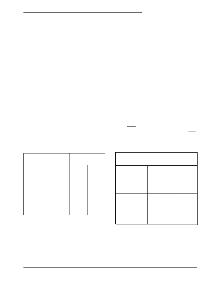
S
T
U
P
N
I
S
T
U
P
T
U
O
E
D
y
l
n
o
E
1
9
4
1
P
S
I
D
Y
Z
1
1
0
1
0
x
1
0
z
0
1
z
INPUTS
OUTPUTS
RE
SP1491E
A-B
R
0
0
0
1
+0.2V
-0.2V
open
x
1
0
1
z
Transmit Function Truth Table
Recieve Function Truth Table
only
DETAILED DESCRIPTION