 | –≠–ª–µ–∫—Ç—Ä–æ–Ω–Ω—ã–π –∫–æ–º–ø–æ–Ω–µ–Ω—Ç: SP1674BJ | –°–∫–∞—á–∞—Ç—å:  PDF PDF  ZIP ZIP |
SP574B/674B/1674B/774B
12≠Bit Sampling A/D Converters
© Copyright 2000 Sipex Corporation
1
s
Complete Monolithic 12≠Bit A/D Converters
with Sample≠Hold, Reference, Clock and Tri≠
state Outputs
s
Full Nyquist Sampling at All Sample Rates
s
Choice of Sampling Rates -- 40kHz, 66kHz,
100kHz or 125kHz
s
Low Power Dissipation -- 110mW
s
12≠Bit Linearity Over Temperature
s
Commercial, Industrial and Military Tempera-
ture Ranges
s
Next≠Generation Replacement for 574A, 674A,
1674A, 774A Devices
1
14
13
12
11
10
9
8
7
6
5
4
3
2
28
15
16
17
18
19
20
21
22
23
24
25
26
27
STS
DB11
DB10
DB9
DB8
DB7
DB6
DB5
DB4
DB3
DB2
DB1
DB0
DGND
VLOGIC 12/8
CS
A0
R/C
CE
VCC
REF
OUT
AGND
REF
IN
VEE
BIP
OFF
10V
IN
20V
IN
NIBBLE A
NIBBLE B
NIBBLE C
THREE≠STATE BUFFERS AND CONTROL
N/C
7.5K
15K
15K
7.5K
7.5K
OFFSET/GAIN
TRIM
12≠BIT
CAPACITANCE
DAC
COMP
REF
CONTROL LOGIC
12≠BIT SAR
OSC
DESCRIPTION...
The SP574B/674B/1674B/774B (SPx74B) Series are complete 12≠bit successive≠approxi-
mation A/D converters integrated on a single die with tri-state output latches, an internal
reference, clock and a sample≠hold. The new "B≠Series" features true Nyquist sampling while
maintaining compatibility with prior versions. They are drop≠in replacements for the older 574A/
674A/1674A/774A type devices.
Æ
SP574B/674B/1674B/774B
12≠Bit Sampling A/D Converters
SP574B/674B/1674B/774B
12≠Bit Sampling A/D Converters
© Copyright 2000 Sipex Corporation
2
ABSOLUTE MAXIMUM RATINGS
V
CC
to Digital Common .................................................. 0 to +16.5V
V
LOGIC
to Digital Common ................................................... 0 to +7V
Analog Common to Digital Common .........................................
±
1V
Control Inputs to Digital Common ................. ≠0.5V to V
LOGIC
+0.5V
(CE, CS, A
0
, 12/8, R/C)
Analog Input Voltage Range ...........................................
±
FS
±
30%
Analog Inputs to Analog Common ......................................
±
16.5V
(REF IN, BIP OFF, 10V
IN
)
20V
IN
to Analog Common ........................................................
±
24V
REF OUT ............................................... Indefinite short to common
................................................................... Momentary short to V
CC
Power Dissipation ............................................................. 1000mW
Lead Temperature, Soldering .................................. 300∞C, 10Sec
J/C ..................................................................................... 45∞C/W
MTBF≠25∞C Ground Base ................................ 2.915 million hours
MTBF≠125∞C Missile Launch ...................... 10.16 thousand hours
∑
Inputs exceeding +30% or ≠30% of FS will cause erratic performance.
CAUTION:
ESD (ElectroStatic Discharge) sensitive
device. Permanent damage may occur on
unconnected devices subject to high energy
electrostatic fields. Unused devices must be
stored in conductive foam or shunts.
Personnel should be properly grounded prior
to handling this device. The protective foam
should be discharged to the destination
socket before devices are removed.
SPECIFICATIONS
(Typical @ 25
∞
C with V
CC
= +15V, V
EE
= 0V, V
LOGIC
= +5V unless otherwise noted.)
PARAMETER
MIN.
TYP.
MAX.
UNIT
CONDITIONS
RESOLUTION
All models
12
Bits
ANALOG INPUTS
Input Ranges
Bipolar
±
5,
±
10
V
Unipolar
0 to +10, 0 to +20
V
Input Impedance
SP574B/SP674B
10 Volt Input
3.75
6.25
k
20 Volt Input
15
25
k
SP1674B/SP774B
10 Volt Input
1.875
3.125
k
20 Volt Input
7.45
12.42
k
Nyquist Frequency
SP574B
20
kHz
SP674B
33
kHz
SP1674B
50
kHz
SP774B
62.5
kHz
DIGITAL INPUTS
Logic Inputs CE, CS R/C, A
O
, 12/8
Logic 1
+2.4
+5.5
V
Logic 0
≠0.3
+0.8
V
Current
±
0.1
±
50
µ
A
≠0.3V to +5.5V Input
±
5
µ
A
0V to +5.5V Input
Capacitance
5
pF
12/8 Control Input
Hardwire to V
LOGIC
or DIGITAL COMMON
DIGITAL OUTPUTS
Logic Outputs DB
11
≠DB
0
, STS
Logic 1
+2.4
V
I
SOURCE
500
µ
A
Logic 0
+0.4
V
I
SINK
1.6mA
Leakage (High Z State)
±
40
µ
A
Data bits only
Capacitance
5
pF
Parallel Data Output Codes
Unipolar
Positive true binary
Bipolar
Positive true offset binary
INTERNAL REFERENCE
Output Voltage
10.00
±
0.1
V
Output Current
2
mA
Note 1
SP574B/674B/1674B/774B
12≠Bit Sampling A/D Converters
© Copyright 2000 Sipex Corporation
3
SPECIFICATIONS
(continued)
(Typical @ 25
∞
C with V
CC
= +15V, V
EE
= 0V, V
LOGIC
= +5V unless otherwise noted.)
PARAMETER
MIN.
TYP.
MAX.
UNIT
CONDITIONS
CONVERSION TIME
SP574B
12≠Bit Conversion
13
25
µ
s
8≠Bit Conversion
10
19
µ
s
SP674B
12≠Bit Conversion
9
15
µ
s
8≠Bit Conversion
6
11.2
µ
s
SP1674B
12≠Bit Conversion
5
10
µ
s
8≠Bit Conversion
4
7.6
µ
s
SP774B
12≠Bit Conversion
4
8
µ
s
8≠Bit Conversion
3
6
µ
s
ACCURACY
Linearity Error
≠A, ≠J, ≠S
±
1.0
LSB
@ 25
∞
C and T
MIN
to T
MAX
≠B, ≠K, ≠T
±
0.5
LSB
@ 25
∞
C and T
MIN
to T
MAX
Differential Linearity Error
Note 2
≠A, ≠J, ≠S
11
Bits
@ 25
∞
C
11
Bits
T
MIN
to T
MAX
≠B, ≠K, ≠T
12
Bits
@ 25
∞
C
12
Bits
T
MIN
to T
MAX
Offset
Note 3
Unipolar
±
3
LSB
Bipolar
≠A, ≠J, ≠S
±
10
LSB
≠B, ≠K, ≠T
±
4
LSB
Full Scale (Gain) Error
% of full scale; T
MIN
to T
MAX
±
0.3
%FS
Note 4
≠A
±
0.6
%FS
No adjustment @ 25
∞
C
±
0.3
%FS
With adjustment @ 25
∞
C
≠B
±
0.45
%FS
No adjustment @ 25
∞
C
±
0.15
%FS
With adjustment @ 25
∞
C
≠J
±
0.5
%FS
No adjustment @ 25
∞
C
±
0.22
%FS
With adjustment @ 25
∞
C
≠K
±
0.4
%FS
No adjustment @ 25
∞
C
±
0.12
%FS
With adjustment @ 25
∞
C
≠S
±
0.8
%FS
No adjustment @ 25
∞
C
±
0.5
%FS
With adjustment @ 25
∞
C
≠T
±
0.6
%FS
No adjustment @ 25
∞
C
±
0.25
%FS
With adjustment @ 25
∞
C
STABILITY
Unipolar Offset
≠J
±
10
ppm/
∞
C
T
MIN
to T
MAX
≠K, ≠A, ≠S
±
5
ppm/
∞
C
T
MIN
to T
MAX
≠B, ≠T
±
2.5
ppm/
∞
C
T
MIN
to T
MAX
Bipolar Offset
≠J, ≠A, ≠S
±
10
ppm/
∞
C
T
MIN
to T
MAX
≠K, ≠B, ≠T
±
5
ppm/
∞
C
T
MIN
to T
MAX
Gain (Scale Factor)
≠J, ≠A, ≠S
±
50
ppm/
∞
C
T
MIN
to T
MAX
≠K, ≠B, ≠T
±
25
ppm/
∞
C
T
MIN
to T
MAX
SP574B/674B/1674B/774B
12≠Bit Sampling A/D Converters
© Copyright 2000 Sipex Corporation
4
TYPICAL AC DYNAMICS
Measurement/Model
SP574B
SP674B
SP1674B
SP774B
Unit
Test Conditions:
Sampling Rate
40
67
100
125
kHz
Input Frequency (F
IN
)
19
31
49
61
kHz
SFDR
90
85
80
77
dB
THD
-80
-80
-77
-76
dB
SINAD
72
72
71
71
dB
SNR
72.5
72.5
72.5
72.5
dB
Note:
1.
Refer to Figure 10, for typical FFT at Nyquist sampling rate.
SPECIFICATIONS
(continued)
(Typical @ 25
∞
C with V
CC
= +15V, V
EE
= 0V, V
LOGIC
= +5V unless otherwise noted.)
PARAMETER
MIN.
TYP.
MAX.
UNIT
CONDITIONS
POWER REQUIREMENTS
V
LOGIC
+4.5
+5.5
V
I
LOGIC
SP574B
1
3
mA
SP674B
1
3
mA
SP1674B
1
3
mA
SP774B
1
3
mA
V
CC
+11.4
+16.5
V
I
CC
SP574B
7
9
mA
SP674B
7
9
mA
SP1674B
10
12.5
mA
SP774B
10
12.5
mA
POWER DISSIPATION
SP574B
110
150
mW
SP674B
110
150
mW
SP1674B
155
200
mW
SP774B
155
200
mW
ENVIRONMENTAL
Operating Temperature Range
≠J, ≠K
0
+70
∞
C
≠A, ≠B
≠40
+85
∞
C
≠S, ≠T
≠55
+125
∞
C
Storage Temperature Range
≠J, ≠K
≠40
+85
∞
C
≠A, ≠B, ≠S, ≠T
≠65
+150
∞
C
Notes:
1.
Available for external loads. External load should not change during conversion. When supplying an
external load and operating on a +12V supply, a buffer amplifier must be provided for the reference
output.
2.
Minimum resolution for which no missing codes are guaranteed.
3.
Externally adjustable to zero. See
Calibration information.
4.
Fixed 50
resistor between REF OUT and REF IN.
5.
Specifications are identical for all models unless otherwise noted.
SP574B/674B/1674B/774B
12≠Bit Sampling A/D Converters
© Copyright 2000 Sipex Corporation
5
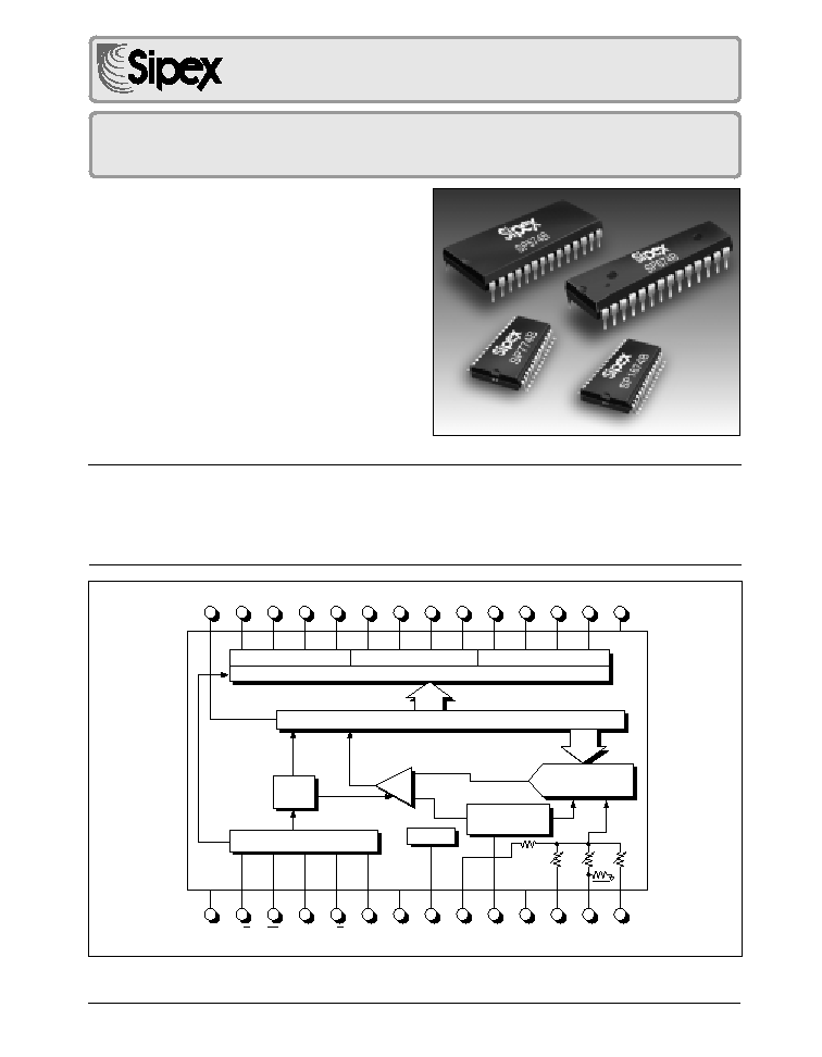
CIRCUIT OPERATION...
The SPx74B are complete monolithic capacitor
DAC≠based 12≠bit analog-to-digital convert-
ers with integral voltage reference, comparator,
successive≠approximation register (SAR),
sample≠and≠hold, clock, output buffers and
control circuitry. The high level of integration
of the SPx74B Series means they require few
external components.
When the control section of the SPx74B initiates
a conversion command, the clock is enabled and
the successive≠approximation register is reset to
all zeros. Once the conversion cycle begins, it can
not be stopped or restarted and data is not available
from the output buffers. The SAR, timed by the
clock, sequences through the conversion cycle and
returns an end≠of≠convert flag to the control sec-
tion of the ADC. The clock is then disabled by the
control section, the output status goes low, and the
control section is enabled to allow the data to be
read by external command.
The internal SPx74B 12≠bit CDAC is sequenced
by the SAR starting from the MSB to the LSB at
the beginning of the conversion cycle to provide
an output voltage from the CDAC that is equal
to the input signal voltage (which is divided by
the input voltage divider network). The com-
parator determines whether the addition of each
successively≠weighted bit voltage causes the
CDAC output voltage summation to be greater
or less than the input voltage; if the sum is less,
the bit is left on; if more, the bit is turned off.
After testing all the bits, the SAR contains a 12≠
bit binary code which accurately represents the
input signal to within
±
1
/
2
LSB.
The internal reference provides the voltage refer-
ence to the CDAC with excellent stability over
temperature and time. The reference is trimmed
to 10.00 Volts
±
1% and can supply up to 2mA to
an external load in addition to that required to
drive the reference input resistor (1mA) and
offset resistor (1mA) when operating with
±
15V
supplies. If the SPx74B is used with
±
12V
supplies, or if external current must be supplied
over the full temperature range, an external
buffer amplifier is recommended. Any external
load on the SPx74B reference must remain
constant during conversion.
FEATURES...
The SPx74B Series feature standard bipolar
and unipolar input ranges of 10V and 20V. Input
ranges are controlled by a bipolar offset pin and
laser-trimmed for specified linearity, gain and
offset accuracy. Power requirements are +5V
and +12V to +15V with a maximum dissipation
of 150mW at the specified voltages. Conversion
times of 8
µ
s, 10
µ
s, 15
µ
s and 25
µ
s are available,
as are units with 10, 25 or 50ppm/
∞
C tempera-
ture coefficients for flexible matching to spe-
cific application requirements.
The SPx74B Series are available in nine prod-
uct grades for each conversion time. The ≠J
and ≠K models are specified over 0∞C to +
70∞C commercial temperature range; the ≠A
and ≠B models are specified over the ≠40∞C
to +85∞C industrial temperature range; the ≠S
and ≠T models are specified over the ≠55∞C to
+125∞C military temperature range. Package
options include 28≠pin CDIP, 28≠pin plastic
DIP (both narrow and wide), 28-pin PLCC
and 28≠pin SOIC.
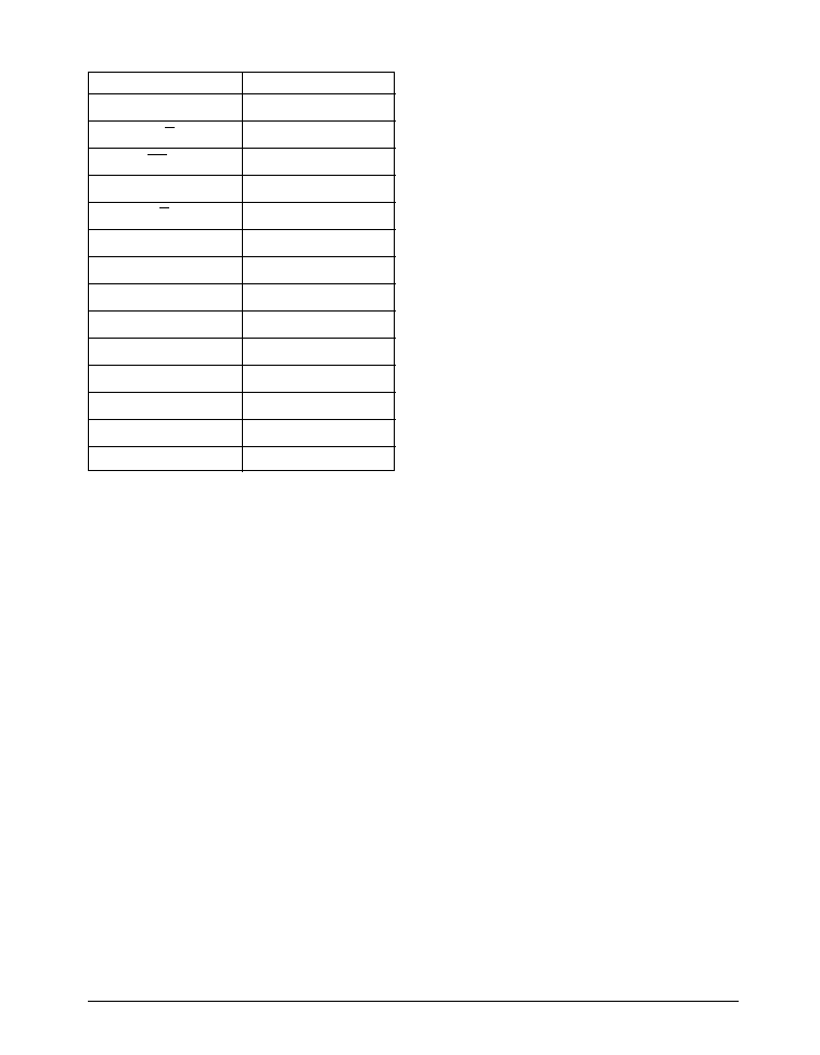
PIN ASSIGNMENTS...
PIN
FUNCTION
PIN
FUNCTION
1
V
LOGIC
28
STS
2
12/8
27
DB
11
(MSB)
3
CS
26
DB
10
4
A
0
25
DB
9
5
R/C
24
DB
8
6
CE
23
DB
7
7
V
CC
22
DB
6
8
REF OUT
21
DB
5
9
ANA GND(AC)
20
DB
4
10
REF IN
19
DB
3
11
N/C*
18
DB
2
12
BIP OFF
17
DB
1
13
10V
IN
16
DB
0
(LSB)
14
20V
IN
15
DIG. GND
*This pin is not connected inside the device so it can
be tied to ≠15V, ground, or left floating.