 | –≠–ª–µ–∫—Ç—Ä–æ–Ω–Ω—ã–π –∫–æ–º–ø–æ–Ω–µ–Ω—Ç: SP239A | –°–∫–∞—á–∞—Ç—å:  PDF PDF  ZIP ZIP |
1
SP30A/234A/235A/236A/237A/238A/239A/
+5V Powered Multi-Channel RS-232 Drivers/Receivers
© Copyright 2000 Sipex Corporation
SP241A/235B/236B/240A/240B/241A/241B
s
Operates from Single +5V Power Supply
(+5V and +12V ≠ SP239A)
s
Meets All RS-232D and V.28 Specifications
s
±
9V Output Swing with +5V Supply
s
Improved Driver Output Capacity for
Mouse Applications
s
Low Power Shutdown ≠ 1
µ
A
s
WakeUp Feature in Shutdown Mode
s
3≠State TTL/CMOS Receiver Outputs
s
±
30V Receiver Input Levels
s
Low Power CMOS ≠ 5mA Operation
s
Wide Charge Pump Capacitor Value
Range ≠ 1-10
µ
F
DESCRIPTION...
The SP230A Series are multi≠channel RS-232 line drivers/receivers that provide a variety of
configurations to fit most communication needs, especially where
±
12V is not available. Some models
feature a shutdown mode to conserve power in battery-powered systems. Some require no external
components. All, except one model, feature a built-in charge pump voltage converter, allowing them
to operate from a single +5V power supply. All drivers and receivers meet all EIA RS-232D and CCITT
V.28 requirements. The Series is available in plastic and ceramic DIP and SOIC packages.
SELECTION TABLE
No. of
No. of
Power
RS-232
RS-232
External
Low Power
TTL
Wake- No. of
Model
Supplies
Drivers
Rcvrs
Components
Shutdown 3≠State
Up
Pins
SP230A
+5V
5
0
4 Capacitors
Yes
No
No
20
SP234A
+5V
4
0
4 Capacitors
No
No
No
16
SP235A
+5V
5
5
None
Yes
Yes
No
24
SP235B
+5V
5
5
None
Yes
Yes
Yes
24
SP236A
+5V
4
3
4 Capacitors
Yes
Yes
No
24
SP236B
+5V
4
3
4 Capacitors
Yes
Yes
Yes
24
SP237A
+5V
5
3
4 Capacitors
No
No
No
24
SP238A
+5V
4
4
4 Capacitors
No
No
No
24
SP239A
+5V/+8.5 to +13.2V
3
5
2 Capacitors
No
Yes
No
24
SP240A
+5V
5
5
4 Capacitors
Yes
Yes
No
44
SP240B
+5V
5
5
4 Capacitors
Yes
Yes
Yes
44
SP241A
+5V
4
5
4 Capacitors
Yes
Yes
No
28
SP241B
+5V
4
5
4 Capacitors
Yes
Yes
Yes
28
Æ
SP230A/234A/235A/236A/237A/238A/239A/241A
SP235B/236B/240A/240B/241A/241B
+5V Powered Multi-Channel RS-232 Drivers/Receivers
SP30A/234A/235A/236A/237A/238A/239A/
+5V Powered Multi-Channel RS-232 Drivers/Receivers
© Copyright 2000 Sipex Corporation
SP241A/235B/236B/240A/240B/241A/241B
2
ABSOLUTE MAXIMUM RATINGS
This is a stress rating only and functional operation of the device at
these or any other conditions above those indicated in the operation
sections of this specification is not implied. Exposure to absolute
maximum rating conditions for extended periods of time may affect
reliability.
V
CC
...............................................................................................................................................................
+6V
V
+
...................................................................................................................
(Vcc≠0.3V) to +13.2V
V
≠
.............................................................................................................................................................
13.2V
Input Voltages:
T
IN
.......................................................................................................................
≠0.3 to (Vcc +0.3V)
R
IN
............................................................................................................................................................
±
30V
Output Voltages:
T
OUT
.................................................................................................
(V+, +0.3V) to (V≠, ≠0.3V)
R
OUT
..............................................................................................................
≠0.3V to (Vcc +0.3V)
Short Circuit Duration:
T
OUT
.........................................................................................................................................
Continuous
Power Dissipation:
CERDIP .............................................................................. 675mW
(derate 9.5mW/
∞
C above +70
∞
C)
Plastic DIP .......................................................................... 375mW
(derate 7mW/
∞
C above +70
∞
C)
Small Outline ...................................................................... 375mW
(derate 7mW/
∞
C above +70
∞
C)
SPECIFICATIONS
All units Vcc=+5V
±
10%; except SP235A/B, Vcc=+5V
±
5%; SP239A only, V+ = +8.5 to +13.2V; All specifications T
MIN
to T
MAX
unless otherwise noted.
PARAMETERS
MIN.
TYP.
MAX.
UNITS
CONDITIONS
POWER REQUIREMENTS
Vcc Power Supply Current
5
10
mA
No load, T
A
= +25
∞
C
SP239A only
0.4
1.0
mA
V+ Power Supply Current
SP239A only
8
15
mA
No load, V
+
= 12V
Shutdown Supply Current
1
10
µ
A
T
A
= +25
∞
C
LOGIC INPUTS
Input Logic Threshold
Low
0.8
Volts
T
IN
; EN, SD
High
2.0
Volts
T
IN
; EN, SD
Logic Pullup Current
15
200
µ
A
T
IN
= 0V
RS-232 INPUTS
RS-232 Input Voltage Range
-30
+30
Volts
RS-232 Input Threshold
Low
0.8
1.2
Volts
Vcc = 5V, T
A
= +25
∞
C
High
1.7
2.4
Volts
Vcc = 5V, T
A
= +25
∞
C
RS-232 Input Hysteresis
0.2
0.5
1.0
Volts
Vcc = 5V
RS-232 Input Resistance
3
5
7
kOhms
T
A
= +25
∞
C, -15V
V
IN
+15V
LOGIC OUTPUTS
Output Voltage
Low
0.4
Volts
I
OUT
= 3.2mA
High
3.5
Volts
I
OUT
= 1.0mA
Output Leakage Current
0.05
±
10
µ
A
EN = V
CC
, 0V
V
OUT
Vcc
RS-232 OUTPUTS
Output Enable Time
400
ns
SP235A/B, SP236A/B,
SP239A & SP241A/B
Output Disable Time
250
ns
SP235A/B, SP236A/B,
SP239A & SP241A/B
Propagation Delay
1.5
µ
s
RS232 to TTL
Instantaneous Slew Rate
30
V/
µ
s
C
L
= 10pF, R
L
= 3≠7k
;
T
A
= +25
∞
C
RS-232 OUTPUTS
Transition Region Slew Rate
3
V/
µ
s
C
L
= 2500pF, R
L
= 3k
;
measured from +3V to -3V or
-3V to +3V
Output Voltage Swing
±
5
±
9
Volts
All transmitter outputs loaded
with 3k
to Ground
Output Resistance
300
Ohms
V
CC
= 0V; V
OUT
=
±
2V
RS-232 Output Short Circuit Current
±
10
mA
Infinite duration

3
SP30A/234A/235A/236A/237A/238A/239A/
+5V Powered Multi-Channel RS-232 Drivers/Receivers
© Copyright 2000 Sipex Corporation
SP241A/235B/236B/240A/240B/241A/241B
0V
5V
0V
5V
0V
0V
T
IN
T
IN
T
OUT
T
OUT
R
L
= 3k
, C
L
= 2,500pF
No load
Transmitter Propagation Delay
Transmitter Output Waveforms
Receiver Output Waveform
Shutdown to V+, V≠ Rise Time
In
Out
5V
0V
0V
SD
V
+
V
≠
Rise Time
R
L
= 3k
; C
L
= 2,500pF
All inputs = 20kHz
T
IN
T
OUT
T
IN
T
OUT
Fall Time
R
L
= 3k
; C
L
= 2,500pF
SP30A/234A/235A/236A/237A/238A/239A/
+5V Powered Multi-Channel RS-232 Drivers/Receivers
© Copyright 2000 Sipex Corporation
SP241A/235B/236B/240A/240B/241A/241B
4
Receiver Propagation Delay
R
IN
5V
0V
R
OUT
5V
0V
R
IN
5V
0V
R
OUT
PINOUT
1
2
3
4
5
6
7
8
9
10
20
19
18
17
16
15
14
13
12
11
SP230A
T OUT
T IN
NC
SD
T OUT
T IN
T IN
V-
C -
C +
4
5
5
4
3
2
2
T OUT
T OUT
T OUT
T IN
T IN
GND
V
C +
V+
C -
3
1
CC
2
1
1
1
2
1
2
3
4
5
6
7
8
16
15
14
13
12
11
10
9
SP234A
T OUT
T OUT
T IN
T IN
V-
C -
C +
C -
3
4
2
2
1
T OUT
T OUT
T IN
T IN
GND
V
C +
V+
1
2
CC
1
2
1
3
4
R IN
R OUT
T IN
SD
EN
T OUT
R IN
R OUT
T IN
T IN
R OUT
R IN
3
5
4
T OUT
T OUT
T OUT
T OUT
R IN
R OUT
T IN
T IN
R OUT
R IN
GND
V
4
3
CC
2
1
1
4
5
2
2
2
1
1
3
3
4
5
5
1
2
3
4
5
6
7
8
9
10
11
12
24
23
22
21
20
19
18
17
16
15
14
13
SP235B
T OUT
R IN
R OUT
SD
EN
T IN
T IN
R OUT
R IN
V-
C -
C +
T OUT
T OUT
T OUT
R IN
R OUT
T IN
T IN
GND
V
C +
V+
C -
4
3
CC
1
2
2
1
1
2
3
4
2
2
1
2
3
4
5
6
7
8
9
10
11
12
24
23
22
21
20
19
18
17
16
15
14
13
SP236B
1
1
1
2
3
3
R IN
R OUT
T IN
SD
EN
T OUT
R IN
R OUT
T IN
T IN
R OUT
R IN
3
5
4
T OUT
T OUT
T OUT
T OUT
R IN
R OUT
T IN
T IN
R OUT
R IN
GND
V
4
3
CC
2
1
1
4
5
2
2
2
1
1
3
3
4
5
5
1
2
3
4
5
6
7
8
9
10
11
12
24
23
22
21
20
19
18
17
16
15
14
13
SP235A
T OUT
R IN
R OUT
SD
EN
T IN
T IN
R OUT
R IN
V-
C -
C +
T OUT
T OUT
T OUT
R IN
R OUT
T IN
T IN
GND
V
C +
V+
C -
4
3
CC
1
2
2
1
1
2
3
4
2
2
1
2
3
4
5
6
7
8
9
10
11
12
24
23
22
21
20
19
18
17
16
15
14
13
SP236A
1
1
1
2
3
3
Fall Time
Rise Time

5
SP30A/234A/235A/236A/237A/238A/239A/
+5V Powered Multi-Channel RS-232 Drivers/Receivers
© Copyright 2000 Sipex Corporation
SP241A/235B/236B/240A/240B/241A/241B
Receiver Output Enable/Disable Times
Disable
5V
0V
5V
0V
EN IN
R
OUT
Enable
5V
0V
5V
0V
EN IN
R
OUT
PINOUT
T OUT
R IN
R OUT
T IN
T OUT
T IN
T IN
R OUT
R IN
V-
C -
C +
T OUT
T OUT
R IN
R OUT
T IN
R OUT
R IN
GND
V
C +
V+
C -
3
2
CC
1
2
1
1
1
3
2
3
2
2
1
2
3
4
5
6
7
8
9
10
11
12
24
23
22
21
20
19
18
17
16
15
14
13
SP238A
2
1
1
4
4
4
3
4
T IN
T IN
R OUT
R IN
T OUT
T OUT
R IN
R OUT
T IN
No Connection
EN
T OUT
R OUT
R 1N
GND
V
V+
C+
C-
V-
R IN
R OUT
R OUT
R IN
1
1
CC
1
2
4
2
5
5
3
1
2
3
4
5
6
7
8
9
10
11
12
24
23
22
21
20
19
18
17
16
15
14
13
SP239A
2
2
1
3
4
3
3
T OUT
R IN
R OUT
T IN
T OUT
T IN
T IN
R OUT
R IN
V-
C -
C +
T OUT
T OUT
T OUT
R IN
R OUT
T IN
T IN
GND
V
C +
V+
C -
4
3
CC
1
2
2
1
1
2
3
4
2
2
1
2
3
4
5
6
7
8
9
10
11
12
24
23
22
21
20
19
18
17
16
15
14
13
SP237A
1
1
1
5
3
3
2
5
T OUT
R IN
R OUT
SHUTDOWN (SD)
EN
R IN
R OUT
T IN
T IN
R OUT
R IN
V-
C -
C +
T OUT
T OUT
T OUT
R IN
R OUT
T IN
T IN
R OUT
R IN
GND
V
C +
V+
C -
1
1
CC
1
2
4
2
5
3
SP241B
2
2
3
4
3
1
2
3
4
5
6
7
8
9
10
11
12
13
14
28
27
26
25
24
23
22
21
20
19
18
17
16
15
1
1
1
2
2
5
3
4
4
T OUT
R IN
R OUT
SHUTDOWN (SD)
EN
R IN
R OUT
T IN
T IN
R OUT
R IN
V-
C -
C +
T OUT
T OUT
T OUT
R IN
R OUT
T IN
T IN
R OUT
R IN
GND
V
C +
V+
C -
1
1
CC
1
2
4
2
5
3
SP241B
2
2
3
4
3
1
2
3
4
5
6
7
8
9
10
11
12
13
14
28
27
26
25
24
23
22
21
20
19
18
17
16
15
1
1
1
2
2
5
3
4
4
N.C.
N.C.
N.C.
V≠
C
2
≠
C
2
+
C
1
≠
V+
C
1
+
N.C.
N.C.
N.C.
T
5
IN
R
3
OUT
R
3
IN
T
4
OUT
T
3
OUT
T
1
OUT
T
2
OUT
N.C.
R
2
IN
N.C.
N.C.
SHUTDOWN
EN
T
5
OUT
R
4
IN
R
4
OUT
T
4
IN
T
3
IN
R
5
OUT
R
5
IN
N.C.
N.C.
R
2
OUT
T
2
IN
T
1
IN
R
1
OUT
R
1
IN
GND
V
CC
N.C.
N.C.
N.C.
SP240A/B
1
2
3
4
5
6
7
8
9
10
11
12
13
14
15
16
17
18
19
20
21
22
44
43
42
41
40
39
38
37
36
35
34
33
32
31
30
29
28
27
26
25
24
23
SP30A/234A/235A/236A/237A/238A/239A/
+5V Powered Multi-Channel RS-232 Drivers/Receivers
© Copyright 2000 Sipex Corporation
SP241A/235B/236B/240A/240B/241A/241B
6
FEATURES...
The multi≠channel RS-232 line drivers/receivers pro-
vides a variety of configurations to fit most communi-
cation needs, especially those applications where
±
12V is not available. The SP230A, SP235A/B,
SP236A/B, SP240A/B, and SP241A/B feature a
shutdown mode which reduces device power dissipa-
tion to less than 5
µ
W. All feature low power CMOS
operation, which is particularly beneficial in battery-
powered systems. The SP235A/B use no external
components and are ideally suited where printed
circuit board space is limited.
All products in the Series, except the SP239A, include
two charge pump voltage converters which allow
them to operate from a single +5V supply. These
converters convert the +5V input power to the
±
10V needed to generate the RS-232 output levels.
The SP239A is designed to operate from +5V and
+12V supplies. An internal charge pump converter
produces the necessary ≠12V supply. All drivers
and receivers meet all EIA RS-232D and CCITT
V.28 specifications.
The Series are available for use over the commer-
cial, industrial and military temperature ranges.
They are packaged in plastic and ceramic DIP, and
SOIC packages. For product processed and
screened to MIL≠M≠38510 and MIL≠STD≠883C
requirements, please consult the factory.
THEORY OF OPERATION
The SP230A/B≠241A/B series devices are made up
of three basic circuit blocks ≠ 1) transmitter, 2) receiver
and 3) charge pump. Each model within the series
incorporates variations of these circuits to achieve the
desired configuration and performance.
Driver/Transmitter
The drivers are inverting transmitters, which accept
TTL or CMOS inputs and output the RS-232 signals
with an inverted sense relative to the input logic levels.
Typically the RS-232 output voltage swing is
±
9V.
Even under worst-case loading conditions of 3k
and
2500pF, the output is guaranteed to be
±
5V, which is
consistent with the RS-232 standard specifications.
The transmitter outputs are protected against infi-
nite short-circuits to ground without degradation
in reliability.
The drivers of the SP230A, SP235A/B, SP236A/B,
SP240A/B and SP241A/B can be tri-stated by using
the SHUTDOWN function. In this "power-off" state,
the output impedance will remain greater than 300
Ohms, again satisfying the RS-232 specifications.
Should the input of the driver be left open, an internal
400k
pull≠up resistor to V
CC
forces the input high,
thus committing the output to a low state.
The slew rate of the transmitter output is internally
limited to a maximum of 30V/
µ
s in order to meet the
Table 1. EIA Standards Definition
20kbps
100kbps
10Mbps
10Mbps
64kbps
7
SP30A/234A/235A/236A/237A/238A/239A/
+5V Powered Multi-Channel RS-232 Drivers/Receivers
© Copyright 2000 Sipex Corporation
SP241A/235B/236B/240A/240B/241A/241B
standards [EIA RS-232≠D 2.1.7, Paragraph (5)]. The
transition of the loaded output from V
OL
to V
OH
clearly
meets the monotonicity requirements of the standard
[EIA RS-232≠D 2.1.7, Paragraphs (1) & (2)].
Receivers
The receivers convert RS-232 input signals to in-
verted TTL signals. Since the input is usually from a
transmission line, where long cable lengths and sys-
tem interference can degrade the signal, the inputs
have a typical hysteresis margin of 500mV. This
ensures that the receiver is virtually immune to
noisy transmission lines.
The input thresholds are 0.8V minimum and 2.4V
maximum, again well within the
±
3V RS-232 re-
quirements. The receiver inputs are also protected
against voltages up to
±
30V. Should an input be left
unconnected, a 5k
pulldown resistor to ground will
commit the output of the receiver to a high state.
In actual system applications, it is quite possible for
signals to be applied to the receiver inputs before
power is applied to the receiver circuitry. This occurs,
for example, when a PC user attempts to print, only to
realize the printer wasn't turned on. In this case an
RS-232 signal from the PC will appear on the receiver
input at the printer. When the printer power is turned
on, the receiver will operate normally. All series
devices are fully protected. Again, to facilitate use in
"real-world" applications, the receiver outputs can be
tri≠stated by bringing the ENABLE (EN) pin high,
with the driver remaining full active.
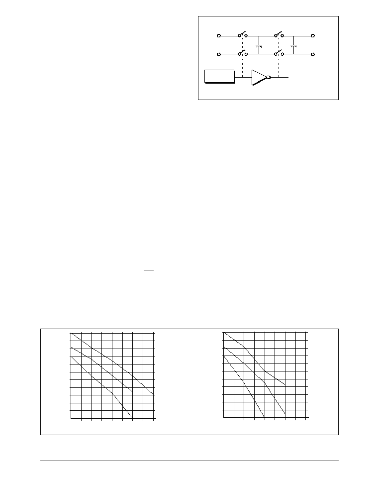
Charge Pump
The charge pump section of the SP230A series allows
the circuit to operate from a single +5V,
±
10% power
S1
GND
V
CC
+
V+ = 2V
CC
+
V
CC
S2
S3
S4
C1
C3
INTERNAL
OSCILLATOR
Figure 1. Charge Pump Voltage Doubler
supply by generating the required operating voltages
internal to the devices. The charge pump consists of
two sections -- 1) a voltage doubler and 2) a voltage
inverter.
As shown in Figure 1, an internal oscillator
triggers the charge accumulation and voltage
inversion. The voltage doubler momentarily
stores a charge on capacitor C
1
equal to V
CC
,
reference to ground. During the next transition
of the oscillator this charge is boot≠strapped to
transfer charge to capacitor C
3
. The voltage
across C
3
is now from V
CC
to V
+
.
In the inverter section (Figure 2), the voltage
across C
3
is transferred to C
2
forcing a range of
0V to V
+
across C
2
. Boot≠strapping of C
2
will
then transfer charge to C
4
to generate V
-
.
The values of the capacitors are somewhat
non-critical and can be varied, however the
performance will be affected. As C
3
and C
4
are
reduced, higher levels of ripple will appear.
Lower values of C
1
and C
2
will increase the
10.5
10.0
9.5
9.0
8.5
8.0
7.5
7.0
6.5
6.0
5.5
5.0
V- (Abs.)
0
5
10
15
20
25
30
35
40
V- I (mA)
OUT
V =5.5V
CC
V =5V
CC
V =4.5V
CC
10.5
10.0
9.5
9.0
8.5
8.0
7.5
7.0
6.5
6.0
5.5
5.0
V+ (Abs.)
0
5
10
15
20
25
30
35
40
V+ I (mA)
OUT
V =5.5V
CC
V =5V
CC
V =4.5V
CC
Charge Pump Output Loading versus VCC; a) V
+
; b) V
≠
a)
b)
SP30A/234A/235A/236A/237A/238A/239A/
+5V Powered Multi-Channel RS-232 Drivers/Receivers
© Copyright 2000 Sipex Corporation
SP241A/235B/236B/240A/240B/241A/241B
8
ENABLE Input (EN)
The SP235A/B, SP236A/B, SP239A, SP240A/
B, and SP241A/B all feature an enable input
(EN), which allows the receiver outputs to be
either tri≠stated or enabled. The enable input is
active low; 0V applied to EN will enable the
receiver outputs. This can be especially useful
when the receiver is tied directly to a micropro-
cessor data bus.
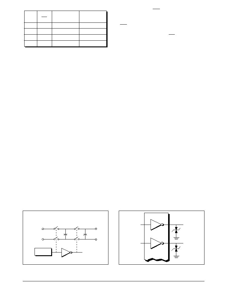
Protection From Shorts to >
±
15V
The driver outputs are protected against shorts
to ground, other driver outputs, and V
+
or V
-
.
For protection against voltages exceeding
±
15V,
two back≠to≠back zener diodes connected to
clamp the outputs to an acceptable voltage level
are recommended. (Refer to Figure 3.)
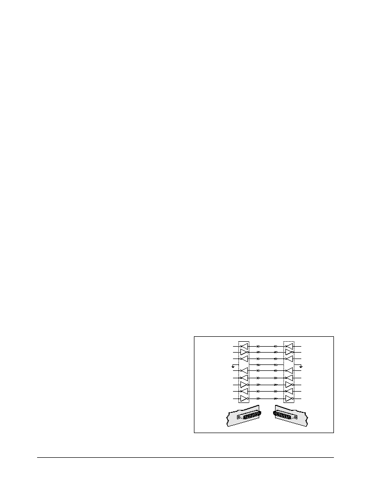
Improved Drive Capability for Mouse
Applications
Each of the devices in this data sheet have
improved drive capability for non-standard ap-
plications. Although the EIA RS-232D stan-
dards specify the maximum loading to be 3k
and 2500pF, the SP230A, SP234A, SP235A/B,
SP236A/B, SP237A, SP238A, SP239, SP240A/
B, and SP241A/B can typically drive loads as
low as 1k
and still maintain
±
5V outputs. This
feature is especially useful when the serial port
is intended to be used for a "self-powered"
mouse. In this case the voltage necessary to
operate the circuits in the mouse can be derived
from the RS-232 driver output as long as the
loading is
1k
(refer to Figure 4). For applica-
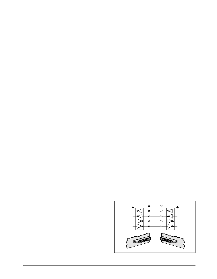
tions which even exceed this requirement, driv-
ers can be connected in parallel, increasing the
drive capability to 750
, while maintaining the
±
5V V
OH
and V
OL
levels (refer to Figure 5).
SD
EN
Power
Up/Down
Receiver
Outputs
0
0
1
1
0
1
0
1
Up
Up
Down
Down
Enable
Tri≠state
Enable
Tri≠state
Figure 3. High Voltage Short Circuit Protection
Figure 2. Charge Pump Voltage Inverter
T IN
1
T IN
T OUT
T OUT
2
1
2
15V ZENER
15V ZENER
S1
FROM
VOLTAGE DOUBLER
V+
+
V- = -(V+)
+
S2
S3
S4
C2
C4
INTERNAL
OSCILLATOR
GND
GND
output impedance of V
+
and V
-
, which will
degrade V
OH
and V
OL
. Capacitor values can be
as low as 1.0
µ
F.
Shutdown (SD)
The SP230A, SP235A/B, SP236A/B,
SP240A/B and SP241A/B all feature a control
input which will disable the part and reduce V
CC
current typically to less than 5
µ
A, which is
especially useful to designers of battery≠pow-
ered systems. In the "power≠off" mode the
receiver and transmitter will both be tri-stated.
V
+
will discharge to V
CC
, and V
-
will discharge
to ground.
For complete shutdown to occur and the 10
µ
A
current drain to be realized, the following con-
ditions must be met:
∑ +5.00V must be applied to the SD pin;
∑ ENABLE must either 0V, +5.0V or not connected;
∑ the transmitter inputs must be either +5.0V or not
connected;
∑ V
CC
must be +5V;
∑ Receiver inputs must be >0V and <+5V
Please note that for proper operation, the SD
input pin must never be left floating.
Table 2. Wake≠Up Truth Table

9
SP30A/234A/235A/236A/237A/238A/239A/
+5V Powered Multi-Channel RS-232 Drivers/Receivers
© Copyright 2000 Sipex Corporation
SP241A/235B/236B/240A/240B/241A/241B
Figure 4. Mouse Application Drive Capability
10
9
8
7
6
5
4
3
2
1
0
V
OL/
V
OH
(Volts)
0
2
4
6
8
10
12
18
20
I
OL
/I
OH
(mA)
16
14
22
V
OL
vs I
OL
V
OH
vs I
OH
Figure 5. Parallel Drivers
T IN
T OUT
Wake-Up Feature
The SP235B, SP236B, SP240B and SP241B
have a wake-up feature that keeps all receivers
in an enabled state when the device is in the
shutdown mode. Table 2 defines the truth table
for the wake-up function. Timing for the wake-up
function is shown in Figure 6.
If the SP235B, SP236B, SP240B and SP241B
are powered up in the shutdown state (SD driven
high during V
CC
power up), the part must remain
in a powered on state for a minimum of 3ms
before the wake-up function can be used. After
the 3ms wait time, there is a 2ms delay time
before data is valid for both enable and disable
+5V
0V
+5V
0V
R
OUT
SD
POWER-UP WITH SD HIGH (charge pump section in shutdown state)
+5V
0V
+5V
0V
R
OUT
SD
POWER-UP WITH SD LOW (charge pump section in active mode)
t
WAIT
t
ENABLE
t
0
(power up)
t
0
(power up)
+5V
0V
+5V
0V
R
OUT
SD
EXERCISING WAKE≠UP FEATURE
t
0
(power up)
DATA
VALID
t
WAIT
DATA
VALID
DATA
VALID
DATA
VALID
DATA
VALID
t
ENABLE
t
ENABLE
t
ENABLE
SPECIFICATIONS:
(V
CC
=+5V±10%, T
A
=25∞C)
PARAMETER MIN. TYP. MAX.
t
WAIT
2ms 3ms
t
ENABLE
1ms 2ms
Figure 6. Wake≠Up and Shutdown Timing
SP30A/234A/235A/236A/237A/238A/239A/
+5V Powered Multi-Channel RS-232 Drivers/Receivers
© Copyright 2000 Sipex Corporation
SP241A/235B/236B/240A/240B/241A/241B
10
of the charge pump. If the SP2XXB is powered
up with SD low, then only the 2ms delay time
will apply (refer to Figure 6). Under normal
operation, both the wait time and delay time
should be transparent to the user.
With only the receivers activated, the device
typically draws less than 5
µ
A (10
µ
A max) sup-
ply current. In the case of a modem interfaced to
a computer in power-down mode, the RI (ring
indicator) signal from the modem would be used
to "wake up" the computer, allowing it to accept
the data transmission.
After the ring indicator signal has propagated
through the SP2XXB receiver, it can be used to
trigger the power management circuitry of the
computer to power up the microprocessor and
bring the SD pin to the SP2XXB low, taking it
out of shutdown. The receiver propagation de-
lay is typically 1
µ
s. The enable time for V+ and
V- is typically 2ms. After V+ and V- have
settled to their final values, a signal can be sent
back to the modem on the DTR (Data Terminal
Ready) pin signifying that the computer is ready
to accept and transmit data.
All receivers that are active during shutdown
maintain 500mV (typ.) of hysteresis.
Varying Capacitor Values
As stated earlier, the capacitor values are some-
what non-critical. Since they are an actual compo-
nent of the charge pump circuitry, their value will
affect its performance, which in turn affects the
V
OH
and V
OL
levels. There is no upper limit for the
value of any of the four capacitors; lower values
will impact performance. C
1
and C
2
are respon-
sible for the charge accumulation and can be
reduced to 1
µ
F; this will increase the output im-
pedance of V
+
and V
≠
. Reducing these capacitor
values will limit the ability of the SP2XXA/B to
maintain the dc voltages needed to generate the
RS-232 output levels. Capacitors C
3
and C
4
can
also be reduced to 1
µ
F; doing so will increase the
ripple on V
+
and V≠.
Typically each driver will require 1
µ
F of capaci-
tance as a minimum to operate within all specified
parameters; if five drivers are active in the circuit,
then C
3
and C
4
should be 5
µ
F. In order to operate
at these minimum values, the supply voltage must
be maintained at +5.0V
±
5%. Also, the ambient
operating temperature must be less than 60
∞
C.
The capacitor values must be chosen to suit the
particular application. The designer must bal-
ance board space, cost and performance to maxi-
mize the design. The capacitors can be polarized
or non≠polarized, axial-leaded or surface-mount.
As the size and value decrease, so does the cost;
however, the value should be chosen to accom-
modate worst-case load conditions.
IBM Modem Port Interconnections
Computer
D
R
D
R
R
D
R
D
Transmitted Data
(To Be Printed)
Ready To Send
Clear To Send
Data Set Ready
Signal Ground
4
2
5
6
7
Received Data
(To Be Printed)
Ready To Send
Clear To Send
Data Set Ready
Signal Ground
Modem
R
D
Received Data
3
Received Data
R
D
Data Carrier Detect
8
Data Carrier Detect
D
R
Data Terminal Ready
20
Data Terminal Ready
R
D
Ring Indicator
22
Ring Indicator
SP239A
SP237A
INTERFACE EXAMPLE ≠ A MODEM
ON THE IBM PC SERIAL PORT
The RS-232 standard defines 22 serial interface
signals. These signals consist of ground lines,
timing, data, control and test signals, plus a set
of signals rarely used for a second data channel.
Many of these signal lines are not used in typical
RS-232 applications; in fact, the IBM
Æ
PC serial
port is implemented using only nine pins.
For example, consider the case of a PC using this
nine pin port to communicate with a peripheral
device such as a modem. We see the following
activity on each of the RS-232 lines as the
computer and modem are activated and commu-
nicate with each other as well as the remote
modem at the other end of the phone line.
Signal Ground (GND)
The Signal Ground pin acts as a reference for all
the other signals. This pin is simply maintained
at a 0V level to serve as a level to which all other
signals are referenced. Both the PC and the
modem will have this line connected to their
respective internal ground lines.
11
SP30A/234A/235A/236A/237A/238A/239A/
+5V Powered Multi-Channel RS-232 Drivers/Receivers
© Copyright 2000 Sipex Corporation
SP241A/235B/236B/240A/240B/241A/241B
Data Terminal Ready (DTR)
This is the pin the computer uses to tell periph-
eral devices that it is on≠line and ready to
communicate.
Data Set Ready (DSR)
Peripheral devices use this line to tell the com-
puter that they are on≠line and ready to commu-
nicate. When the modem is turned on and has
completed its self≠test routine (assuming it does
one), it will send a signal to the PC by asserting
this line.
Request To Send (RTS)
The computer activates this line to notify the
peripheral device that it is ready to send data. In
this example, the computer notifies the modem
that it is ready to send data to be transmitted by
the modem.
Clear To Send (CTS)
This is the line on which the peripheral device
tells the computer that it is ready to receive data
from the computer. If the modem was not ready,
i.e. it was performing a loop≠back self≠test, for
example, it would not assert this line. Once the
modem was ready to receive data from the PC,
it would assert this line. When it receives the
CTS signal from the modem, the PC knows that
a data transmission path has been established
between itself and the modem.
Transmitted Data (TD or TX)
This is the pin on which the computer sends the
actual data signal to be transmitted, i.e. a posi-
tive voltage (+3V to +15V) to represent a logic
"0", and a negative voltage (≠3V to ≠15V) to
represent a logic "1". The PC would send the
data on this line to be transmitted by the modem.
Ring Indicator (RI)
This line is used by the peripheral device to tell
the computer that a remote device wants to start
communicating. The modem would activate the
RI line to tell the computer that the remote
modem was calling, i.e. the phone is ringing.
Data Carrier Detect (DCD)
This line is used by the modem to tell the
computer that it has completed a transmission
path with the remote modem, and to expect to
start receiving data at any time.
Received Data (RD or RX)
This is the pin on which the modem sends the
computer the incoming data signal, i.e. a posi-
tive voltage (+3V to +15V) to represent a logic
"0", and a negative voltage (-3V to -15V) to
represent a logic "1".
INTERFACE EXAMPLE ≠ A PRINTER
ON THE IBM PC SERIAL PORT
The RS-232 standard defines 22 serial interface
signals. These signals consist of ground lines,
timing, data, control and test signals, plus a set of
signals rarely used for a second data channel.
Many of these signal lines are not used in typical
RS-232 applications; in fact, the IBM
Æ
PC serial
port is implemented using only nine pins.
For example, consider the case of a PC using this
nine pin port to communicate with a peripheral
device such as a printer. We see the following
activity on each of the RS-232 lines as the com-
puter and printer are activated and communicate.
Signal Ground (GND)
The Signal Ground pin acts as a reference for all the
other signals. This pin is simply maintained at a 0V
level to serve as a level to which all other signals
are referenced. Both the PC and the printer will
have this line connected to their respective internal
ground lines.
Data Terminal Ready (DTR)
This is the pin the computer uses to tell peripheral
devices that it is on≠line and ready to communi-
Computer
D
R
D
R
R
D
R
D
Transmitted Data
(To Be Printed)
Ready To Send
Clear To Send
Data Set Ready
Signal Ground
4
2
5
6
7
Received Data
(To Be Printed)
Ready To Send
Clear To Send
Data Set Ready
Signal Ground
Printer
SP231A/232A
SP231A/232A
IBM Printer Port Interconnections

SP30A/234A/235A/236A/237A/238A/239A/
+5V Powered Multi-Channel RS-232 Drivers/Receivers
© Copyright 2000 Sipex Corporation
SP241A/235B/236B/240A/240B/241A/241B
12
cate. Once the computer is powered≠up and ready,
it will send out a signal on the DTR to inform the
printer that it is powered≠up and ready to go. The
printer really doesn't care, since it will simply print
data as it is received. Accordingly, this pin is not
needed at the printer.
Data Set Ready (DSR)
Peripheral devices use this line to tell the computer
that they are on≠line and ready to communicate.
When the printer is turned on and has completed its
self≠test routine (assuming it does one), it will send
a signal to the PC by asserting this line.
Request To Send (RTS)
The computer activates this line to notify the
peripheral device that it is ready to send data. In this
example, the computer notifies the printer that it is
ready to send data to be printed by the printer.
Clear To Send (CTS)
This is the line on which the peripheral device tells
the computer that it is ready to receive data from
the computer. If the printer was not ready, i.e. it
was out of paper, for example, it would not assert
this line. Once the printer was ready to receive data
from the PC, it would assert this line. When it
receives the CTS signal from the printer, the PC
knows that a data transmission path has been
established between itself and the printer.
Transmitted Data (TD or TX)
This is the pin on which the computer sends the
actual data signal representing the actual informa-
tion to be printed, i.e. a positive voltage (+3V to
+15V) to represent a logic "0", and a negative
voltage (-3V to -15V) to represent a logic "1".
Ring Indicator (RI)
This line is used by the peripheral device to tell the
computer that a remote device wants to start com-
municating. A modem would activate the RI line
to tell the computer that a remote modem was
calling, i.e. the phone is ringing. In the case of a
printer, this line is unused.
Data Carrier Detect (DCD)
This line is used by a peripheral device to tell the
computer to expect to start receiving data at any
time. Since the printer would not be sending data
to the PC in this case this line is not needed.
Received Data (RD or RX)
This is the pin on which the computer receives the
incoming data signal, i.e. a positive voltage (+3V
to +15V) to represent a logic "0", and a negative
voltage (-3V to -15V) to represent a logic "1".
Again, in this instance, since the printer will not be
sending the PC any data, this line is not needed.
13
SP30A/234A/235A/236A/237A/238A/239A/
+5V Powered Multi-Channel RS-232 Drivers/Receivers
© Copyright 2000 Sipex Corporation
SP241A/235B/236B/240A/240B/241A/241B
235A
11
GND
T
4
16
1
4
4
T
3
15
2
3
3
T
2
7
4
2
2
T
1
8
3
T IN
1
T OUT
1
400k
400k
400k
400k
TTL/CMOS INPUTS
RS-232 OUTPUTS
12
V
CC
+5V INPUT
T IN
T IN
T IN
T OUT
T OUT
T OUT
T
5
22
19
5
5
400k
T IN
T OUT
R
2
6
5
R IN
R OUT
2
R
1
9
10
R IN
R OUT
1
2
1
5k
5k
R
4
17
18
R IN
R OUT
4
R
3
23
24
R IN
R OUT
3
4
3
5k
5k
R
5
14
13
R IN
R OUT
5
5
5k
TTL/CMOS OUTPUTS
RS-232 INPUTS
SD
21
EN
20
235B
230A
234A
T
4
14
15
4
4
T
3
13
16
3
3
T
2
3
2
2
2
T
1
4
1
T IN
1
T OUT
1
5
GND
400k
400k
400k
400k
TTL/CMOS INPUTS
RS-232 OUTPUTS
11
10
9
7
C +
C -
C +
C -
2
2
1
1
12
6
V
CC
V+
+
+
+
+
1≠10µF
16V
1≠10µF
16V
1≠10µF
6.3V
+5V to +10V
Voltage Doubler
+10V to -10V
Voltage Inverter
+5V INPUT
8
T IN
T IN
T IN
T OUT
T OUT
T OUT
V-
1≠10µF
6.3V
11
GND
T
4
16
1
4
4
T
3
15
2
3
3
T
2
7
4
2
2
T
1
8
3
T IN
1
T OUT
1
400k
400k
400k
400k
TTL/CMOS INPUTS
RS-232 OUTPUTS
12
V
CC
+5V INPUT
T IN
T IN
T IN
T OUT
T OUT
T OUT
T
5
22
19
5
5
400k
T IN
T OUT
R
2
6
5
R IN
R OUT
2
R
1
9
10
R IN
R OUT
1
2
1
5k
5k
R
4
17
18
R IN
R OUT
4
R
3
23
24
R IN
R OUT
3
4
3
5k
5k
R
5
14
13
R IN
R OUT
5
5
5k
TTL/CMOS OUTPUTS
RS-232 INPUTS
SD
21
EN
20
TYPICAL CIRCUITS
T
5
19
16
5
T OUT
5
T
4
15
20
4
T OUT
4
T
3
14
1
3
3
T
2
4
3
2
2
T
1
5
2
T IN
1
1
6
18
17
SD
NC
GND
400k
400k
400k
400k
400k
TTL/CMOS INPUTS
RS-232 OUTPUTS
12
11
10
8
C +
C -
C +
C -
2
2
1
1
13
1≠10µF
6.3V
7
V
CC
V+
+
+
+
+
1≠10µF
16V
1≠10µF
16V
1≠10µF
6.3V
+5V to +10V
Voltage Doubler
+10V to -10V
Voltage Inverter
+5V INPUT
9
T IN
T IN
T IN
T IN
T OUT
T OUT
T OUT
V-
SP30A/234A/235A/236A/237A/238A/239A/
+5V Powered Multi-Channel RS-232 Drivers/Receivers
© Copyright 2000 Sipex Corporation
SP241A/235B/236B/240A/240B/241A/241B
14
237A
238A
236A
236B
TYPICAL CIRCUITS
8
14
13
12
10
C +
C -
C +
C -
2
2
1
1
15
9
V
CC
V+
+
+
+
+
1≠10µF
16V
1≠10µF
16V
1≠10µF
6.3V
+5V to +10V
Voltage Doubler
+10V to -10V
Voltage Inverter
+5V INPUT
11
V-
T
4
19
24
4
4
T
3
18
2
3
3
T
2
7
1
2
2
T
1
6
3
T IN
1
T OUT
1
400k
400k
400k
400k
TTL/CMOS INPUTS
RS-232 OUTPUTS
T IN
T IN
T IN
T OUT
T OUT
T OUT
R
2
22
23
R IN
R OUT
2
R
1
5
4
R IN
R OUT
1
2
1
5k
5k
R
3
17
16
R IN
R OUT
3
3
5k
3
TTL/CMOS OUTPUTS
RS-232 INPUTS
SD
21
EN
20
GND
1≠10µF
6.3V
8
14
13
12
10
C +
C -
C +
C -
2
2
1
1
15
9
V
CC
V+
+
+
+
+
1≠10µF
16V
1≠10µF
16V
1≠10µF
6.3V
+5V to +10V
Voltage Doubler
+10V to -10V
Voltage Inverter
+5V INPUT
11
V-
T
4
19
24
4
4
T
3
18
2
3
3
T
2
7
1
2
2
T
1
6
3
T IN
1
T OUT
1
400k
400k
400k
400k
TTL/CMOS INPUTS
RS-232 OUTPUTS
T IN
T IN
T IN
T OUT
T OUT
T OUT
R
2
22
23
R IN
R OUT
2
R
1
5
4
R IN
R OUT
1
2
1
5k
5k
R
3
17
16
R IN
R OUT
3
3
5k
TTL/CMOS OUTPUTS
RS-232 INPUTS
GND
T
5
21
20
5
5
400k
T IN
T OUT
1≠10µF
6.3V
8
14
13
12
10
C +
C -
C +
C -
2
2
1
1
15
9
V
CC
V+
+
+
+
+
1≠10µF
16V
1≠10µF
16V
1≠10µF
6.3V
+5V to +10V
Voltage Doubler
+10V to -10V
Voltage Inverter
+5V INPUT
11
V-
T
4
19
24
4
4
T
3
18
2
3
3
T
2
1
2
2
T
1
5
T IN
1
T OUT
1
400k
400k
400k
400k
TTL/CMOS INPUTS
RS-232 OUTPUTS
T IN
T IN
T IN
T OUT
T OUT
T OUT
R
2
22
3
R IN
R OUT
2
R
1
6
7
R IN
R OUT
1
2
1
5k
5k
R
3
23
R IN
R OUT
3
3
5k
TTL/CMOS OUTPUTS
RS-232 INPUTS
GND
21
20
R
4
17
16
R IN
R OUT
4
4
5k
4
1≠10µF
6.3V
15
SP30A/234A/235A/236A/237A/238A/239A/
+5V Powered Multi-Channel RS-232 Drivers/Receivers
© Copyright 2000 Sipex Corporation
SP241A/235B/236B/240A/240B/241A/241B
3
GND
T
3
16
13
3
3
T
2
23
20
2
2
T
1
24
19
T IN
1
T OUT
1
400k
400k
400k
TTL/CMOS INPUTS
RS-232 OUTPUTS
4
V
CC
+5V INPUT
T IN
T IN
T OUT
T OUT
R
2
22
21
R IN
R OUT
2
R
1
1
2
R IN
R OUT
1
2
1
5k
5k
R
4
17
12
R IN
R OUT
4
R
3
11
18
R IN
R OUT
3
4
3
5k
5k
R
5
10
9
R IN
R OUT
5
5
5k
TTL/CMOS OUTPUTS
RS-232 INPUTS
NC*
15
EN
14
7
6 C+
C-
8
V+
+
+
1≠10µF
16V
+12V to -12V
Voltage Converter
5
V-
1≠10µF
16V
12V _ 10%
+
NC* = No Connection
239A
241B
10
GND
T
3
20
1
3
3
T
2
6
3
2
2
T
1
7
2
T IN
1
T OUT
1
400k
400k
400k
TTL/CMOS INPUTS
RS-232 OUTPUTS
T IN
T IN
T OUT
T OUT
R
2
5
27
R IN
R OUT
2
R
1
8
4
R IN
R OUT
1
2
1
5k
5k
R
4
26
18
R IN
R OUT
4
R
3
22
23
R IN
R OUT
3
4
3
5k
5k
R
5
19
9
R IN
R OUT
5
5
5k
TTL/CMOS OUTPUTS
RS-232 INPUTS
SD
25
EN
24
T
4
21
28
4
4
400k
T IN
T OUT
16
15
14
12
C +
C -
C +
C -
2
2
1
1
17
11
V
CC
V+
+
+
+
+
1≠10µF
16V
1≠10µF
16V
1≠10µF
6.3V
+5V to +10V
Voltage Doubler
+10V to -10V
Voltage Inverter
+5V INPUT
13
V-
1≠10µF
6.3V
241A
240A/B
18
GND
T
3
37
6
3
3
T
2
8
2
2
T
1
7
T IN
1
T OUT
1
400k
400k
400k
TTL/CMOS INPUTS
RS-232 OUTPUTS
T IN
T IN
T OUT
T OUT
13
R IN
R OUT
2
R
1
16
10
R IN
R OUT
1
2
1
R
4
3
35
R IN
R OUT
4
R
3
39
40
R IN
R OUT
3
4
3
R
5
36
17
R IN
R OUT
5
5
TTL/CMOS OUTPUTS
RS-232 INPUTS
SD
43
EN
42
28
27
25
30
19
V
CC
V+
+
+
+
+
10µF
16V
4.7µF
16V
4.7µF
6.3V
+5V to +10V
Voltage Doubler
+10V to -10V
Voltage Inverter
+5V INPUT
26
V-
10µF
6.3V
SP240A/B
14
15
29
4
5k
T
5
2
41
T
4
5
400k
400k
T IN
T IN
T OUT
38
4
5
T OUT
5
4
C +
1
C ≠
1
C +
2
C ≠
2
R
2
5k
5k
5k
5k
TYPICAL CIRCUITS

SP30A/234A/235A/236A/237A/238A/239A/
+5V Powered Multi-Channel RS-232 Drivers/Receivers
© Copyright 2000 Sipex Corporation
SP241A/235B/236B/240A/240B/241A/241B
16
ORDERING INFORMATION
Model ....................................................................................... Temperature Range .................................................................... Package
SP230ACP ..................................................................................... 0
∞
C to +70
∞
C ..................................................................... 20≠pin Plastic DIP
SP230ACT ..................................................................................... 0
∞
C to +70
∞
C .............................................................................. 20≠pin SOIC
SP230ACX ..................................................................................... 0
∞
C to +70
∞
C ............................................................................................ Dice
SP230AEP ................................................................................... ≠40
∞
C to +85
∞
C ................................................................... 20≠pin Plastic DIP
SP230AET ................................................................................... ≠40
∞
C to +85
∞
C ............................................................................ 20≠pin SOIC
SP234ACP ..................................................................................... 0
∞
C to +70
∞
C ..................................................................... 16≠pin Plastic DIP
SP234ACT ..................................................................................... 0
∞
C to +70
∞
C .............................................................................. 16≠pin SOIC
SP234ACX ..................................................................................... 0
∞
C to +70
∞
C ............................................................................................ Dice
SP234AEP ................................................................................... ≠40
∞
C to +85
∞
C ................................................................... 16≠pin Plastic DIP
SP234AET ................................................................................... ≠40
∞
C to +85
∞
C ............................................................................ 16≠pin SOIC
SP235ACP ..................................................................................... 0
∞
C to +70
∞
C ............................................. 24≠pin Plastic Double≠width DIP
SP235AEP ................................................................................... ≠40
∞
C to +85
∞
C ........................................... 24≠pin Plastic Double≠width DIP
SP235BCP ..................................................................................... 0
∞
C to +70
∞
C ............................................. 24≠pin Plastic Double≠width DIP
SP235BEP ................................................................................... ≠40
∞
C to +85
∞
C ........................................... 24≠pin Plastic Double≠width DIP
SP236ACS ..................................................................................... 0
∞
C to +70
∞
C ..................................................................... 24≠pin Plastic DIP
SP236ACT ..................................................................................... 0
∞
C to +70
∞
C .............................................................................. 24≠pin SOIC
SP236ACX ..................................................................................... 0
∞
C to +70
∞
C ............................................................................................ Dice
SP236AES ................................................................................... ≠40
∞
C to +85
∞
C ................................................................... 24≠pin Plastic DIP
SP236AET ................................................................................... ≠40
∞
C to +85
∞
C ............................................................................ 24≠pin SOIC
SP236BCS ..................................................................................... 0
∞
C to +70
∞
C .................................................................... 24≠pin Plastic DIP
SP236BCT ..................................................................................... 0
∞
C to +70
∞
C .............................................................................. 24≠pin SOIC
SP236BCX ..................................................................................... 0
∞
C to +70
∞
C ............................................................................................ Dice
SP236BES ................................................................................... ≠40
∞
C to +85
∞
C ................................................................... 24≠pin Plastic DIP
SP236BET ................................................................................... ≠40
∞
C to +85
∞
C ............................................................................ 24≠pin SOIC
SP237ACS ..................................................................................... 0
∞
C to +70
∞
C ..................................................................... 24≠pin Plastic DIP
SP237ACT ..................................................................................... 0
∞
C to +70
∞
C .............................................................................. 24≠pin SOIC
SP237ACX ..................................................................................... 0
∞
C to +70
∞
C ............................................................................................ Dice
SP237AES ................................................................................... ≠40
∞
C to +85
∞
C ................................................................... 24≠pin Plastic DIP
SP237AET ................................................................................... ≠40
∞
C to +85
∞
C ............................................................................ 24≠pin SOIC
SP238ACS ..................................................................................... 0
∞
C to +70
∞
C ..................................................................... 24≠pin Plastic DIP
SP238ACT ..................................................................................... 0
∞
C to +70
∞
C .............................................................................. 24≠pin SOIC
SP238ACX ..................................................................................... 0
∞
C to +70
∞
C ............................................................................................ Dice
SP238AES ................................................................................... ≠40
∞
C to +85
∞
C ................................................................... 24≠pin Plastic DIP
SP238AET ................................................................................... ≠40
∞
C to +85
∞
C ............................................................................ 24≠pin SOIC
SP239ACS ..................................................................................... 0
∞
C to +70
∞
C ..................................................................... 24≠pin Plastic DIP
SP239ACT ..................................................................................... 0
∞
C to +70
∞
C .............................................................................. 24≠pin SOIC
SP239ACX ..................................................................................... 0
∞
C to +70
∞
C ............................................................................................ Dice
SP239AES ................................................................................... ≠40
∞
C to +85
∞
C ................................................................... 24≠pin Plastic DIP
SP239AET ................................................................................... ≠40
∞
C to +85
∞
C ............................................................................ 24≠pin SOIC
SP240ACF ..................................................................................... 0
∞
C to +70
∞
C ............................................................... 44≠pin Quad Flatpack
SP240BCF ..................................................................................... 0
∞
C to +70
∞
C .............................................................. 44≠pin Quad Flatpack
SP241ACT ..................................................................................... 0
∞
C to +70
∞
C .............................................................................. 28≠pin SOIC
SP241AET ................................................................................... ≠40
∞
C to +85
∞
C ............................................................................ 28≠pin SOIC
SP241BCT ..................................................................................... 0
∞
C to +70
∞
C .............................................................................. 28≠pin SOIC
SP241BET ................................................................................... ≠40
∞
C to +85
∞
C ............................................................................ 28≠pin SOIC
Some ≠CT and ≠ET packages available Tape≠on≠Reel; please consult the factory.
17
SP30A/234A/235A/236A/237A/238A/239A/
+5V Powered Multi-Channel RS-232 Drivers/Receivers
© Copyright 2000 Sipex Corporation
SP241A/235B/236B/240A/240B/241A/241B
Corporation
SIGNAL PROCESSING EXCELLENCE
Sipex Corporation reserves the right to make changes to any products described herein. Sipex does not assume any liability arising out of the
application or use of any product or circuit described hereing; neither does it convey any license under its patent rights nor the rights of others.
Sipex Corporation
Headquarters and
Sales Office
22 Linnell Circle
Billerica, MA 01821
TEL: (978) 667-8700
FAX: (978) 670-9001
e-mail: sales@sipex.com
Sales Office
233 South Hillview Drive
Milpitas, CA 95035
TEL: (408) 934-7500
FAX: (408) 935-7600