 | –≠–ª–µ–∫—Ç—Ä–æ–Ω–Ω—ã–π –∫–æ–º–ø–æ–Ω–µ–Ω—Ç: SP2525A-1 | –°–∫–∞—á–∞—Ç—å:  PDF PDF  ZIP ZIP |
1
Date: 5/3/06 Rev I
SP2525A USB High-Side Power Switch © Copyright 2006 Sipex Corporation
FEATURES
+3.0V to +5.5V Input Voltage Range
500mA Continuous Load Current per
Channel
2.6V Undervoltage Lockout
1.25A Short Circuit Current Limit
100m Maximum On-Resistance
75µA On-State Supply Current
1µA Shutdown Current
Output can be Forced Higher than Input
(Off-State)
Thermal Shutdown
Slow Turn On and Fast Turn Off
SP2525A
DESCRIPTION
The SP2525A device is an integrated high-side power switch ideal for self-powered and bus-
powered Universal Serial Bus (USB) applications. The high-side switches are MOSFETs with
70m R
DS(ON)
, which meets USB voltage drop requirements for maximum transmission wire
length. Multi-purpose open-drain fault flag output indicates over-current limiting, thermal
shutdown, or undervoltage lockout. Output current is typically limited to 0.85A below the 5A
safety requirement, and the thermal shutdown function shuts the switch off to prevent damage
under overcurrent conditions. Guaranteed minimum output rise time limits inrush current
during hot plug-in, minimizing EMI and preventing the voltage at the upstream port from
dropping excessively.
USB High-Side Power Switch
APPLICATIONS
USB Power Management
Hot Plug-In Power Supplies
Battery Charger Circuit
Now Available in Lead Free Packaging
Active-High Version: SP2525A-1
Active-Low Version: SP2525A-2
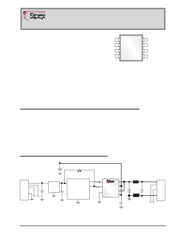
TYPICAL APPLICATION CIRCUIT
One Port Self Powered Hub
DATA
GND
D-
D+
VBUS
IN
OUT
GND
10µF
Cout
10K
+ 1µF
Cin
VIN
ON/OFF
OVERCURRENT
GND
SP2525A
EN
FLG
GND
NC
OUT
IN
OUT
IN
33µF
Ferrite Bead
Ferrite Bead
0.01 µF
DATA
VBUS
D+
D-
GND
VCC
5.0V
0.01 µF
SPX1521
Æ
Æ
USB CONTROLLER
+
+
33µF
4.50V TO 5.25V
UPSTREAM VBUS
100mA MAX
33µF, 16V Tantalum, or
100µF, 10V Electrolytic
Bold line indicate high-current traces
1
2
3
4
5
6
7
8
SP2525A
8 Pin NSOIC
OUT
IN
OUT
GND
EN
FLG
NC
IN
2
Date: 5/3/06 Rev I
SP2525A USB High-Side Power Switch © Copyright 2006 Sipex Corporation
Supply Voltage(
V
IN
)
..........................................7.0V
Fault Flag Voltage (
V
FLG
)
..................................7.0V
Fault Flag Current (
I
FLG
)
..................................50mA
Enable Input (
V
EN
)
...............................-0.3V to 15V
Unless otherwise noted, the following specifications apply for V
IN
= +5.0V, T
A
= 25
∞
C.
Operating Temperature Range.............-40∞C to +85∞C
Storage Temperature Range..............-65∞C to +150∞C
These are stress ratings only and functional operation of the device at these ratings or any other above those indicated
in the operation sections of the specifications below is not implied. Exposure to absolute maximum rating conditions
for extended periods of time may affect reliability.
ABSOLUTE MAXIMUM RATINGS
ELECTRICAL CHARACTERISTICS
Power Dissipation Per Package
8-pin NSOIC
(derate 6.14mW/
O
C above +70
O
C)..................500mW
PARAMETER
MIN.
TYP.
MAX.
UNITS
CONDITIONS
Supply Current
0.75
75
5.0
100
µA
V
EN
= Logic "0" OUT = Open
V
EN
= Logic "1" OUT = Open
Enable Input Voltage
2.4
1.7
2.0
0.8
V
V
EN
= Logic "0"
V
EN
= Logic "1"
Enable Input Current
0.01
0.01
1
1
µA
V
EN
= Logic "0"
V
EN
= Logic "1"
Enable Input Capacitance
1
pF
Output Mosfet Resistance
70
100
m
Output Turn-On Delay
100
µs
R
L
=10 each output
Output Turn-On Rise Time
1000
4000
µs
R
L
=10 each output
Output Turn-Off Delay
0.8
20
µs
R
L
=10 each output
Output Turn-Off Fall Time
0.7
20
µs
R
L
=10 each output
Output Leakage Current
10
µA
Current Limit Threshold
0.6
1.0
1.25
A
Over-Temperature Shutdown
Threshold
135
125
O
C
T
J
increasing
T
J
decreasing
Error Flag Output Resistance
10
15
25
40
V
IN
= 5V,I
L
= 10mA
V
IN
= 3.3V,I
L
= 10mA
Error Flag Off Current
0.01
1
µA
V
FLAG
= 5V
UVLO Threshold
2.6
2.4
V
V
IN
increasing
V
IN
decreasing
3
Date: 5/3/06 Rev I
SP2525A USB High-Side Power Switch © Copyright 2006 Sipex Corporation
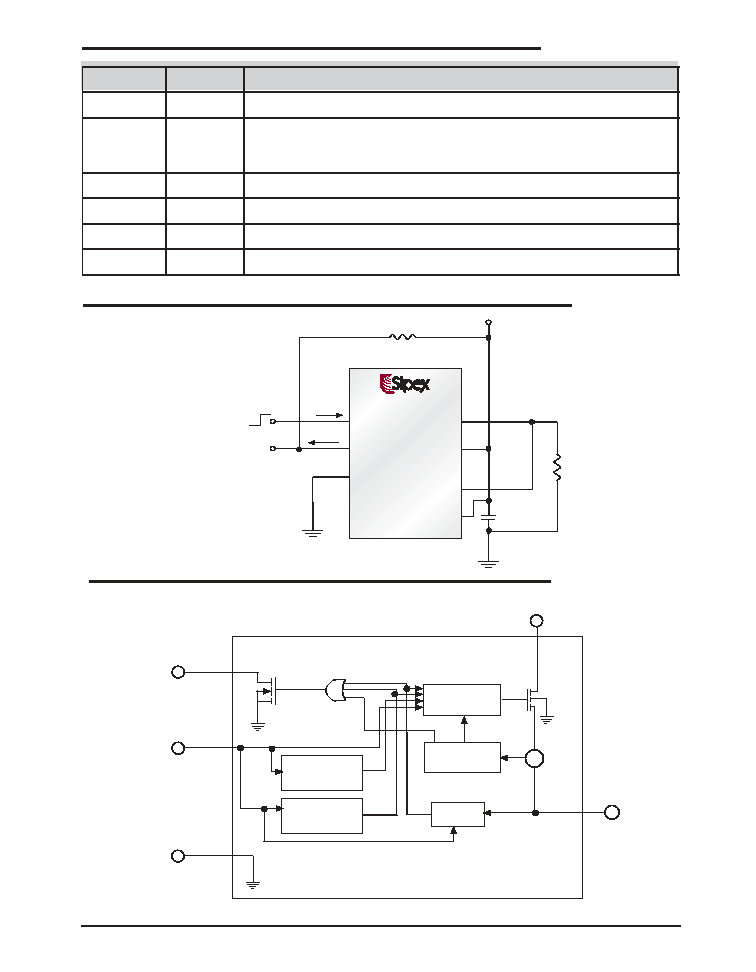
TEST CIRCUIT
PIN DESCRIPTION
OUT
SP2525A
IN
10
V
CC
OUT
IN
EN
FLG
GND
10K
0.1µF
+5V
NC
ON
OFF
Æ
r
e
b
m
u
N
n
i
P
e
m
a
N
n
i
P
n
o
i
t
p
i
r
c
s
e
D
1
N
E
.
2
-
A
5
2
5
2
P
S
r
o
f
w
o
L
e
v
i
t
c
A
d
n
a
1
-
A
5
2
5
2
P
S
r
o
f
h
g
i
H
e
v
i
t
c
A
t
u
p
n
I
e
l
b
a
n
E
2
G
L
F
n
a
c
t
I
.
h
c
t
i
w
s
r
e
w
o
p
r
o
f
t
u
p
t
u
o
g
a
l
f
t
l
u
a
f
d
e
n
i
a
r
d
-
n
e
p
o
d
n
a
w
o
l
-
e
v
i
t
c
a
n
A
n
a
c
o
s
l
a
t
i
,
n
o
i
t
a
r
e
p
o
e
d
o
m
l
a
m
r
o
n
n
I
.
e
v
i
t
c
a
s
i
L
T
C
f
i
t
i
m
il
t
n
e
r
r
u
c
e
t
a
c
i
d
n
i
.
e
g
a
t
l
o
v
r
e
d
n
u
r
o
n
w
o
d
t
u
h
s
l
a
m
r
e
h
t
e
t
a
c
i
d
n
i
3
D
N
G
.
d
n
u
o
r
g
r
e
w
o
p
p
i
h
C
4
C
N
.
d
e
t
c
e
n
n
o
c
y
ll
a
n
r
e
t
n
i
t
o
N
7
,
5
N
I
.
t
u
p
n
i
y
l
p
p
u
s
r
e
w
o
P
8
,
6
T
U
O
.
t
u
p
t
u
o
h
c
t
i
w
s
T
E
F
S
O
M
Current
Limit
CS
OUT
Charge
Pump
UVLO
Thermal
Shutdown
Driver
FLG
EN
IN
Power N-MOSFET
GND
BLOCK DIAGRAM

4
Date: 5/3/06 Rev I
SP2525A USB High-Side Power Switch © Copyright 2006 Sipex Corporation
Error Flag
The Error Flag is an open-drained output of
an N-channel MOSFET, the FLG output is
pulled low to signal the following fault con-
ditions: input undervoltage, output current
limit, and thermal shutdown.
Current Limit
The current limit threshold is preset inter-
nally. It protects the output MOSFET
switches from damage resulting from un-
desirable short circuit conditions or excess
inrush current, which is often encountered
during hot plug-in. The low limit of the
current limit threshold of the SP2525A al-
lows a minimum current of 0.5A through the
MOSFET switches. A current limit condi-
tion will signal the Error Flag.
Thermal Shutdown
When the temperature of the SP2525A
exceeds 135∫C for any reasons, the ther-
mal shutdown function turns off the
MOSFET switch and signals the Error Flag.
A hysteresis of 10∫C prevents the MOSFETs
from turning back on until the chip tempera-
ture drops below 125∫C.
Supply Filtering
A 0.1µF to 1µF bypass capacitor from IN to
GND, located near the device, is strongly
recommended to control supply transients.
Without a bypass capacitor, an output short
may cause ringing on the input (from sup-
ply lead inductance) which can damage
internal control circuitry.
APPLICATION INFORMATION
Transient Requirements
USB supports dynamic attachment (hot plug-
in) of peripherals. A current surge is caused
by the input capacitance of a downstream
device. Ferrite beads are recommended in
series with all power and ground connector
pins. Ferrite beads reduce EMI and limit the
inrush current during hot-attachment by fil-
tering high-frequency signals.
Short Circuit Transient
Bulk capacitance provides the short-term
transient current needed during a hot-attach-
ment event. A 33 µF/16V tantalum or a 100µF/
10V electrolytic capacitor mounted close to
the downstream connector at each port should
provide sufficient transient drop protection.
Printed Circuit Layout
The Power circuitry of USB printed circuit
boards requires a customized layout to maxi-
mize thermal dissipation and to minimize
voltage drop and EMI.
Input and Output
The independent solid state switch connects
the IN pin to the OUT pin when enabled by a
logic signal at EN. The IN pin is the power
supply connection to the internal circuitry and
the drain of the output MOSFET. The OUT
pin is the source for the MOSFET. Typically,
the current in USB application will flow through
the switch from IN to OUT towards the load.
If V
OUT
is greater than V
IN
when a switch is
enabled, the current will flow from OUT to the
IN pin because the MOSFET channels are
bidirectional when switched on. The output
source is allowed to be externally forced to a
higher voltage than its input without causing
unwanted current flow when the output is
disabled.

5
Date: 5/3/06 Rev I
SP2525A USB High-Side Power Switch © Copyright 2006 Sipex Corporation
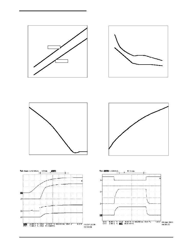
OFF State Supply Current vs. Supply Voltage
0.00
0.02
0.04
0.06
0.08
0.10
3
4
5
6
7
8
Supply Voltage (V)
Supply Current (µA)
ON-State Supply Current vs. Supply Voltage
50
60
70
80
90
100
2
3
4
5
6
7
8
Supply Voltage (V)
Switch-ON Supply Current (µA)
On-state Supply Current vs. Supply Voltage
Output On-Resistance vs. Supply Voltage
Output On-Resistance vs. Temperature
UVLO Threshold Voltage vs. Temperature
TYPICAL PERFORMANCE CHARACTERISTICS
V
IN
= +5.0V, T
AMB
= +25
O
C unless otherwise noted.
UVLO Threshold Voltage vs. Temperature
2.2
2.3
2.4
2.5
2.6
2.7
2.8
-40
-20
0
20
40
60
80
100
120
Temperature (∫C)
UVLO Threshold Voltage (V)
Rising
Falling
ON-State Supply Current vs. Supply Voltage
50
60
70
80
90
100
2
3
4
5
6
7
8
Supply Voltage (V)
Switch-ON Supply Current (µA)
Output On-Resistance vs. Supply Voltage
64
65
66
67
68
69
70
2
3
4
5
6
7
Supply Voltage (V)
Switch-ON Resistance (m)
On-Resistance vs. Temperature
50
60
70
80
90
-60
-40
-20
0
20
40
60
80
100
120
Temperature (∞C)
ON Resistance (m)
Off-state Supply Current vs. Supply Voltage
On-state Supply Current vs. Temperature
6
Date: 5/3/06 Rev I
SP2525A USB High-Side Power Switch © Copyright 2006 Sipex Corporation
Output Rise Time vs. Temperature
Output Fall Time vs. Temperature
0.38
0.40
0.42
0.44
0.46
0.48
0.50
0.52
0.54
-40
-20
0
20
40
60
80
100
120
Temperature (∞C)
Turn-off Fall Time (µS)
Output Rise Time vs. Temperature
1.05
1.10
1.15
1.20
1.25
1.30
1.35
1.40
-40
-20
0
20
40
60
80
100
120
Temperature (∞C)
Turn-ON Resistance (mS)
Output Fall Time vs. Temperature
TYPICAL PERFORMANCE CHARACTERISTICS
V
IN
= +5.0V, T
AMB
= +25
O
C unless otherwise noted.
Control Threshold vs. Supply Voltage
CTL Threshold Voltage vs. Supply Voltage
0.80
1.00
1.20
1.40
1.60
1.80
2.00
2.20
2.40
2.60
2.80
2
3
4
5
6
7
Supply Voltage (V)
Threshold Voltage (V)
CTL Rising
CTL Falling
Current Limit Threshold vs. Temperature
Current Limit Threshold vs. Temperature
0.75
0.80
0.85
0.90
0.95
1.00
1.05
1.10
1.15
-60
-40
-20
0
20
40
60
80
100
120
140
Temperature (∞C)
Output Threshold (A)
V
IN
V
FLG
V
OUT
I
OUT
200mA/div
V
EN
=GND
R
L
=35
C
L
=15uF
Input Voltage
Response
V
EN
V
FLG
V
OUT
I
OUT
100mA/div
R
L
=35
C
L
=15uF
Turn-On, Turn-Off
Characteristics

7
Date: 5/3/06 Rev I
SP2525A USB High-Side Power Switch © Copyright 2006 Sipex Corporation
TYPICAL PERFORMANCE CHARACTERISTICS
V
IN
= +5.0V, T
AMB
= +25
O
C unless otherwise noted.
V
EN
V
FLG
V
OUT
I
OUT
100mA/div
R
L
=35
C
L
=33uF
Turn-On, Turn-Off
Characteristics
V
EN
V
FLG
V
OUT
I
OUT
100mA/div
R
L
=35
C
L
=150uF
Turn-On, Turn-Off
Characteristics
V
EN
V
FLG
V
OUT
I
OUT
1A/div
Short Circuit Response
(Enable to Short Circuit)
V
FLG
V
OUT
I
OUT
5A/div
Short Circuit Transient Response
(Short Applied to Output)
V
FLG
V
OUT
I
OUT
1A/div
Current Limit Response
(Ramped Load)
V
FLG
V
OUT
I
OUT
5A/div
Short Circuit Response
(Short Applied to Output)

8
Date: 5/3/06 Rev I
SP2525A USB High-Side Power Switch © Copyright 2006 Sipex Corporation
PACKAGE: 8 Pin NSOIC
FRONT VIEW
L
¯1
Gauge Plane
L2
c
R
R1
¯2
¯
Seating
Plane
h
h
¯1
D
E
E/2
3
2
1
b
e
E1
E1/2
6
8
Pin1 Designator
to be within this
INDEX AREA
(D/2 x E1/2)
TOP VIEW
(L1)
5
4
7
D/2
A
A2
A1
SIDE VIEW
Seating Plane
MIN
NOM
MAX
MIN
NOM
MAX
A
1.35
-
1.75
0.053
-
0.069
A1
0.10
-
0.25
0.004
-
0.010
A2
1.25
-
1.65
0.049
-
0.065
b
0.31
-
0.51
0.012
-
0.020
c
0.17
-
0.25
0.007
-
0.010
E
E1
e
h
0.25
0.50
0.010
-
0.020
L
0.40
-
1.27
0.016
-
0.050
L1
L2
R
0.07
-
-
0.003
-
-
R1
0.07
-
-
0.003
-
-
¯
0∫
-
8∫
0∫
-
8∫
¯1
5∫
-
15∫
5∫
-
15∫
¯2
0∫
-
-
0∫
-
-
D
0.041 REF
SIPEX Pkg Signoff Date/Rev: JL Aug16-05 / Rev A
4.90 BSC
6.00 BSC
3.90 BSC
1.27 BSC
1.04 REF
0.193 BSC
0.25 BSC
0.010 BSC
0.236 BSC
0.050 BSC
0.154 BSC
8 Pin NSOIC JEDEC MS-012 Variation AA
SYMBOL
Dimensions in Millimeters:
Controlling Dimension
Dimensions in Inches
Conversion Factor:
1 Inch = 25.40 mm

9
Date: 5/3/06 Rev I
SP2525A USB High-Side Power Switch © Copyright 2006 Sipex Corporation
Part Number
Temperature Range
Package Types
SP2525A-1EN ................................................. -40∞C to +85∞C ................................................... 8-pin NSOIC
SP2525A-1EN/TR ........................................... -40∞C to +85∞C .................................................. 8-pin NSOIC
SP2525A-2EN ................................................. -40∞C to +85∞C ................................................... 8-pin NSOIC
SP2525A-2EN/TR ........................................... -40∞C to +85∞C .................................................. 8-pin NSOIC
ORDERING INFORMATION
Solved by Sipex
TM
Sipex Corporation reserves the right to make changes to any products described herein. Sipex does not assume any liability arising out of the
application or use of any product or circuit described herein; neither does it convey any license under its patent rights nor the rights of others.
Sipex Corporation
Headquarters and Sales Office
233 South Hillview Drive
Milpitas, CA 95035
TEL: (408) 934-7500
FAX: (408) 935-7600
Available in lead free packaging. To order add "-L" suffix to part number.
Example: SP2525A-1EN/TR = standard; SP2525A-1EN-L/TR = lead free
/TR = Tape and Reel
Pack quantity is 2,500 for 8 pin NSOIC.