 | –≠–ª–µ–∫—Ç—Ä–æ–Ω–Ω—ã–π –∫–æ–º–ø–æ–Ω–µ–Ω—Ç: SP2526A-2 | –°–∫–∞—á–∞—Ç—å:  PDF PDF  ZIP ZIP |
1
Date: 1/4/06
SP2526A Dual USB High-Side Power Switch © Copyright 2006 Sipex Corporation
SP2526A
Dual USB High-Side Power Switch
Æ
APPLICATIONS
USB Power Management
Hot Plug-In Power Supplies
Battery Charger Circuit
Now Available in Lead Free Packaging
Active-High Version: SP2526A-1
Active-Low Version: SP2526A-2
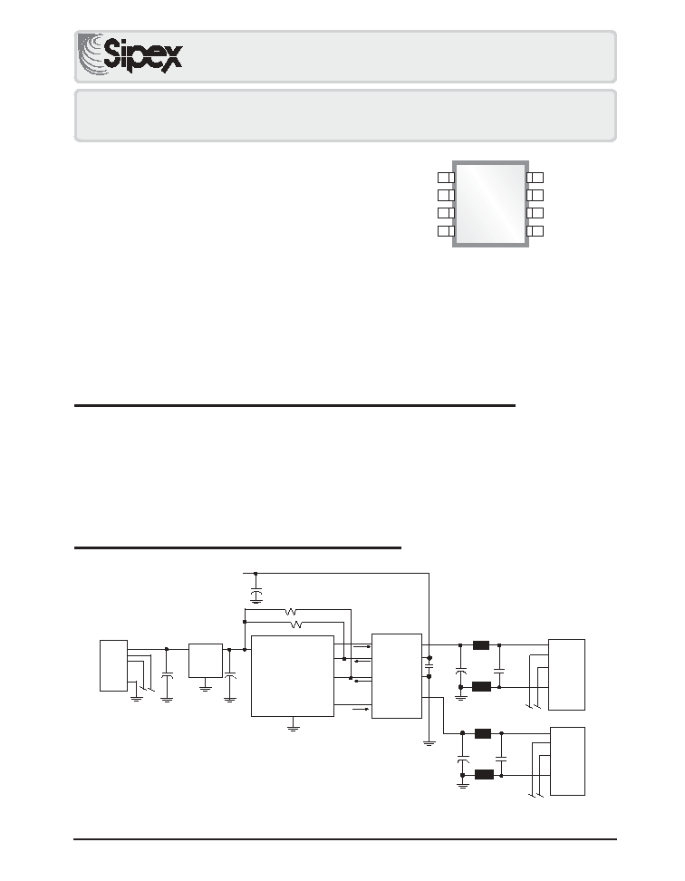
TYPICAL APPLICATION CIRCUIT
FEATURES
+3.0V to +5.5V Input Voltage Range
Two Independent Power Switches
Two Error Flag Outputs, Open Drain
2.6V Undervoltage Lockout
1.25A Short Circuit Current Limit
150m Maximum On-Resistance
110µA On-State Supply Current
1µA Shutdown Current
Output Can Be Forced Higher Than
Input (Off-State)
Thermal Shutdown
1ms Soft-Start Power Up, Fast Turn Off
The SP2526A
device is a dual +3.0V to +5.5V USB Supervisory Power Control Switch ideal
for self-powered and bus-powered Universal Serial Bus (USB) applications. Each switch has
low on-resistance (110m typical) and can supply 500mA minimum. The fault currents are
limited to 1.0A typical and the flag output pin for each switch is available to indicate fault
conditions to the USB controller. The thermal shutdown feature will prevent damage to the
device when subjected to excessive current loads. The undervoltage lockout feature will
ensure that the device will remain off unless there is a valid input voltage present.
DESCRIPTION
1
2
3
4
5
6
7
8
SP2526A
8 Pin NSIOC
OUTA
IN
OUTB
GND
ENA
FLGA
FLGB
ENB
Two Port Self Powered Hub
DATA
GND
D-
D+
VBUS
IN
OUT
GND
10µF
Cout
10K
10K
+ 1µF
Cin
VIN
ON/OFF
OVERCURRENT
OVERCURRENT
ON
GND
SPX1521
ENA
FLGA
FLGB
ENB
OUTA
IN
GND
OUTB
0.1µF
33µF
Ferrite Bead
Ferrite Bead
Ferrite Bead
Ferrite Bead
0.01 µF
0.01 µF
33µF
DATA
DATA
VBUS
D+
D-
GND
VBUS
D+
D-
GND
VCC
5.0V
*
*
*
+
+
+
+
+33µF
USB CONTROLLER
SP2526A
4.50V TO 5.25V
UPSTREAM VBUS
100mA MAX
33µF, 16V Tantalum, or
100µF, 10V Electrolytic
Bold line indicate high-current traces

2
Date: 1/4/06
SP2526A Dual USB High-Side Power Switch © Copyright 2006 Sipex Corporation
Supply Voltage(V
IN
)..........................................7.0V
Fault Flag Voltage (V
FLG
)..................................7.0V
Fault Flag Current (I
FLG
)..................................50mA
Enable Control Input (V
EN
).....................-0.3V -15V
Unless otherwise noted, the following specifications apply for V
IN
= +5.0V, T
A
= 25
∞
C.
Operating Temperature Range.............-40∞C to +85∞C
Maximum Junction Temperature ........................125∞C
Storage Temperature Range..............-65∞C to +150∞C
Soldering Temperature (10 sec.).........................260∞C
Power Dissipation Per Package
8-pin NSOIC (derate 6.14mW/
O
C above +70
O
C)..........500mW
These are stress ratings only and functional operation of the device at these ratings or any other above those indicated
in the operation sections of the specifications below is not implied. Exposure to absolute maximum rating conditions
for extended periods of time may affect reliability.
ABSOLUTE MAXIMUM RATINGS
ELECTRICAL CHARACTERISTICS
R
E
T
E
M
A
R
A
P
.
N
I
M
.
P
Y
T
.
X
A
M
S
T
I
N
U
S
N
O
I
T
I
D
N
O
C
t
n
e
r
r
u
C
y
l
p
p
u
S
5
7
.
0
0
1
1
0
.
5
0
6
1
µA
V
N
E
n
e
p
O
=
T
U
O
"
0
"
c
i
g
o
L
=
V
N
E
n
e
p
O
=
T
U
O
"
1
"
c
i
g
o
L
=
e
g
a
t
l
o
V
t
u
p
n
I
e
l
b
a
n
E
8
.
0
7
.
1
0
.
2
4
.
2
V
V
N
E
"
0
"
c
i
g
o
L
=
V
N
E
"
1
"
c
i
g
o
L
=
t
n
e
r
r
u
C
t
u
p
n
I
e
l
b
a
n
E
1
0
.
0
1
0
.
0
1
1
µA
V
N
E
"
0
"
c
i
g
o
L
=
V
N
E
"
1
"
c
i
g
o
L
=
e
c
n
a
t
i
c
a
p
a
C
t
u
p
n
I
e
l
b
a
n
E
1
F
p
e
c
n
a
t
s
i
s
e
R
t
e
f
s
o
M
t
u
p
t
u
O
0
1
1
0
5
1
m
y
a
l
e
D
n
O
-
n
r
u
T
t
u
p
t
u
O
0
0
1
µs
R
L
0
1
=
t
u
p
t
u
o
h
c
a
e
e
m
i
T
e
s
i
R
n
O
-
n
r
u
T
t
u
p
t
u
O
0
0
0
1
0
0
0
4
µs
R
L
0
1
=
t
u
p
t
u
o
h
c
a
e
y
a
l
e
D
f
f
O
-
n
r
u
T
t
u
p
t
u
O
8
.
0
0
2
µs
R
L
0
1
=
t
u
p
t
u
o
h
c
a
e
e
m
i
T
ll
a
F
f
f
O
-
n
r
u
T
t
u
p
t
u
O
7
.
0
0
2
µs
R
L
0
1
=
t
u
p
t
u
o
h
c
a
e
t
n
e
r
r
u
C
e
g
a
k
a
e
L
t
u
p
t
u
O
0
1
µA
d
l
o
h
s
e
r
h
T
t
i
m
i
L
t
n
e
r
r
u
C
6
.
0
0
.
1
5
2
.
1
A
n
w
o
d
t
u
h
S
e
r
u
t
a
r
e
p
m
e
T
-
r
e
v
O
d
l
o
h
s
e
r
h
T
5
3
1
5
2
1
O
C
T
J
g
n
i
s
a
e
r
c
n
i
T
J
g
n
i
s
a
e
r
c
e
d
e
c
n
a
t
s
i
s
e
R
t
u
p
t
u
O
g
a
l
F
r
o
r
r
E
0
1
5
1
5
2
0
4
V
N
I
I
,
V
5
=
L
A
m
0
1
=
V
N
I
I
,
V
3
.
3
=
L
A
m
0
1
=
t
n
e
r
r
u
C
f
f
O
g
a
l
F
r
o
r
r
E
1
0
.
0
1
µA
V
G
A
L
F
V
5
=
d
l
o
h
s
e
r
h
T
O
L
V
U
6
.
2
4
.
2
V
V
N
I
g
n
i
s
a
e
r
c
n
i
V
N
I
g
n
i
s
a
e
r
c
e
d
3
Date: 1/4/06
SP2526A Dual USB High-Side Power Switch © Copyright 2006 Sipex Corporation
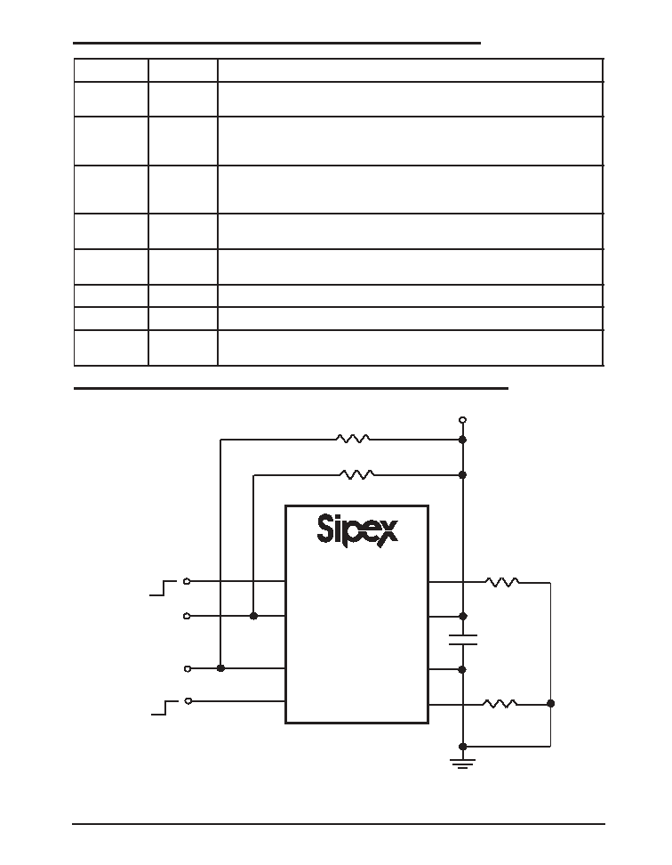
TEST CIRCUIT
PIN DESCRIPTION
GND
SP2526A
IN
10
V
CC
10
OUTA
OUTB
ENA
FLGA
FLGB
ENB
10K R1
10K R2
R4
R4
0.1µF
C1
+5V
ON
ON
OFF
OFF
r
e
b
m
u
N
n
i
P
e
m
a
N
n
i
P
n
o
i
t
p
i
r
c
s
e
D
1
A
N
E
e
h
t
r
o
f
h
g
i
h
e
v
i
t
c
a
s
i
n
i
p
t
u
p
n
i
s
i
h
T
.
A
h
c
t
i
w
S
T
E
F
S
O
M
r
o
f
t
u
p
n
I
e
l
b
a
n
E
2
-
A
6
2
5
2
P
S
e
h
t
r
o
f
w
o
l
e
v
i
t
c
a
d
n
a
1
-
A
6
2
5
2
P
S
2
A
G
L
F
e
t
a
c
i
d
n
i
n
a
c
t
I
.
A
l
e
n
n
a
h
c
t
o
f
t
u
p
t
u
o
g
a
l
f
t
l
u
a
f
d
e
n
i
a
r
d
-
n
e
p
o
d
n
a
w
o
l
-
e
v
i
t
c
a
n
A
B
N
E
d
n
a
/
r
o
A
N
E
(
n
o
i
t
a
r
e
p
o
e
d
o
m
l
a
m
r
o
n
n
I
.
e
v
i
t
c
a
s
i
A
N
E
n
e
h
w
t
i
m
il
t
n
e
r
r
u
c
.
e
g
a
t
l
o
v
r
e
d
n
u
r
o
n
w
o
d
u
h
s
l
a
m
r
e
h
t
e
t
a
c
i
d
n
i
n
a
c
o
s
l
a
t
i
,
)
e
v
i
t
c
a
s
i
3
B
G
L
F
e
t
a
c
i
d
n
i
n
a
c
t
I
.
B
l
e
n
n
a
h
c
t
o
f
t
u
p
t
u
o
g
a
l
f
t
l
u
a
f
d
e
n
i
a
r
d
-
n
e
p
o
d
n
a
w
o
l
-
e
v
i
t
c
a
n
A
B
N
E
d
n
a
/
r
o
A
N
E
(
n
o
i
t
a
r
e
p
o
e
d
o
m
l
a
m
r
o
n
n
I
.
e
v
i
t
c
a
s
i
B
N
E
n
e
h
w
t
i
m
il
t
n
e
r
r
u
c
.
e
g
a
t
l
o
v
r
e
d
n
u
r
o
n
w
o
d
u
h
s
l
a
m
r
e
h
t
e
t
a
c
i
d
n
i
n
a
c
o
s
l
a
t
i
,
)
e
v
i
t
c
a
s
i
4
B
N
E
e
h
t
r
o
f
h
g
i
h
e
v
i
t
c
a
s
i
n
i
p
t
u
p
n
i
s
i
h
T
.
B
h
c
t
i
w
S
T
E
F
S
O
M
r
o
f
t
u
p
n
I
e
l
b
a
n
E
2
-
A
6
2
5
2
P
S
e
h
t
r
o
f
w
o
l
e
v
i
t
c
a
d
n
a
1
-
A
6
2
5
2
P
S
5
B
T
U
O
T
E
F
S
O
M
e
h
t
f
o
n
i
p
t
u
p
t
u
o
e
h
t
s
i
s
i
h
T
.
B
l
e
n
n
a
h
C
h
c
t
i
w
S
T
E
F
S
O
M
r
o
f
t
u
p
t
u
O
.
d
a
o
l
e
h
t
f
o
e
d
i
s
d
e
h
c
t
i
w
s
e
h
t
o
t
d
e
t
c
e
n
n
o
c
y
ll
a
c
i
p
y
t
,
B
l
e
n
n
a
h
c
f
o
e
c
r
u
o
s
6
D
N
G
.
d
n
u
o
r
G
7
N
I
t
u
p
n
i
y
l
p
p
u
s
r
e
w
o
P
8
A
T
U
O
T
E
F
S
O
M
e
h
t
f
o
n
i
p
t
u
p
t
u
o
e
h
t
s
i
s
i
h
T
.
A
l
e
n
n
a
h
C
h
c
t
i
w
S
T
E
F
S
O
M
r
o
f
t
u
p
t
u
O
.
d
a
o
l
e
h
t
f
o
e
d
i
s
d
e
h
c
t
i
w
s
e
h
t
o
t
d
e
t
c
e
n
n
o
c
y
ll
a
c
i
p
y
t
,
A
l
e
n
n
a
h
c
f
o
e
c
r
u
o
s

4
Date: 1/4/06
SP2526A Dual USB High-Side Power Switch © Copyright 2006 Sipex Corporation
Error Flag
An open-drained output of an N-channel
MOSFET, the FLG output is pulled low to
signal the following fault conditions: input
undervoltage, output current limit, and thermal
shutdown.
Current Limit
The current limit threshold is preset internally.
It protects the output MOSFET switches from
damage resulting from undesirable short circuit
conditions or excess inrush current, which is
often encountered during hot plug-in. The low
limit of the current limit threshold of the
SP2526A allows a minimum current of 0.6A
through the MOSFET switches. A current limit
condition will signal the error flag.
Thermal Shutdown
When the chip temperature exceeds 135∫C for
any reason other than overcurrent fault of either
one of the two MOSFETs, the thermal shut-
down function turns off both MOSFET switches
and signals the error flag. A hysteresis of 10∫C
prevents the MOSFETs from turning back on
until the chip temperature drops below 125∫C.
However, if thermal shutdown is triggered by
chip temperature rise resulting from overcurrent
fault condition of either one of the MOSFET
switches, the thermal shutdown function will
only turn off the switch that is in overcurrent
condition and the other switch can still remain
its normal operation. In other words, the ther-
mal shutdown function of the two switches is
independent of each other in the case of
overcurrent fault.
Supply Filtering
A 0.1
µF to 1µF bypass capacitor from IN to
GND, located near the device, is strongly recom-
mended to control supply transients. Without a
bypass capacitor, an output short may cause
sufficient ringing on the input (from supply lead
inductance) to damage internal control circuitry.
Transient Requirements
USB supports dynamic attachment (hot plug-in)
of peripherals. A current surge is caused by the
input capacitance of downstream device. Ferrite
beads are recommended in series with all power
and ground connector pins. Ferrite beads reduce
EMI and limit the inrush current during hot-
attachment by filtering high-frequency signals.
Short Circuit Transient
Bulk capacitance provides the short-term tran-
sient current needed during a hot-attachment event.
A 33
µF,16V tantalum or a 100µF,10V electro-
lytic capacitor mounted close to downstream con-
nector each port should provide transient drop
protection
Printed Circuit Layout
The Power circuitry of USB printed circuit boards
requires a customized layout to maximize ther-
mal dissipation and to minimize voltage drop and
EMI.
APPLICATION INFORMATION
5
Date: 1/4/06
SP2526A Dual USB High-Side Power Switch © Copyright 2006 Sipex Corporation
BLOCK DIAGRAM
Current
Limit
CS
OUTA
Charge
Pump
UVLO
Thermal
Shutdown
Current
Limit
Driver
Driver
Charge
Pump
CS
FLGA
ENA
ENB
FLGB
OUTB
IN
Power N-MOSFET
Power N-MOSFET
6
Date: 1/4/06
SP2526A Dual USB High-Side Power Switch © Copyright 2006 Sipex Corporation
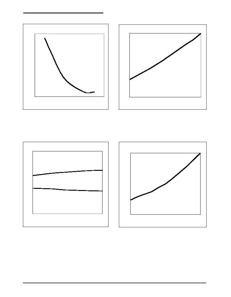
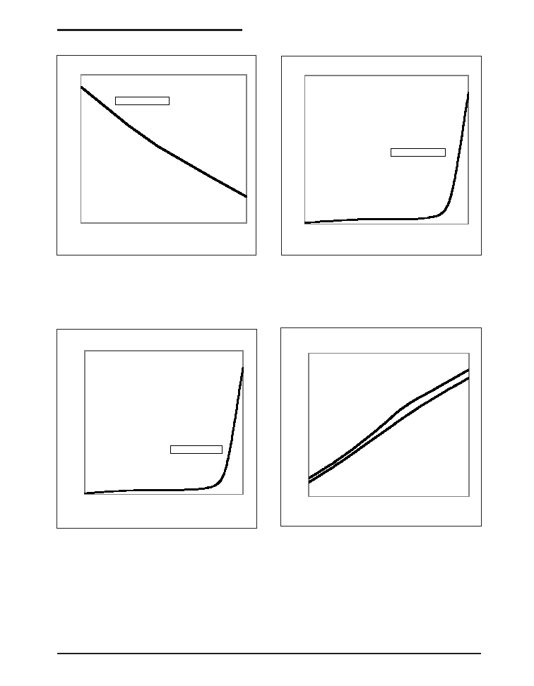
Figure 4. On-state Supply Current vs. Supply Voltage
Figure 1. Output On-Resistance vs. Supply Voltage
Figure 2. Output On-Resistance vs. Temperature
Figure 3. UVLO Threshold Voltage vs. Temperature
TYPICAL PERFORMANCE CHARACTERISTICS
V
IN
= +5.0V, single MOSFET switch section, and T
AMB
= +25
O
C unless otherwise noted.
On-Resistance (millohms)
Output-On-Resistance (millohms)
UVLO Threshold Voltage (V)
Enable Threshold Voltage (V)
R
L
= 47
T
A
= 25∫C
104
106
108
110
112
114
116
118
2.5
3
3.5
4
4.5
5
5.5
6
Supply Voltage (V)
60
70
80
90
100
110
120
130
140
-40
-20
0
20
40
60
80
100
Temperature (∞C)
R
L
= 47
T
A
= 25∫C
2
2.2
2.4
2.6
2.8
3
-40
-20
0
20
40
60
80
100
Temperature (∞C)
Rising
Falling
Both Switches On
60
80
100
120
140
160
3
4
5
6
7
8
Supply Voltage (V)
7
Date: 1/4/06
SP2526A Dual USB High-Side Power Switch © Copyright 2006 Sipex Corporation
Figure 7. Off-state Supply Current vs. Supply Voltage
Figure 5. On-state Supply Current vs. Temperature
Figure 6. Off-state Supply Current vs. Temperature
TYPICAL PERFORMANCE CHARACTERISTICS
V
IN
= +5.0V, single MOSFET switch section, and T
AMB
= +25
O
C unless otherwise noted.
Supply Current (
µ
µ
µ
µ
µ
A)
Offstate Supply Current (
µ
µ
µ
µ
µ
A)
Supply Current (
µ
µ
µ
µ
µ
A)
Offstate Supply Current (
µ
µ
µ
µ
µ
A)
Figure 8. Control Threshold vs. Supply Voltage
80
90
100
110
120
130
-40
-20
0
20
40
60
80
100
Temperature (∞C)
Switches Enabled
1.0
1.1
1.2
1.3
1.4
1.5
1.6
1.7
3
3.5
4
4.5
5
5.5
Supply Voltage (V)
Enable Voltage Rising
Enable Voltage Falling
0.00
0.02
0.04
0.06
0.08
0.10
-40
-20
0
20
40
60
80
100
Temperature (∞C)
Switches Disabled
0.00
0.02
0.04
0.06
0.08
0.10
-40
-20
0
20
40
60
80
100
Temperature (∞C)
Both Switches Off
8
Date: 1/4/06
SP2526A Dual USB High-Side Power Switch © Copyright 2006 Sipex Corporation
TYPICAL PERFORMANCE CHARACTERISTICS
V
IN
= +5.0V, single MOSFET switch section, and T
AMB
= +25
O
C unless otherwise noted.
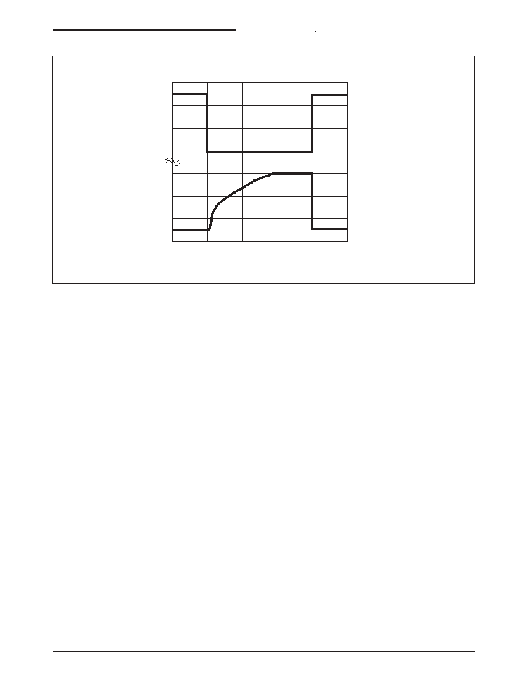
Figure 9. Turn-on/Turn-off Characteristics
-1
1
3
5
0
2
4
6
0
0.5
1.5
2.0
2.5
1.0
Output (V)
Control (V)
RL = 47
Time (mS)
9
Date: 1/4/06
SP2526A Dual USB High-Side Power Switch © Copyright 2006 Sipex Corporation
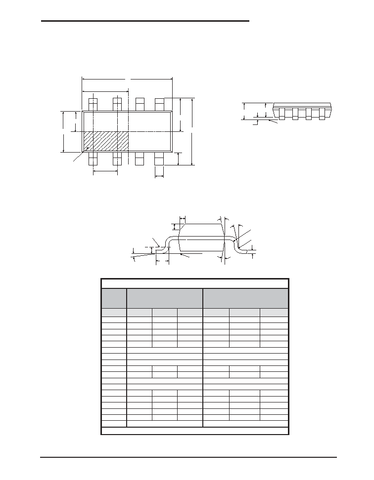
PACKAGE: 8 Pin NSOIC
FRONT VIEW
L
¯1
Gauge Plane
L2
c
R
R1
¯2
¯
Seating
Plane
h
h
¯1
D
E
E/2
3
2
1
b
e
E1
E1/2
6
8
Pin1 Designator
to be within this
INDEX AREA
(D/2 x E1/2)
TOP VIEW
(L1)
5
4
7
D/2
A
A2
A1
SIDE VIEW
Seating Plane
MIN
NOM
MAX
MIN
NOM
MAX
A
1.35
-
1.75
0.053
-
0.069
A1
0.10
-
0.25
0.004
-
0.010
A2
1.25
-
1.65
0.049
-
0.065
b
0.31
-
0.51
0.012
-
0.020
c
0.17
-
0.25
0.007
-
0.010
E
E1
e
h
0.25
0.50
0.010
-
0.020
L
0.40
-
1.27
0.016
-
0.050
L1
L2
R
0.07
-
-
0.003
-
-
R1
0.07
-
-
0.003
-
-
¯
0∫
-
8∫
0∫
-
8∫
¯1
5∫
-
15∫
5∫
-
15∫
¯2
0∫
-
-
0∫
-
-
D
0.041 REF
SIPEX Pkg Signoff Date/Rev: JL Aug16-05 / Rev A
4.90 BSC
6.00 BSC
3.90 BSC
1.27 BSC
1.04 REF
0.193 BSC
0.25 BSC
0.010 BSC
0.236 BSC
0.050 BSC
0.154 BSC
8 Pin NSOIC JEDEC MS-012 Variation AA
SYMBOL
Dimensions in Millimeters:
Controlling Dimension
Dimensions in Inches
Conversion Factor:
1 Inch = 25.40 mm
10
Date: 1/4/06
SP2526A Dual USB High-Side Power Switch © Copyright 2006 Sipex Corporation
Part Number
Temperature Range
Package Types
SP2526A-1EN ................................................. -40∞C to +85∞C ................................................... 8-pin NSOIC
SP2526A-1EN/TR ........................................... -40∞C to +85∞C .................................................. 8-pin NSOIC
SP2526A-2EN ................................................. -40∞C to +85∞C ................................................... 8-pin NSOIC
SP2526A-2EN/TR ........................................... -40∞C to +85∞C .................................................. 8-pin NSOIC
ORDERING INFORMATION
Corporation
ANALOG EXCELLENCE
Sipex Corporation reserves the right to make changes to any products described herein. Sipex does not assume any liability arising out of the
application or use of any product or circuit described herein; neither does it convey any license under its patent rights nor the rights of others.
Sipex Corporation
Headquarters and
Sales Office
233 South Hillview Drive
Milpitas, CA 95035
TEL: (408) 934-7500
FAX: (408) 935-7600
Available in lead free packaging. To order add "-L" suffix to part number.
Example: SP2526A-1EN/TR = standard; SP2526A-1EN-L/TR = lead free.
/TR = Tape and Reel
Pack quantity is 2,500 for NSOIC.