 | –≠–ª–µ–∫—Ç—Ä–æ–Ω–Ω—ã–π –∫–æ–º–ø–æ–Ω–µ–Ω—Ç: SP2526EB | –°–∫–∞—á–∞—Ç—å:  PDF PDF  ZIP ZIP |
SP2526EB/02
SP2526 Evaluation Board Manual
© Copyright 2000 Sipex Corporation
1
The SP2526 Evaluation Board is designed to help the user evaluate the performance of
the SP2526 for use as a dual +3.0V to +5.5V USB Supervisory Control Switch. Each channel
of the SP2526 can be evaluated for its low on-resistance and capacity to supply 500mA
output current. The SP2526 Evaluation Board is designed with independent V
DD
and V
IN
connections to make it easy to measure the very low quiescent current of 100
µ
A maximum,
and low PC board resistance for evaluating the very low on-resistance of 100m
maximum.
The evaluation board is a completely assembled and tested surface mount board which
provides easy probe access points to all SP2526 Inputs and Outputs so that the user can
quickly connect and measure electrical characteristics and waveforms.
DESCRIPTION
SP2526
Evaluation Board Manual
s
Easy Evaluation for the
SP2526 USB Compliant
Power Control Switch
s
SP2526NEB contains 2
Independent USB Power
Switches with +3.0V to
+5.5V Input Range
s
Low PC Board
Resistance for testing
100m
Max On
Resistance of SP2526
s
Evaluation Board
complete with all
capacitors & ferrite
beads to implement a
USB Compliant Power Port
s
Pin-to-Pin Compatible
with Micrel MIC2526

SP2526EB/02
SP2526 Evaluation Board Manual
© Copyright 2000 Sipex Corporation
2
SP2526 EVALUATION BOARD
The next two sections describe the SP2526 Board
Layout and Using the SP2526 Evaluation
Boards. A table of SP2526 Pin Assignments is
also included with details on Input/Output pin
function. A SP2526 Evaluation Board List
of Materials table is provided with some
manufacturers part numbers to use as a
reference. Finally, a schematic and drawings of
the PC Board Layout are included of the
SP2526 Evaluation Board.
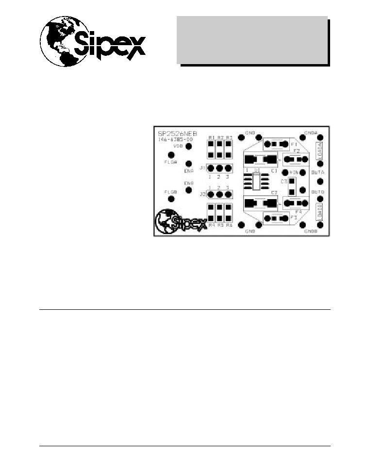
BOARD LAYOUT
The SP2526 Evaluation Board has been
designed to easily and conveniently provide
access to all Inputs and Outputs of the SP2526
device under test. Position the board with the
silkscreen lettering upright (see Figure 1
Component Layout) and you will see the
SP2526 SOIC labeled U1 in the center right of
the board, and around it the Capacitors C1,2,3
and Ferrite Beads F1-4 forming the Dual USB
Supervisory Switch.
The SP2526 Evaluation Board provides solder
pads to connect wires to an external power
supply and load, as well as Test Point Posts
to monitor the Input and Output Voltages at
these connections to the SP2526. The SP2526
PC Board Layout has been designed with low
resistance input and output connections of 2m
each to provide the lowest On-Resistance for
utilizing the USB Switch.
The PC Layout is given in Figures 1-3 for the
user as an aid in designing a low resistance USB
switch on a PC board. The PC board used has 1oz
Copper with V
IN
, Ground, V
OUT
traces of at least
0.1inch width for 5m
/inch or looked at another
way as 0.5m
/square. This means to maintain a
trace resistance of only 2m
, you need to have
only 4 squares of trace from one end to another.
Resistance is further reduced by some additional
wide V
IN
, Ground and V
OUT
connections on the
bottom side of the PC board which are connected
to the top side with large through-hole
connections. For best results with on-resistance
in the ferrites used for EMI suppression in the
Output and Ground connections, through-hole
ferrite beads were used for F1-4, yielding 2m
per input or output connection versus using
surface-mount size 0805 ferrite beads which
yielded 5m
per input or output connection.
USING THE EVALUATION BOARD
The SP2526 Evaluation Board can be connected
to a power supply using a pair of wires soldered
to the solder pads marked provided "VIN" and
"GND". It is good practice to not switch power
on until power connections are made to the
evaluation board.
Powering Up & Using the SP2526 Circuit
V
IN
-- U1-7 -- Solder wire to VIN solder
pad on component side of board and connect to
external Power Supply positive. V
IN
= +3.0V
to +5.5V. Connect Voltmeter positive or
Oscilloscope probe to V
IN
test point post to
monitor actual voltage input to PC board.
GND -- U1-6 -- Solder wire to GND solder
pad on component side of board and connect to
external Power Supply negative. Connect
Voltmeter negative or Oscilloscope probe
ground to GND
test point post to monitor
actual voltage input to PC board.
OUTA -- U1-8 -- Solder wire to OUTA solder
pad on component side of board and connect
to external load. Connect Voltmeter positive
or Oscilloscope probe to OUTA
test point post
to monitor actual voltage output at the PC board.
GNDA -- Solder wire to GNDA solder pad
on component side of board and connect to
external LoadA return. Connect Voltmeter
negative or Oscilloscope probe ground to
GND
test point post to monitor actual voltage
input to PC board.
OUTB -- U1-5 -- Solder wire to OUTB solder
pad on component side of board and connect
to external load. Connect Voltmeter positive
or Oscilloscope probe to OUTB
test point post
to monitor actual voltage output at the PC board.
GNDB -- Solder wire to GNDB solder pad on
component side of board and connect to external
LoadB return. Connect Voltmeter negative or
Oscilloscope probe ground to GND
test point post
to monitor actual voltage input to PC board.

SP2526EB/02
SP2526 Evaluation Board Manual
© Copyright 2000 Sipex Corporation
3
V
DD
-- Connect to a second Power Supply 5V
(or 3.3V) connection ≠ V
DD
provides the pull-up
voltage for Enables ENA & ENB and Flags
FLGA & FLGB. This separate supply connection
allows the user to separately measure V
IN
supply
current.
GND -- Second Power Supply GND Connection ≠
connect to supply return for V
DD
.
ENA -- U1-1 --Enable A Input must be
connected High or Low ≠ open produces
unstable behavior, so be sure to connect V
DD
to
an external 3.3V or 5V source. See Table 1
Enable Jumpers for information on Enable
Jumper J1 position. The user can actively
control Switch A with an external Logic signal.
FLGA -- U1-2 -- Flag A output is open drain
and has a pull-up to V
DD
(which should be
connected to an external source). Connect
FLGA to voltmeter or oscilloscope to monitor
Switch A for flags when Low if Under-voltage,
Over-current or Over-temperature occurs.
.
ENB -- U1-4 -- Enable B Input must be
connected High or Low ≠ open produces
unstable behavior, so be sure to connect V
DD
to an external 3.3V or 5V source. See Table 1
Enable Jumpers for information on Enable
Jumper J2 position. The user can actively
control Switch B with an external Logic signal.
FLGB -- U1-3 -- Flag B output is open drain
and has a pull-up to V
DD
(which should be
connected to an external source). Connect
FLGB to voltmeter or oscilloscope to monitor
Switch B for flags when Low if Under-voltage,
Over-current or Over-temperature occurs.
Using the Enable Jumbers J1 & J2
The jumpers J1& J2 have 2 positions, as
described below. Connecting a logic level to
the ENA or ENB test point post will override
the pull-up or pull-down to actively control
the switch.
Part
Enable A
Enable B
Number
Enable
J1 Position
J2 Position
SP2526-1
Active
1-2
1-2
High
Pull-up
Pull-up
SP2526-2
Active
2-3
2-3
Low
Pull-down
Pull-down
Table 1. Enable Jumpers J1 & J2
SP2526EB/02
SP2526 Evaluation Board Manual
© Copyright 2000 Sipex Corporation
4
SP2526EB Pin Assignments
Pin #
Pin Name
Pin Function Input/Output Pin Name
SP2526-1
1
ENA
Enable A Input Active High
ENA
2
FLGA Fault Flag A Output Active Low
FLGA
3
FLGB Fault Flag B Output Active Low
FLGB
4
ENB
Enable B Input Active High
ENB
5
OUTB
Switch B Output
OUTB
6
GND
Ground
GND
7
IN
Supply Input
V
IN
8
OUTA
Switch A Output
OUTA
SP2525-2
1
ENA
Enable A Input Active Low
ENA
2
FLGA Fault Flag A Output Active Low
FLGA
3
FLGB Fault Flag B Output Active Low
FLGB
4
ENB
Enable B Input Active Low
ENB
5
OUTB
Switch B Output
OUTB
6
GND
Ground
GND
7
IN
Supply Input
V
IN
8
OUTA
Switch A Output
OUTA
Table 2. SP2526EB PIN ASSIGNMENTS
SP2526EB/02
SP2526 Evaluation Board Manual
© Copyright 2000 Sipex Corporation
5
SP2526 Evaluation Board List of Materials
Ref.
Manuf.
Digi-Key
Layout
Vendor
Des. Qty.
Manuf.
Part Number
Part Number
Size
Component
Phone Number
PCB
1
Sipex
146-6385-00
-
1.2"x1.9"
SP2526 Eval PCB
978-667-7800
U1
1
Sipex
SP2526XCN
-
SO-8
Dual USB Switch
C1,2
2
Kemet
T495D157K010AS
-
"D" SM
6.3V 150uF Low ESR 864-963-6300
C3
1 Panasonic
ECJ-VB1E104K
PCC1883CT-ND
1206 SM
X7R 0.1uF 25V
Digi-Key
F1-4
4 Panasonic
EXC-ELDR25C
P9819BK-ND
7.5X2.2mm
EMI Bead
800-344-4539
F1-4
4 Panasonic
EXC-ELDR35C
P9817BK-ND
9X2.2mm
EMI Bead
Digi-Key
F1-4
4 Panasonic
EXC-L351350
P9823-ND
5X3.5mm
EMI Bead
Digi-Key
F1-4
4 Panasonic
EXC-ML20A390U
P10191CT-ND
0805 SM
SM EMI Bead
Digi-Key
R1-6
6 Panasonic
ERJ-8GEYJ104
P100KECT-ND
1206 SM
100K ohm 1/8W 5%
Digi-Key
TP
12
Mill-Max
3137-3002-10-0080
ED5009-ND
.042 Dia
Test Point Female Pin
Digi-Key
J1,2 2
Sullins
PZC36SAAN
S1011-36-ND
.32x.12
36-Pin (3x12) Header
Digi-Key
2
Sullins
STC02SYAN
S9000-ND
.2x.1
Shunt
Digi-Key
Table 3. SP2526EB LIST OF MATERIALS
SP2526EB/02
SP2526 Evaluation Board Manual
© Copyright 2000 Sipex Corporation
6
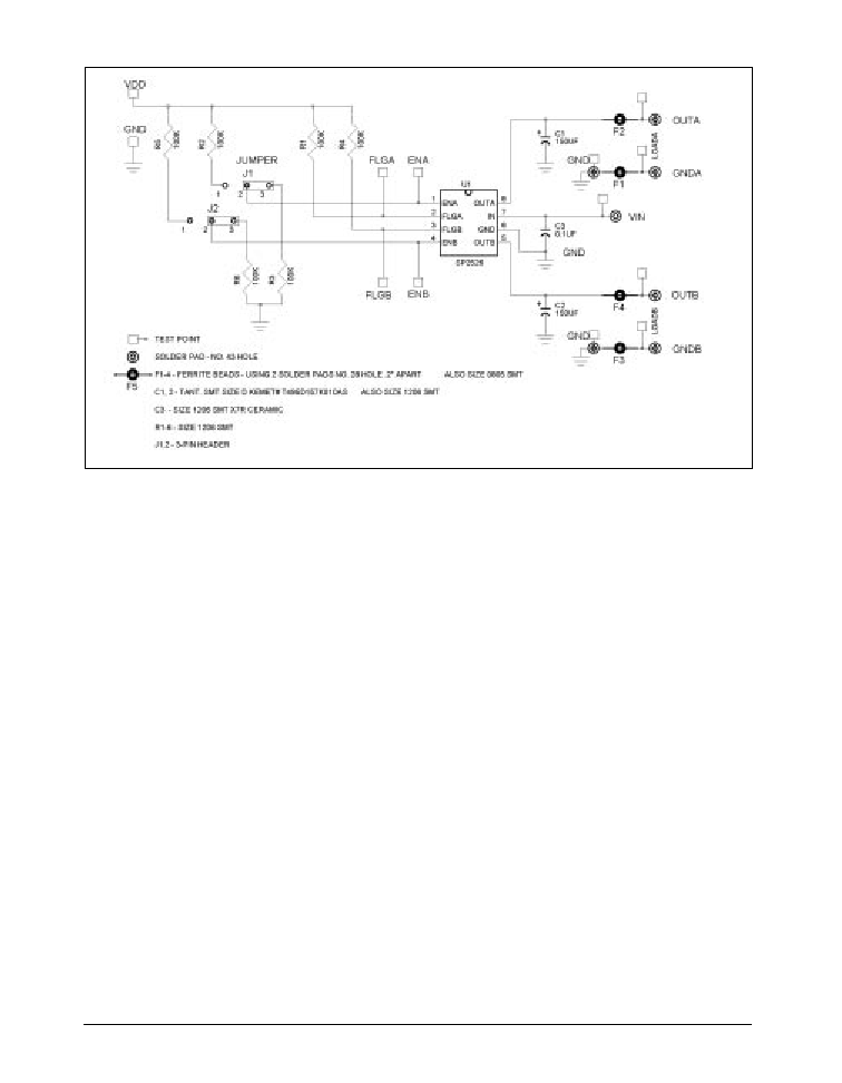
SP2526 Evaluation Board Schematic

SP2526EB/02
SP2526 Evaluation Board Manual
© Copyright 2000 Sipex Corporation
7
Figure 1. SP2526NEB Component Placement
Figure 2. SP2526NEB PC Layout Component Side
Figure 3. SP2526NEB PC Layout Soldier Side

SP2526EB/02
SP2526 Evaluation Board Manual
© Copyright 2000 Sipex Corporation
8
Sipex Corporation reserves the right to make changes to any products described herein. Sipex does not assume any liability arising out of the
application or use of any product or circuit described hereing; neither does it convey any license under its patent rights nor the rights of others.
Corporation
SIGNAL PROCESSING EXCELLENCE
Sipex Corporation
Headquarters and
Sales Office
22 Linnell Circle
Billerica, MA 01821
TEL: (978) 667-8700
FAX: (978) 670-9001
e-mail: sales@sipex.com
Sales Office
233 South Hillview Drive
Milpitas, CA 95035
TEL: (408) 934-7500
FAX: (408) 935-7600
Far East:
JAPAN:
Nippon Sipex Corporation
Yahagi No. 2 Building
3-5-3 Uchikanda, Chiyoda-ku
Tokyo 101, Japan
TEL: 011.81.3.3256.0577
FAX: 011.81.3.3256.0621
European Sales Offices:
GERMANY:
Sipex GmbH
Gautinger Strasse 10
82319 Starnberg
TEL: 49.81.51.89810
FAX: 49.81.51.29598
e-mail: sipex-starnberg@t-online.de
Model
Package
SP2526-1NEB ................................................................................................. SP2526EN-1 Evaluation Board
SP2526-2NEB ................................................................................................. SP2526EN-2 Evaluation Board
ORDERING INFORMATION