 | –≠–ª–µ–∫—Ç—Ä–æ–Ω–Ω—ã–π –∫–æ–º–ø–æ–Ω–µ–Ω—Ç: SP304ET | –°–∫–∞—á–∞—Ç—å:  PDF PDF  ZIP ZIP |
77
Corporation
SIGNAL PROCESSING EXCELLENCE
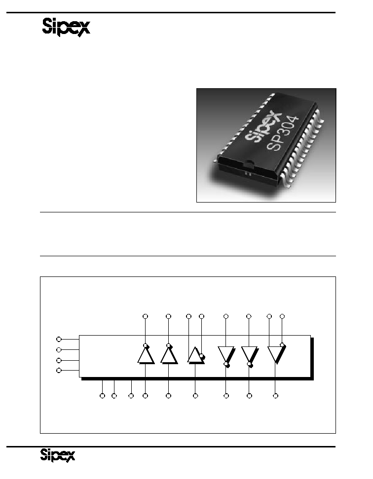
SP304
RS-232/RS-422 Line Drivers/Receivers
s
RS-232 and RS-422 on One Chip
s
Multiple Drivers and Receivers
s
Software-selectable Modes
s
Loopback for Self-Testing
s
Short-circuit Protected
s
Single-width 24-pin DIP and 28≠pin
SOIC Packages
DESCRIPTION...
The SP304 is an enhanced-performance version of the Sipex SP302 RS-232 and RS-422
protocol line drivers and receivers. It is pin-for-pin compatible with the SP302, and in any
configuration, fully meets the requirements of the EIA RS-232D and RS-422 data communication
standards. A loopback test mode is provided.The SP304 is available in 24-pin single width plastic
DIP, and 28-pin SOIC packages for commercial and industrial temperature range operation.
RIB
1
ROB
1
TOB
1
TIB
1
RIA
1
ROA
1
TOA
1
TIA
1
SELECT
A B
TOA
2
RIA
2
TOB
2
TIB
2
RIB
2
ROB
2
V
DD
GND
V
CC
V
EE
SP304
LOOP≠
BACK
Corporation
SIGNAL PROCESSING EXCELLENCE
Corporation
SIGNAL PROCESSING EXCELLENCE
78
SPECIFICATIONS
(T
MIN
T
A
T
MAX
and nominal supply voltages unless otherwise noted)
PARAMETER
MIN.
TYP.
MAX.
UNITS
CONDITIONS
RS-232 DRIVER
TTL Input Level
V
IL
0
0.8
V
V
IH
2.0
V
High Level Output
+5.0
V
R
L
= 3k
, V
IN
= 0.8V
Low Level Output
-5.0
V
R
L
= 3k
, V
IN
= 2.0V
Short Circuit Current
±
30
mA
V
OUT
= 0V
Loopback Output Voltage
-1.5
V
R
L
= 3k
, V
EE
= -12.0V; Note 1
Slew rate
30
V/
µ
s
C
L
= 50pF, R
L
= 3k
; T
A
=
25
∞
C
Transition Time
3
µ
s
V
OUT
from +3V to -3V
or -3V to +3V
Maximum Transmission Rate
200
kbps
RS-232 RECEIVER
Input Voltage Range
-15
+15
V
Note 6
Input High Threshold
+1.75
+2.5
V
Positive-going
Input Low Threshold
+0.75
+1.35
V
Negative-going
Input Impedance
3
7
k
TTL Output Level
V
OL
0.4
V
V
CC
= +4.75V, I
OUT
= +1.6mA
V
OH
2.4
V
V
CC
= +4.75V, I
OUT
= -0.5mA
Maximum Receiving Rate
200
kbps
RS-422 DRIVER
TTL Input Level
V
IL
0
0.8
V
V
IH
2.0
V
High Level Output
2.75
6.0
V
I
OH
= -20mA
Low Level Output
1.0
V
I
OL
= +20mA
Differential Output
±
2
V
R
L
= 100
±
6
V
R
L
=
Short Circuit Current
±
100
mA
Note 2
Output Current
±
500
µ
A
-0.25V
V
O
6V; power off
Transition Time
400
ns
R
L
= 100
, C
L
= 15pF; Note 3
Maximum Transmission Rate
1,000
kbps
RS-422 RECEIVER
Common Mode Range
±
7
V
Note 4
Differential Input
±
15
V
Note 4
Differential Input Threshold
-0.2
+0.2
V
T
A
= 25
∞
C
Input Voltage Hysteresis
30
mV
V
CM
= 0V; T
A
= 25
∞
C
Input Resistance
3
k
-7V
V
CM
+7V
TTL Output Level
V
OL
0.4
V
V
CC
= +4.75V, I
OUT
= +1.6mA
V
OH
2.4
V
V
CC
= +4.75V, I
OUT
= -0.5mA
Maximum Receiving Rate
1,000
kbps
Short Circuit Output Current
±
120
mA
V
OUT
= 0V
POWER REQUIREMENTS
V
DD
= +12V,
±
10%
7
15
mA
Note 5
V
CC
= +5V,
±
10%
5
7
mA
Note 5
V
EE
= -12V,
±
10%
11
20
mA
Note 5
ENVIRONMENTAL
Operating Temperature
-CS
0
+70
∞
C
-MR
-55
+125
∞
C
Storage Temperature
-65
+150
∞
C
79
Corporation
SIGNAL PROCESSING EXCELLENCE
Notes:
1.
In Loopback mode
2.
Only one output drive pin per package will be shorted at any time
3.
From 10% to 90% of steady-state
4.
This is an absolute maximum rating; normal operating levels are V
IN
< 5V
5.
Outputs unloaded; Inputs tied to GND; T
A
= +25
∞
C; V
IL
= 0V; LB=0
Typical SP304 current drains under full load are:
18mA (+12V), 10mA (-12V) and 7mA (+5V) in RS-232 mode only;
5mA (+12V), 7mA (-12V) and 56mA (+5V) in RS-422 mode only;
12mA (+12V), 14mA (-12V) and 31mA (+5V) in RS-232 and RS-422 modes;
RS232 loads 3k
, 2500pF, 20kHz; RS422 outputs across 100
, 500kHz.
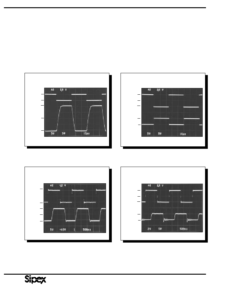
RS-422 Driver
2V
GND
5V
GND
≠5V
T
IN
T
OUT
500kHz
5V
GND
10V
GND
≠10V
T
I N
T
O U T
20kHz
RS-232 Driver
RS-422 Receiver
500kHz
2V
GND
≠2V
5V
GND
R
IN
R
OUT
20kHz
5V
GND
≠5V
5V
GND
R
IN
R
OUT
RS-232 Receiver
TYPICAL PERFORMANCE CURVES
Corporation
SIGNAL PROCESSING EXCELLENCE
80
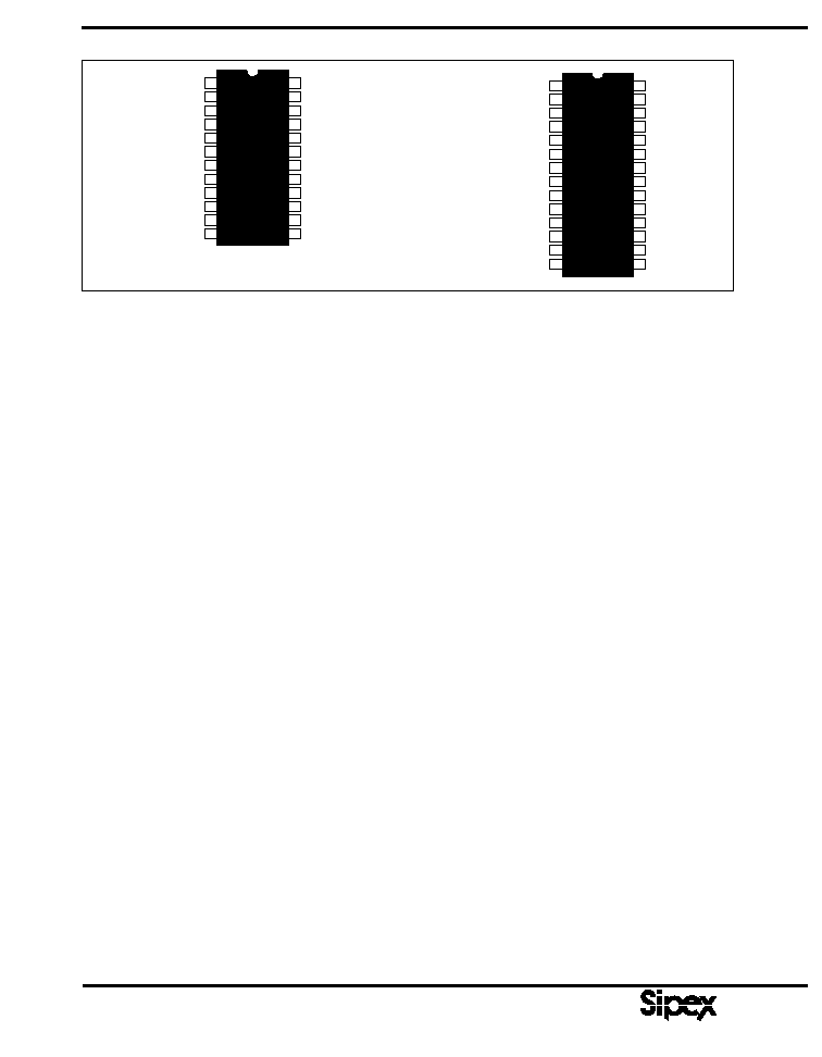
PIN ASSIGNMENTS
SP304CS
V
DD
(+12V) 1
RIA
2
2
RIA
1
3
TOA
2
4
TOA
1
5
SELECT A 6
SELECT B 7
TOB
1
8
TOB
2
9
RIB
1
10
RIB
2
11
GND 12
24 V
CC
(+5V)
23 ROA
2
22 ROA
1
21 TIA
2
20 TIA
1
19 LB
18 N.C.
17 TIB
1
16 TIB
2
15 ROB
1
14 ROB
2
13 V
EE
(-12V)
SP304CT
V
DD
(+12V) 1
RIA
2
2
RIA
1
3
N.C. 4
TOA
2
5
TOA
1
6
SELECT A 7
SELECT B 8
TOB
1
9
TOB
2
10
N.C. 11
RIB
1
12
RIB
2
13
GND 14
28 V
CC
(+5V)
27 ROA
2
26 ROA
1
25 N.C.
24 TIA
2
23 TIA
1
22 LB
21 N.C.
20 TIB
1
19 TIB
2
18 N.C.
17 ROB
1
16 ROB
2
15 V
EE
(-12V)
might result from low amplitude noise voltages
during slower-speed signal transitions.
A loopback test mode is provided that puts the
driver outputs to a high impedance tri-state
level, and routes the driver outputs to their
associated receiver inputs. In this configuration,
the signal path is non-inverting from the TTL
driver input to the receiver TTL output. This
operating mode allows the controlling system to
perform diagnostic self-test of the RS-232/
RS-422 driver/receiver circuitry at speeds up to
3,000 bits per second. In the loopback mode a
±
13.2V input range may be applied to the re-
ceiver inputs with no interference to the loopback
test. In addition, the driver outputs are in a true
high≠impedance state during loopback.
The SP304 is available in 24-pin single width
(0.300") plastic DIP and 28-pin SOIC packages,
for operation over the commercial and indus-
trial temperature ranges.
FEATURES...
The SP304 is a proprietary single-chip device
that contain both RS-232 and RS-422 protocol
line drivers and receivers. It is pin≠for≠pin com-
patible with the Sipex SP302. Like the SP302,
its configuration may be changed at any time by
logic levels on two control lines. In any configu-
ration, the SP304 fully meets the requirements
of both the EIA RS-232D and RS-422 data
communication standards. The SP304 enhance-
ments include improved isolation from external
signals and a true high≠impedance driver output
in the loopback test mode, and no power up
sequence requirements.
The RS-232 line driver circuits convert TTL
logic level inputs into inverted RS-232 output
signals. The RS-422 line drivers convert TTL
logic levels into RS-422 differential output sig-
nals. The RS-422 line driver outputs feature
high source and sink current capability. All line
drivers are internally protected against short
circuits on their outputs.
The RS-232 receivers convert the EIA RS-232
input signals to inverted TTL output logic lev-
els. The RS-422 receivers convert the EIA RS-
422 differential input signals into non-inverted
TTL output logic levels. Receiver input filtering
provides excellent high frequency noise immu-
nity. Input pulses with widths less than 1
µ
s are
completely ignored. The RS-232 receivers have
the additional feature of voltage hysteresis, which
helps eliminate spurious output transitions that
USING THE SP304
POWER SUPPLIES
The SP304 requires
±
12V and +5V for full
RS-232 and RS-422 operation. The
±
12V sup-
plies set up the RS-232
±
9V voltage swings, and
the +5V is used for the internal logic that for-
mats the communications mode and controls the
loopback function. The supply voltages can be
decreased to as low as
±
7V for V
DD
and V
EE
, and
81
Corporation
SIGNAL PROCESSING EXCELLENCE
RIB
1
ROB
1
TOB
1
TIB
1
RIA
1
ROA
1
TOA
1
TIA
1
SELECT A = 1
SELECT B = 0
LOOPBACK = 1
TOA
2
RIA
2
TOB
2
TIB
2
RIB
2
ROB
2
V
DD
GND
V
CC
V
EE
2N2222
V
CC
3.3K
3.3K
Q
3
Q
4
SP304
V
EE
V
DD
Figure 2. Typical Circuit
transmission line with other RS-232 devices
which are not powered by the same power
supplies, it is possible that a device that is not
powered will have a low impedance path to
ground at its driver output. The RS-232 stan-
dards require that with no power applied to the
device, the impedance from a transmitter output
to ground must be greater than 300
. This can
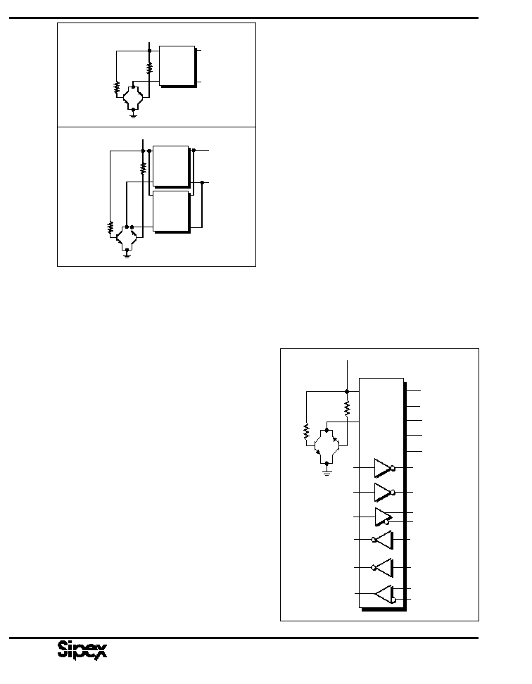
be easily achieved as shown in Figure 1a, where
an external transistor is used as a switch to
isolate an SP304 from ground in the power off
condition. With V
DD
turned on, the transistor
switch is on, connecting ground (GND) for the
device to the circuit ground. In a power-off
condition, this transistor is switched off, thus
isolating the unit from circuit ground, and thereby
leaving the driver in a high impedance state.
Multiple SP304s can be connected as shown in
Figure 1b.
RS-422 OPERATION
The SP304 is a fully compliant RS-422 device
when operating in the RS-422 mode. Baud rate
and drive capability have been balanced to pro-
vide as much versatility as possible. The SP304
is both guaranteed for a 1Mbps data rate,
V
DD
GND
V
CC
V
EE
2N2222
V
EE
V
DD
3.3k
3.3k
Q
3
Q
4
SP304
V
CC
V
DD
GND
V
CC
V
EE
2N2222
V
EE
3.3k
3.3k
V
DD
GND
V
CC
V
EE
Q
3
Q
4
SP304
SP304
V
CC
V
DD
Figure 1. Isolating the SP304 from Ground.
a) Single SP304
b) Multiple SP304
+4.0V for V
CC
. Under these supply conditions,
derated performance can be expected.
POWER SUPPLY SEQUENCING
There are no special power≠up sequencing re-
quirements for the SP304.
GENERAL USAGE
RS-232 Operation
The SP304 is a fully compliant RS-232 device.
Its outputs are fully protected against shorts to
±
20V with no external circuitry. If the potential
exists for momentary shorts to voltages greater
than
±
20V, it is recommended that a 220
resistor be wired in series with each driver
output. This will limit any damage from the
higher short-circuit current from these higher
voltage potentials. Voltage clamps such as back-
to-back Zener diodes can be used to clamp the
driver outputs to "safe" levels. Short circuit
current to ground is internally limited, and can
therefore be sustained infinitely. Under normal
operating conditions, the drivers can typically
source 7mA at
±
5V output, which exceeds the
minimum RS-232 standards requirement.
If an SP304 transmitter output occupies a data

Corporation
SIGNAL PROCESSING EXCELLENCE
82
supplying
±
2V minimum into a 100
load.
Short circuit protection for the RS-422 operat-
ing mode is the same as in the RS-232 mode. The
driver outputs can be shorted to ground for an
infinite duration, with a maximum current of
±
100mA.
The RS-422 receivers accept differential signals
at a 1Mbps rate, and translate them to a non-
inverted TTL output. The receivers are speci-
fied with a
±
15V differential input voltage,
which means that to operate normally, the dif-
ference betweeen the voltages at the inputs
cannot exceed
±
15V. The common mode volt-
age is specified as
±
7V. This identifies the
midpoint of the range about which the differen-
tial input must lie so that the receiver can detect
a change of state. Within this
±
7V range, the
receivers will recognize a change in state with a
±
200mV differential threshold voltage. Since
the RS-232 and RS-422 inputs are shared, all
receiver inputs are protected to
±
30V to guard
against inadvertently applying an RS-232 signal
to an input that is configured for RS-422.
Figure 2 shows a typical circuit for the SP304.
In this case the SP304 is shown configured for
one (1) duplex RS-422 and two (2) duplex
RS-232 communication paths.
CONFIGURING THE SP304
Figures 3, 4 and 5 show the various combina-
tions of simultaneous RS-232 and RS-422
operation that can be achieved with the SP304.
Each of these configurations are software
selectable by logic level on the SELECT A and
SELECT B control lines. Configuration can be
changed "on-the-fly".
83
Corporation
SIGNAL PROCESSING EXCELLENCE
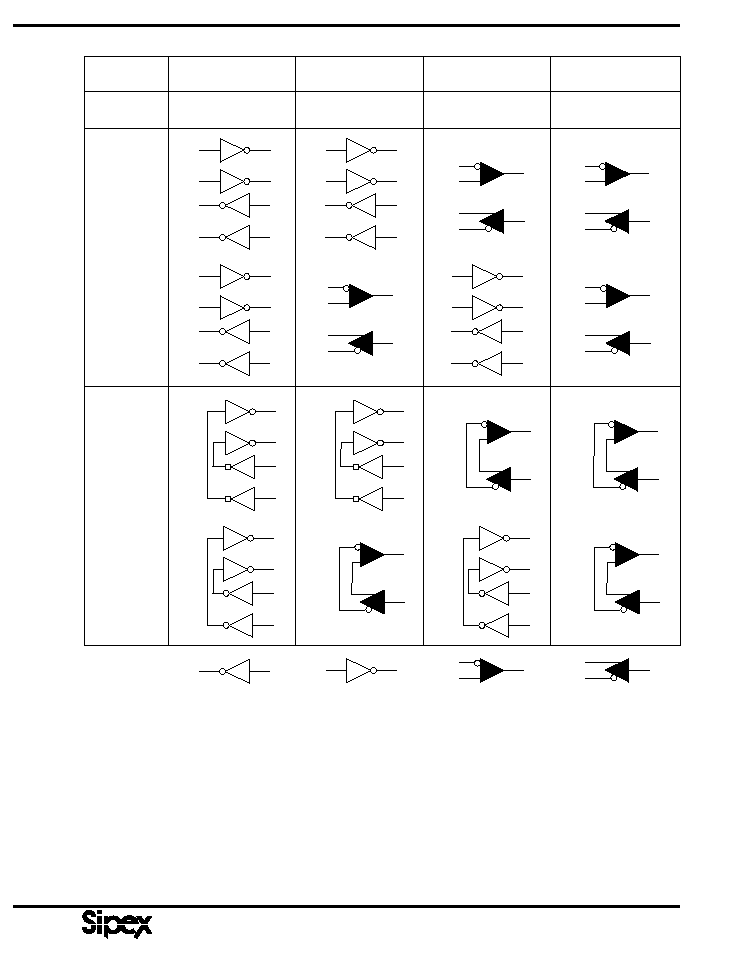
FIGURE 3: SP304 CONTROL LOGIC CONFIGURATION
RIA
1
SELECTION
SELECT A:
SELECT B:
NON≠
LOOPBACK
(LB = 1)
LOOPBACK
(LB=0)
ROA
1
RIB
2
ROB
1
RIB
1
TOB
1
TIB
1
TOB
2
TOA
1
TIA
1
RIA
1
ROA
1
TOA
1
TIA
1
RIA
2
ROA
1
RIA
1
TOA
1
TIA
1
TOA
2
RIA
2
ROA
1
RIA
1
TOA
1
TIA
1
TOA
2
RIB
2
ROB
1
RIB
1
TOB
1
TIB
1
TOB
2
RIB
2
ROB
1
RIB
1
TOB*
1
TIB
1
TOB*
2
RIA
2
ROA
1
RIA
1
TOA*
1
TIA
1
TOA*
2
LOGIC VALUE
1
1
LOGIC VALUE
1
0
LOGIC VALUE
0
1
LOGIC VALUE
0
0
RS-232 DRIVER
* Tri≠state Output
RS-232 RECEIVER
RS-422 RECEIVER
RS-422 DRIVER
RIA
2
ROA
2
RIA
2
ROA
2
TOA
2
TIA
2
TOA
2
TIA
2
RIB
1
ROB
1
TOB
1
TIB
1
RIB
2
ROB
2
TOB
2
TIB
2
RIA
1
ROA
1
TOA*
1
TIA
1
RIA
2
ROA
2
TOA*
2
TIA
2
RIB
1
ROB
1
TOB
1
TIB
1
RIB
2
ROB
2
TOB
2
TIB
2
RIA
1
ROA
1
TOA*
1
TIA
1
RIA
2
ROA
2
TOA*
2
TIA
2
RIB
1
ROB
1
TOB
1
TIB
1
RIB
2
ROB
2
TOB
2
TIB
2
RIB
1
ROB
1
TOB
1
TIB
1
RIB
2
ROB
2
TOB
2
TIB
2
RIA
2
ROA
1
RIA
1
TOA*
1
TIA
1
TOA*
2
RIB
2
ROB
1
RIB
1
TOB*
1
TIB
1
TOB*
2

Corporation
SIGNAL PROCESSING EXCELLENCE
84
Four-Channel Duplex RS-232
Four independent channels of RS-232 line driver
and four channels of RS-232 receiver.
Two-Channel Duplex RS-232 &
One-Channel Duplex RS-422
Two RS-232 line drivers and receivers, and a
single RS-422 line driver and receiver.
FIGURE 4: SP304 CONFIGURATIONS
RIA
1
ROA
1
TOA
1
TIA
1
RIB
1
ROB
1
TOB
1
TIB
1
RS-232 LINE DRIVERS
RS-232 RECEIVERS
RIA
2
ROA
2
TOA
2
TIA
2
RIB
2
ROB
2
TOB
2
TIB
2
SELECT A = 0
SELECT B = 0
LB = 1
RIA
1
ROA
1
TOA
1
TIA
1
RIB
1
ROB
1
TOB
1
TIB
1
RS-422 LINE DRIVER
RS-422 RECEIVER
TOB
2
RIB
2
TOA
2
TIA
2
RIA
2
ROA
2
RS-232 LINE DRIVERS
RS-232 RECEIVERS
SELECT A = 0
SELECT B = 1
LB = 1

85
Corporation
SIGNAL PROCESSING EXCELLENCE
Two-Channel Duplex RS-232 &
One-Channel Duplex RS-422
Opposite Drivers
Two RS-232 line drivers and receivers, and a
single RS-422 line driver and receiver. At first
glance, this is the same configuration as that in
Figure 4. Note however that functions are acti-
vated on the opposite channels.
Two-Channel Duplex RS-422
Two RS-422 line drivers and two RS-422
receivers.
FIGURE 5: SP304 CONFIGURATIONS
RIA
1
ROA
1
TOA
1
TIA
1
RS-422 LINE DRIVERS
RS-422 RECEIVERS
TOA
2
RIA
2
RIB
1
ROB
1
RIB
2
TOB
1
TIB
1
TOB
2
SELECT A = 1
SELECT B = 1
LB = 1
RIB
1
ROB
1
TOB
1
TIB
1
RIA
1
ROA
1
TOA
1
TIA
1
RS-232 LINE DRIVERS
RS-232 RECEIVER
TOA
2
RIA
2
TOB
2
TIB
2
RIB
2
ROB
2
SELECT A = 1
SELECT B = 0
LB = 1
RS-422 LINE DRIVER
RS-422 RECEIVER
Corporation
SIGNAL PROCESSING EXCELLENCE
86
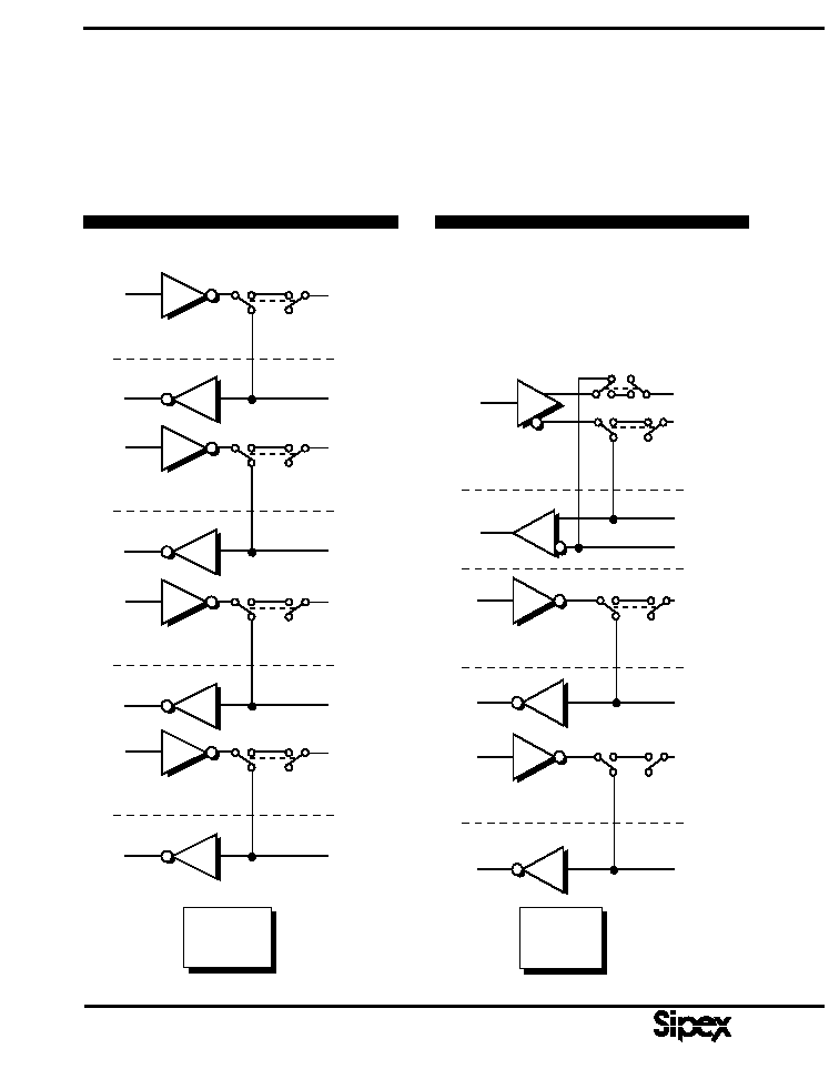
SP304 CONFIGURATIONS IN LOOPBACK MODE
Two -Channel Full Duplex RS-232
One-Channel Full Duplex RS-232 &
One-Channel Full Duplex RS-422
LOOPBACK
The SP304 has a function called loopback, which is
essentially a chip self-test. However, by connecting
system test loops with the inputs and outputs of the
SP304, a system-level diagnostic can be run on
power-up or on command. The test loops can be
RIA
1
ROA
1
TOA
1
TIA
1
RIB
1
ROB
1
TOB
1
TIB
1
RS-232 LINE DRIVER
RS-232 RECEIVER
SELECT A = 0
SELECT B = 0
LB = 0
(ACTIVE)
RIA
2
ROA
2
TOA
2
TIA
2
RIB
2
ROB
2
TOB
2
TIB
2
RS-232 LINE DRIVER
RS-232 RECEIVER
RS-232 LINE DRIVER
RS-232 RECEIVER
RS-232 LINE DRIVER
RS-232 RECEIVER
RIA
1
ROA
1
TOA
1
TIA
1
RIB
1
ROB
1
TOB
1
TIB
1
RS-232 LINE DRIVER
RS-232 RECEIVER
SELECT A = 0
SELECT B = 1
LB = 0
(ACTIVE)
TOB
2
RIB
2
TOA
2
TIA
2
RIA
2
ROA
2
RS-422 LINE DRIVER
RS-422 RECEIVER
RS-232 LINE DRIVER
RS-232 RECEIVER
enabled and disabled allowing both system test and
operation with the same components. A maximum
data rate for loopback of 3kbps is recommended.
Loopback is a pin-programmable function, activated
by a logic low on the LB pin (19). As shown in these
figures, the loopback function internally con-

87
Corporation
SIGNAL PROCESSING EXCELLENCE
SP304 CONFIGURATIONS IN LOOPBACK MODE
One-Channel Full Duplex RS-232 &
One-Channel Full Duplex RS-422
Opposite Drivers
Two-Channel Full Duplex RS-422
RIB
1
ROB
1
TOB
1
TIB
1
RIA
1
ROA
1
TOA
1
TIA
1
RS-232 LINE DRIVERS
RS-232 RECEIVERS
SELECT A = 1
SELECT B = 0
LB = 0
(ACTIVE)
TOA
2
RIA
2
TOB
2
TIB
2
RIB
2
ROB
2
RS-422 LINE DRIVER
RS-422 RECEIVER
RIA
1
ROA
1
TOA
1
TIA
1
RS-422 LINE DRIVERS
RS-422 RECEIVERS
SELECT A = 1
SELECT B = 1
LB = 0
(ACTIVE)
TOA
2
RIA
2
RIB
1
ROB
1
RIB
2
TOB
1
TIB
1
TOB
2
RS-422 LINE DRIVERS
RS-422 RECEIVERS
nects the driver outputs to the corresponding
receiver inputs, and switches the output pin to a
high impedance from V
EE
to ground. Receiver
outputs are left active for signal verification.
During loopback, the receiver inputs are tied to
ground via a 5k
pulldown resistor. The re-
ceiver inputs can accept the full
±
15V swings
with no interference to the loopback function.

Corporation
SIGNAL PROCESSING EXCELLENCE
88
ORDERING INFORMATION
Max # of Duplex Channels
Model
RS-232
RS-422
Temperature
Package
SP304CS .................. 4 ...................... 2 .................................... 0∞C to 70∞C ........................ 24-pin Single-Width Plastic DIP
SP304CT .................. 4 ...................... 2 .................................... 0∞C to 70∞C ....................................................... 28-pin SOIC
SP304ES .................. 4 ...................... 2 .................................. -40∞C to 85∞C ....................... 24-pin Single-Width Plastic DIP
SP304ET .................. 4 ...................... 2 .................................. -40∞C to 85∞C ...................................................... 28-pin SOIC