 | –≠–ª–µ–∫—Ç—Ä–æ–Ω–Ω—ã–π –∫–æ–º–ø–æ–Ω–µ–Ω—Ç: SP320ACF | –°–∫–∞—á–∞—Ç—å:  PDF PDF  ZIP ZIP |
1
Rev:A Date: 1/27/04 SP320 Complete +5V-Only V.35 Interface with RS-232 (V.28) Control Lines © Copyright 2004 Sipex Corporation
14 DRIN1
61 DRA1
59 DRB1
13 T1IN
58 T1OUT
16 T2IN
54 T2OUT
17 T3IN
47 T3OUT
24 T4IN
51 T4OUT
22 DRIN2
42 DRA2
44 DRB2
15 DRIN3
63 DRA3
65 DRB3
23 STEN
6 TTEN
RCA1 70
RCOUT 1
RCB1 71
RCA2 37
RCOUT2 20
RCB2 38
R1IN 66
R1OUT 80
R2IN 68
R2OUT 78
R3IN 35
R3OUT 19
R4IN 39
R4OUT 21
RCA3 76
RCOUT3 79
RTEN 7
RCB3 77
29, 34, 43, 60, 64, 72
VDD
32
26
30
28
31
C1+
C1-
C2+
C2-
27
VSS
VCC
0.1µF
0.1µF
0.1µF
0.1µF
+5V
25, 33, 41, 62, 73
5k
5k
5k
100
100
400k
Vcc
400k
Vcc
400k
Vcc
400k
Vcc
400k
Vcc
400k
Vcc
400k
Vcc
100
3 TS000
9 ENV35
+5V
5k
+
+
+
+
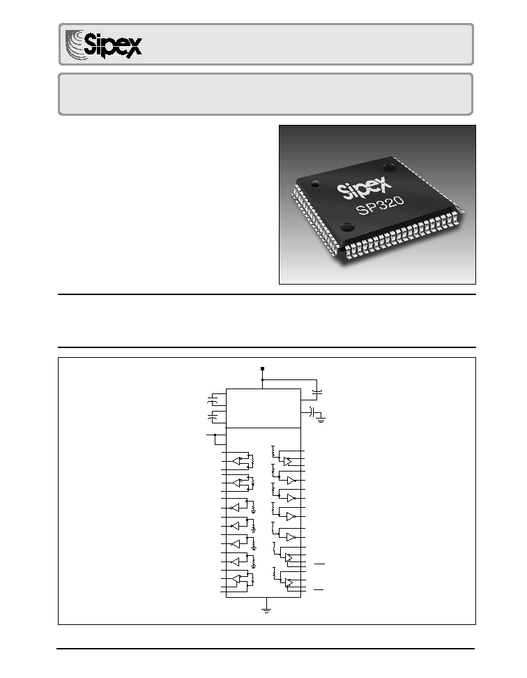
SP320
10Mbps Data Throughput
+5V-Only, Single Supply Operation
3 Drivers, 3 Receivers ≠ V.35
4 Drivers, 4 Receivers ≠ RS-232
80-pin MQFP Surface Mount Packaging
Pin Compatible with SP319
DESCRIPTION
The SP320 is a complete V.35 interface transceiver offering 3 drivers and 3 receivers of V.35, and
4 drivers and 4 receivers of RS-232 (V.28). A Sipex patented charge pump allows +5V only low
power operation. RS-232 drivers and receivers are specified to operate at 120kbps, all V.35
drivers and receivers operate up to 5Mbps.
SP320
Complete +5V-Only V.35 Interface
with RS-232 (V.28) Control Lines
Æ
2
Rev:A Date: 1/27/04 SP320 Complete +5V-Only V.35 Interface with RS-232 (V.28) Control Lines © Copyright 2004 Sipex Corporation
ABSOLUTE MAXIMUM RATINGS
These are stress ratings only and functional operation of the device at
these ratings or any other above those indicated in the operation
sections of the specifications below is not implied. Exposure to absolute
maximum rating conditions for extended periods of time may affect
reliability.
V
CC
.....................................................................................................+7V
Input Voltages
Logic........................................................-0.3V to (V
CC
+0.5V)
Drivers..................................................-0.3V to (V
CC
+0.5V)
Receivers..................................................±30V at 100mA
Output Voltages
Logic........................................................-0.3V to (V
CC
+0.5V)
Drivers.......................................................................±14V
Receivers..............................................-0.3V to (V
CC
+0.5V)
Storage Temperature.......................................................-65∞C to +150∞C
Power Dissipation..........................................................................1500mW
Package Derating
ÿ
JC
.......................................................................16 ∑C/W
ÿ
JA
.......................................................................46 ∑C/W
SPECIFICATIONS
T
MIN
to T
MAX
and V
CC
= 5V±5% unless otherwise noted.
PARAMETER
MIN.
TYP.
MAX.
UNITS
CONDITIONS
V.35 DRIVER
TTL Input Levels
V
IL
0.8
Volts
V
IH
2.0
Volts
Voltage Outputs
Differential Outputs
±0.44
±0.55
±0.66
Volts
R
L
=100 from A to B
Source Impedance
50
100
150
Ohms
Short Circuit Impedance
135
150
165
Ohms
Measured from A=B to Gnd,
V
OUT
=-2V to +2V
Voltage Output Offset
-0.6
+0.6
Volts
V
Offset
={[|V
A
|+|V
B
|]/2}
AC Characteristics
Transition Time
40
ns
Rise/fall time, 10% to 90%
Maximum Transmission Rate
5
Mbps
R
L
=100, V
DIFF OUT
= 0.55V±20%
Propagation Delay
t
PHL
150
250
ns
Measured from 1.5V of V
IN
to 50% of V
OUT
t
PLH
150
250
ns
Measured from 1.5V of V
IN
to 50% of V
OUT
V.35 RECEIVER
TTL Output Levels
V
OL
0.4
Volts
I
OUT
=-3.2mA
V
OH
2.4
Volts
I
OUT
=1.0mA
Receiver Inputs
Differential Input
Threshold
-0.3
+0.3
Volts
Input Impedance
90
100
110
Ohms
Short Circuit Impedance
135
150
165
Ohms
Measured from A=B to Gnd
V
IN
=-2V to +2V
AC Characteristics
Maximum Transmission Rate
5
Mbps
V
IN
= ±0.55V ±20%
Propagation Delay
t
PHL
150
250
ns
Measured from 50% of V
IN
to
1.5V of R
OUT
t
PLH
150
250
ns
Measured from 50% of V
IN
to
1.5V of R
OUT
3
Rev:A Date: 1/27/04 SP320 Complete +5V-Only V.35 Interface with RS-232 (V.28) Control Lines © Copyright 2004 Sipex Corporation
SPECIFICATIONS (CONTINUED)
T
MIN
to T
MAX
and V
CC
= 5V±5% unless otherwise noted.
PARAMETER
MIN.
TYP.
MAX.
UNITS
CONDITIONS
RS-232 DRIVER
TTL Input Levels
V
IL
0.8
Volts
V
IH
2.0
Volts
Voltage Outputs
High Level Output
+5.0
+15.0
Volts
R
L
= 3k to Gnd
Low Level Output
-15.0
-5.0
Volts
R
L
= 3k to Gnd
Open Circuit Output
-15
+15
Volts
R
L
=
Short Circuit Current
-100
+100
mA
R
L
= Gnd
Power Off Impedance
300
Ohms
V
CC
= 0V; V
OUT
= ±2V
AC Characteristics
Slew Rate
30
V/µs
R
L
= 3k, C
L
= 50pF; From +3V to -3V
or -3V to +3V, T
A
= 25∞C, V
CC
= +5V
Maximum Transmission Rate
120
kbps
R
L
= 3k, C
L
= 2500pF
Transition Time
1.56
µs
Rise/fall time, between ±3V
R
L
= 3k, C
L
= 2500pF
Propagation Delay
t
PHL
2
8
µs
R
L
= 3k, C
L
= 2500pF; From 1.5V
of T
IN
to 50% of V
OUT
t
PLH
2
8
µs
R
L
= 3k, C
L
= 2500pF; From 1.5V
of T
IN
to 50% of V
OUT
RS-232 RECEIVER
TTL Output Levels
V
OL
0.4
Volts
V
OH
2.4
Volts
Receiver Input
Input Voltage Range
-15
+15
Volts
High Threshold
1.7
3.0
Volts
Low Threshold
0.8
1.2
Volts
Hysteresis
0.2
0.5
1
Volts
V
CC
= 5V; T
A
= +25∞C
Receiver Input Circuit Bias
+2.0
Volts
Input Impedance
3
5
7
kOhms
V
IN
= ±15V
AC Characteristics
Maximum Transmission Rate
120
kbps
Propagation Delay
t
PHL
0.1
1
µs
From 50% of R
IN
to 1.5V of R
OUT
t
PLH
0.1
1
µs
From 50% of R
IN
to 1.5V of R
OUT
POWER REQUIREMENTS
No Load V
CC
Supply Current
35
70
mA
No load; V
CC
= 5.0V; T
A
= 25∞C
Full Load V
CC
Supply Current
60
mA
RS-232 drivers R
L
= 3k to Gnd;
DC Input
V.35 drivers R
L
= 100 from A to B;
DC Input
Shutdown Current
1.5
mA
TS000 = ENV35 = 0V

4
Rev:A Date: 1/27/04 SP320 Complete +5V-Only V.35 Interface with RS-232 (V.28) Control Lines © Copyright 2004 Sipex Corporation
All of the V.35 receivers can operate at data
rates as high as 5Mbps. The sensitivity of the
V.35 receiver inputs is
±300mV.
RS-232 (V.28) Drivers
The RS-232 drivers are inverting transmitters,
which accept either TTL or CMOS inputs and
output the RS-232 signals with an inverted sense
relative to the input logic levels. Typically, the
RS-232 output voltage swing is
±9V with no
load, and
±5V minimum with full load. The
transmitter outputs are protected against infinite
short-circuits to ground without degradation in
reliability.
In the power off state, the output impedance of
the RS-232 drivers will be greater than 300
over a
±2V range. Should the input of a driver be
left open, an internal 400k
pullup resistor to
V
CC
forces the input high, thus committing the
output to a low state. The slew rate of the
transmitter output is internally limited to a
maximum of 30V/
µs in order to meet the EIA
standards. The RS-232 drivers are rated for
120kbps data rates.
RS-232 (V.28) Receivers
The RS-232 receivers convert RS-232 input
signals to inverted TTL signals. Each of the four
receivers features 500mV of hysteresis margin
to minimize the effects of noisy transmission
lines. The inputs also have a 5k
resistor to
ground; in an open circuit situation the input of
the receiver will be forced low, committing the
output to a logic high state. The input resistance
will maintain 3k
-7k over a ±15V range.
The maximum operating voltage range for the
receiver is
±30V, under these conditions the
input current to the receiver must be limited to
less than 100mA. The RS-232 receivers can
operate to beyond 120kbps.
CHARGE PUMP
The charge pump is a Sipex patented design
(U.S. 5,306,954) and uses a unique approach
compared to older less-efficient designs. The
charge pump still requires four external
capacitors, but uses a four-phase voltage
shifting technique to attain symmetrical
±10V
power supplies. The capacitors can be as low
as 0.1
µF with a 16 Volt rating. Polarized or
non-polarized capacitors can be used.
THEORY OF OPERATION
The SP320 is a single chip +5V-only serial
transceiver that supports all the signals neces-
sary to implement a full V.35 interface. Three
V.35 drivers and three V.35 receivers make up
the clock and data signals. Four RS-232 (V.28)
drivers and four RS-232 (V.28) receivers are
used for control line signals for the interface.
V.35 Drivers
The V.35 drivers are +5V-only, low power
voltage output transmitters. The drivers do not
require any external resistor networks, and will
meet the following requirements:
1. Source impedance in the range of 50
to
150
.
2. Resistance between short-circuited terminals
and ground is 150
±15.
3. When terminated with a 100
resistive load
the terminal to terminal voltage will be 0.55
Volts
±20% so that the A terminal is positive to
the B terminal when binary 0 is transmitted, and
the conditions are reversed to transmit binary 1.
4. The arithmetic mean of the voltage of the A
terminal with respect to ground, and the B
terminal with respect to ground will not exceed
0.6 Volts when terminated as in 3 above.
The V.35 drivers can operate at data rates as
high as 5Mbps. The driver outputs are protected
against short-circuits between the A and B
outputs and short circuits to ground.
Two of the V.35 drivers, DRIN2 and DRIN3 are
equipped with enable control lines. When the
enable pins are high the driver outputs are
disabled, the output impedance of a disabled
driver will nominally be 300
. When the enable
pins are low, the drivers are active.
V.35 Receivers
The V.35 receivers are +5V only, low power
differential receivers which meet the following
requirements:
1. Input impedance in the range of 100
±10.
2. Resistance to ground of 150
±15,
measured from short-circuited terminals.

5
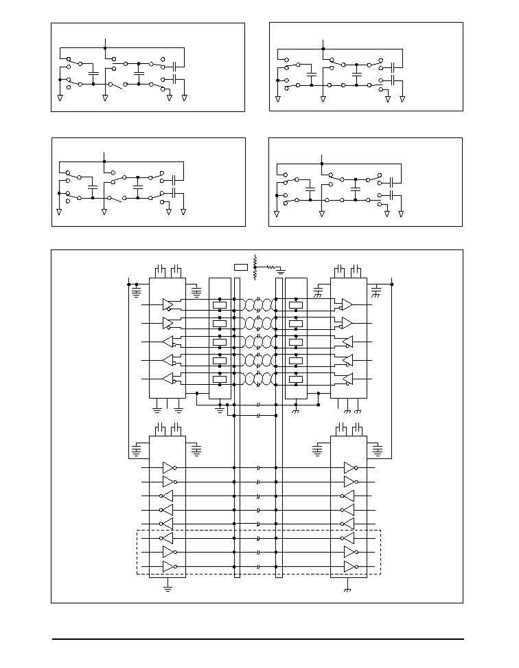
Rev:A Date: 1/27/04 SP320 Complete +5V-Only V.35 Interface with RS-232 (V.28) Control Lines © Copyright 2004 Sipex Corporation
Phase 4
-Vdd transfer- The fourth phase of the clock
connects the negative terminal of C2 to ground
and transfers the generated +10V across C2 to
C4, the Vdd storage capacitor. Again, simulta-
neously with this, the positive side of capacitor
C1 is switched to +5V and the negative side is
connected to ground, and the cycle begins again.
Since both V+ and V- are separately generated
from Vcc in a no load condition, V+and V- will
be symmetrical. Older charge pump approaches
that generate V- from V+ will show a decrease
in the magnitude of V- compared to V+ due to
the inherent inefficiencies in the design.
The clock rate for the charge pump typically
operates at 15kHz. The external capacitors must
be 0.1
µF with a 16V breakdown rating.
Shutdown Mode
The SP320 can be put into a low power
shutdown mode by bringing both TS000 (pin 3)
and ENV35 (pin 9) low. In shutdown mode, the
SP320 will draw less than 2mA of supply
current. For normal operation, both pins should
be connected to +5V.
External Power Supplies
For applications that do not require +5V only,
external supplies can be applied at the V+ and
V- pins. The value of the external supply
voltages must be no greater than
±10V. The
current drain from the
±10V supplies is used for
the RS-232 drivers. For the RS-232 driver the
current requirement will be 3.5mA per driver.
It is critical the external power supplies provide
a power supply sequence of : +10V, +5V, and
then -10V.
Applications Information
The SP320 is a single chip device that can
implement a complete V.35 interface. Three (3)
V.35 drivers and three (3) V.35 receivers are
used for clock and data signals and four (4)
RS-232 (V.28) drivers and four (4) RS-232
(V.28) receivers can be used for the control
signals of the interface. The following examples
show the SP320 configured in either a DTE or
DCE application.
+10V
a) C
2
+
GND
GND
b) C
2
≠
≠10V
Figure 1. Charge Pump Waveforms
Figure 1a shows the waveform found on the
positive side of capacitor C2, and Figure 1b
shows the negative side of capacitor C2. There
is a free-running oscillator that controls the four
phases of the voltage shifting. A description of
each phase follows.
Phase 1
-Vss charge storage- During this phase of the
clock cycle, the positive side of capactors C1
and C2 are initially charged to +5V. C1+ is then
switched to ground and the charge in C1- is
transferred to C2-. Since C2+ is connected to
+5V, the voltage potential across capacitor C2 is
now 10V.
Phase 2
-Vss transfer- Phase two of the clock connects
the negative terminal of C2 to the Vss storage
capacitor and the positive terminal of C2 to
ground, and transfers the generated -10V to C3.
Simultaneously, the positive side of capacitor
C1 is switched to +5V and the negative side is
connected to ground.
Phase 3
-Vdd charge storage- The third phase of the
clock is identical to the first phase- the trans-
ferred charge in C1 produces -5V in the negative
terminal of C1, which is applied to the negative
side of capacitor C2. Since C2+ is at +5V, the
voltage potential across C2 is +10V.
6
Rev:A Date: 1/27/04 SP320 Complete +5V-Only V.35 Interface with RS-232 (V.28) Control Lines © Copyright 2004 Sipex Corporation
Figure 2. Charge Pump Phase 1
Figure 3. Charge Pump Phase 2
V
CC
= +5V
+10V
V
SS
Storage Capacitor
V
DD
Storage Capacitor
C
1
C
2
C
3
C
4
+
+
+
+
≠
≠
≠
≠
V
CC
= +5V
≠5V
≠5V
+5V
V
SS
Storage Capacitor
V
DD
Storage Capacitor
C
1
C
2
C
3
C
4
+
+
+
+
≠
≠
≠
≠
Figure 4. Charge Pump Phase 3
Figure 5. Charge Pump Phase 4
V
CC
= +5V
≠10V
V
SS
Storage Capacitor
V
DD
Storage Capacitor
C
1
C
2
C
3
C
4
+
+
+
+
≠
≠
≠
≠
V
CC
= +5V
≠5V
+5V
≠5V
V
SS
Storage Capacitor
V
DD
Storage Capacitor
C
1
C
2
C
3
C
4
+
+
+
+
≠
≠
≠
≠
Figure 6. A Competitor's Typical V.35 Solution Using Six Components.
1µF
1µF
1µF
1µF
DX
T
P
S
TXD (103)
RX
T
P
S
DX
T
U
W
SCTE (113)
RX
T
U
W
T
AA
Y
TXC (114)
DX
T
Y
T
X
V
RXC (115)
T
X
V
RX
T
T
R
TXD (104)
T
T
R
RX
RX
DX
DX
AA
T
=
50
50 125
1µF
1µF
V
CC2
B
A
GND (102)
CABLE SHIELD
B
A
V
CC1
1µF
1µF
DX
DX
RX
RX
RX
RX
DX
DX
1µF
1µF
1µF
1µF
RX
RX
DX
DX
DX
DX
RX
RX
1µF
1µF
ISO 2593
34-PIN DTE/DCE
INTERFACE
CONNECTOR
ISO 2593
34-PIN DTE/DCE
INTERFACE
CONNECTOR
V.35
V.35
RS-232
RS-232
H
DTR (108)
H
C
RTS (105)
C
E
DSR (107)
E
D
CTS (106)
D
F
DCD (109)
F
NN
TM (142)
N
RDL (140)
N
L
LLB (141)
L
NN
OPTIONAL
SIGNALS
V
CC1
5V
V
CC2
5V
7
Rev:A Date: 1/27/04 SP320 Complete +5V-Only V.35 Interface with RS-232 (V.28) Control Lines © Copyright 2004 Sipex Corporation
0.1µF
25
27 26 30
32
1N5819
V
CC
V
DD
C1-
C2-
V
SS
C1+
C2+
0.1µF
SP320CF
14
79
28
31
0.1µF
+5V
15
20
1
22
0.1µF
0.1µF
25
27 26 30
32
1N5819
V
CC
V
DD
C1-
C2-
V
SS
C1+
C2+
0.1µF
SP320CF
28
31
0.1µF
+5V
0.1µF
RC
OUT
1
14
20
79
22
15
14
TxD (103)
TxC (113)
TxCC (114)
RxC (115)
RxD (104)
DTR (108)
RTS (105)
RL (140)
LL (141)
DSR (107)
CTS (106)
DCD (109)
TM (142)
78
R1
OUT
80
R4
OUT
21
RC
OUT
2
RC
OUT
3
DR
IN
2
DR
IN
3
DR
IN
1
R2
OUT
R3
OUT
19
T2
IN
16
T1
IN
13
T3
IN
17
T4
IN
24
DR
IN
1
DR
IN
3
DR
IN
2
RC
OUT
3
RC
OUT
2
RC
OUT
1
T2
IN
16
T1
IN
13
T3
IN
17
T4
IN
24
R2
OUT
78
R1
OUT
80
R3
OUT
19
R4
OUT
21
P
S
U
W
Y
AA
X
V
T
R
H
C
N
L
E
D
F
NN
P
S
U
W
Y
AA
X
V
T
R
H
C
L
E
D
F
N
NN
29, 34, 43, 60, 64, 72
29, 34, 43, 60, 64, 72
B
B
A
A
ISO2593
34-PIN DTE/DCE
INTERFACE CONNECTOR
ISO2593
34-PIN DTE/DCE
INTERFACE CONNECTOR
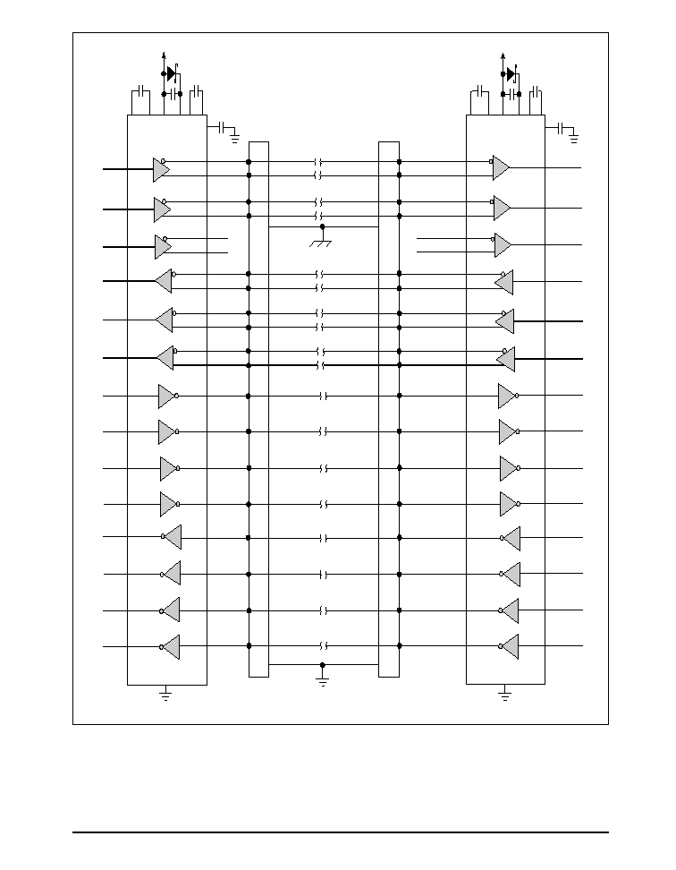
Figure 7. Typical DTE-DCE V.35 Connection with the SP320
8
Rev:A Date: 1/27/04 SP320 Complete +5V-Only V.35 Interface with RS-232 (V.28) Control Lines © Copyright 2004 Sipex Corporation
14 DRIN1
61 DRA1
59 DRB1
13 T1IN
58 T1OUT
16 T2IN
54 T2OUT
17 T3IN
47 T3OUT
24 T4IN
51 T4OUT
22 DRIN2
42 DRA2
44 DRB2
15 DRIN3
63 DRA3
65 DRB3
23 STEN
6 TTEN
RCA1 70
RCOUT 1
RCB1 71
RCA2 37
RCOUT2 20
RCB2 38
R1IN 66
R1OUT 80
R2IN 68
R2OUT 78
R3IN 35
R3OUT 19
R4IN 39
R4OUT 21
RCA3 76
RCOUT3 79
RTEN 7
RCB3 77
RXD
104(A)
104(B)
CTS
106
DSR
107
DCD
109
RI
125
RXC
115(A)
115(B)
TXCC
114(A)
114(B)
103(A)
103(B)
TXD
113(A)
TXC
113(B)
RTS
105
DTR
108
RLPBK
140
LLPBK
141
SPARE
SPARE
SPARE
29, 34, 43, 60, 64, 72
VDD
32
26
30
28
31
C1+
C1-
C2+
C2-
27
VSS
VCC
0.1µF
0.1µF
0.1µF
0.1µF
+5V
25, 33, 41, 62, 73
5k
5k
5k
100
100
400K
Vcc
400k
Vcc
400k
Vcc
400k
Vcc
400k
Vcc
400k
Vcc
400k
Vcc
100
3 TS000
9 ENV35
+5V
5k
+
+
+
+
A
Chasis Ground
C
Request to Send
E
DCE Ready (DSR)
H
DTE Ready (DTR)
K
Unassigned---
M
Unassigned---
P
Transmitted Data (A)
S
Transmitted Data (B)
U
Terminal Timing (A) } 113(A)
W
Terminal Timing (B) } 113(B)
Y
Transmit Timing (A) } 114(A)
AA
Transmit Timing (B) } 114(B)
CC
Unassigned---
EE
Unassigned---
HH
Unassigned---
KK
Unassigned---
MM
Unassigned---
Signal Ground
B
Clear to Send
D
Data Carrier Detect
F
Ring Indicator
J
Local Loopback
L
Remote Loopback
N
Receive Data (A)
R
Receive Data (B)
T
Receive Timing (A)
V
Receive Timing (B)
X
Unassigned---
Z
Unassigned---
BB
Unassigned---
DD
Unassigned---
FF
Unassigned---
JJ
Unassigned---
LL
Test Mode
NN
ISO-2593 connector pin out
Typical DCE V.35 interface
SP320
9
Rev:A Date: 1/27/04 SP320 Complete +5V-Only V.35 Interface with RS-232 (V.28) Control Lines © Copyright 2004 Sipex Corporation
14 DRIN1
61 DRA1
59 DRB1
13 T1IN
58 T1OUT
16 T2IN
54 T2OUT
17 T3IN
47 T3OUT
24 T4IN
51 T4OUT
22 DRIN2
42 DRA2
44 DRB2
15 DRIN3
63 DRA3
65 DRB3
23 STEN
6 TTEN
RCA1 70
RCOUT 1
RCB1 71
RCA2 37
RCOUT2 20
RCB2 38
R1IN 66
R1OUT 80
R2IN 68
R2OUT 78
R3IN 35
R3OUT 19
R4IN 39
R4OUT 21
RCA3 76
RCOUT3 79
RTEN 7
RCB3 77
29, 34, 43, 60, 64, 72
VDD
32
26
30
28
31
C1+
C1-
C2+
C2-
27
VSS
VCC
0.1µF
0.1µF
0.1µF
0.1µF
+5V
25, 33, 41, 62, 73
5k
5k
5k
100
100
400k
Vcc
400k
Vcc
400k
Vcc
400k
Vcc
400k
Vcc
400k
Vcc
400k
Vcc
100
3 TS000
9 ENV35
+5V
TXD
103(A)
103(B)
RTS
105
DTR
108
RLPBK
140
LLPBK
141
SPARE
SPARE
SPARE
TXCT
113(A)
113(B)
104(A)
104(B)
RXD
114(A)
TXCC
114(B)
106
CTS
107
DSR
109
DCD
125
RI
115(A)
RXC
115(B)
5k
+
+
+
+
A
Chasis Ground
C
Request to Send
E
DCE Ready (DSR)
H
DTE Ready (DTR)
K
Unassigned---
M
Unassigned---
P
Transmitted Data (A)
S
Transmitted Data (B)
U
Terminal Timing (A) } 113(A)
W
Terminal Timing (B) } 113(B)
Y
Transmit Timing (A) } 114(A)
AA
Transmit Timing (B) } 114(B)
CC
Unassigned---
EE
Unassigned---
HH
Unassigned---
KK
Unassigned---
MM
Unassigned---
Signal Ground
B
Clear to Send
D
Data Carrier Detect
F
Ring Indicator
J
Local Loopback
L
Remote Loopback
N
Receive Data (A)
R
Receive Data (B)
T
Receive Timing (A)
V
Receive Timing (B)
X
Unassigned---
Z
Unassigned---
BB
Unassigned---
DD
Unassigned---
FF
Unassigned---
JJ
Unassigned---
LL
Test Mode
NN
ISO-2593 connector pin out
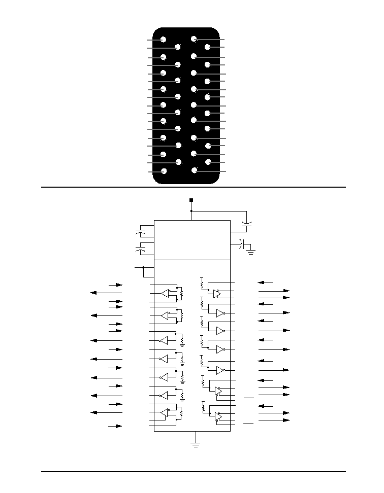
Typical DTE V.35 interface
SP320
10
Rev:A Date: 1/27/04 SP320 Complete +5V-Only V.35 Interface with RS-232 (V.28) Control Lines © Copyright 2004 Sipex Corporation
14 DRIN1
61 DRA1
59 DRB1
13 T1IN
58 T1OUT
16 T2IN
54 T2OUT
17 T3IN
47 T3OUT
24 T4IN
51 T4OUT
22 DRIN2
42 DRA2
44 DRB2
15 DRIN3
63 DRA3
65 DRB3
23 STEN
6 TTEN
RCA1 70
RCOUT 1
RCB1 71
RCA2 37
RCOUT2 20
RCB2 38
R1IN 66
R1OUT 80
R2IN 68
R2OUT 78
R3IN 35
R3OUT 19
R4IN 39
R4OUT 21
RCA3 76
RCOUT3 79
RTEN 7
RCB3 77
29, 34, 43, 60, 64, 72
VDD
32
26
30
28
31
C1+
C1-
C2+
C2-
27
VSS
VCC
0.1µF
0.1µF
0.1µF
0.1µF
+5V
25, 33, 41, 62, 73
5k
5k
5k
100
100
400k
Vcc
400k
Vcc
400k
Vcc
400k
Vcc
400k
Vcc
400k
Vcc
400k
Vcc
100
3 TS000
9 ENV35
+5V
5k
+
+
+
+
60 GND
59 DRB1
58 T1OUT
57 NC
56 NC
55 NC
54 T2OUT
53 NC
52 NC
51 T4OUT
50 NC
49 NC
48 NC
47 T3OUT
46 NC
45 NC
44 DRB2
43 GND
42 DRA2
41 VCC
80 R1OUT
79 RCOUT3
78 R2OUT
77 RCB3
76 RCA3
75 NC
74 NC
73 VCC
72 GND
71 RCB1
70 RCA1
69 NC
68 R2IN
67 NC
66 R1IN
65 DRB3
64 GND
63 DRA3
62 VCC
61 DRA1
ROUT4 21
DRIN2 22
T4IN 24
VCC 25
C1+ 26
VDD 27
C2+ 28
GND 29
C1- 30
C2- 31
VSS 32
VCC 33
GND 34
R3IN 35
NC 36
RCA2 37
RCB2 38
R4IN 39
NC 40
STEN 23
RCOUT1 1
NC 2
TS000 3
NC 4
NC 5
TTEN 6
RTEN 7
NC 8
ENV35 9
NC 10
NC 11
NC 12
T1IN 13
DRIN1 14
DRIN3 15
T2IN 16
T3IN 17
NC 18
R3OUT 19
RCOUT2 20
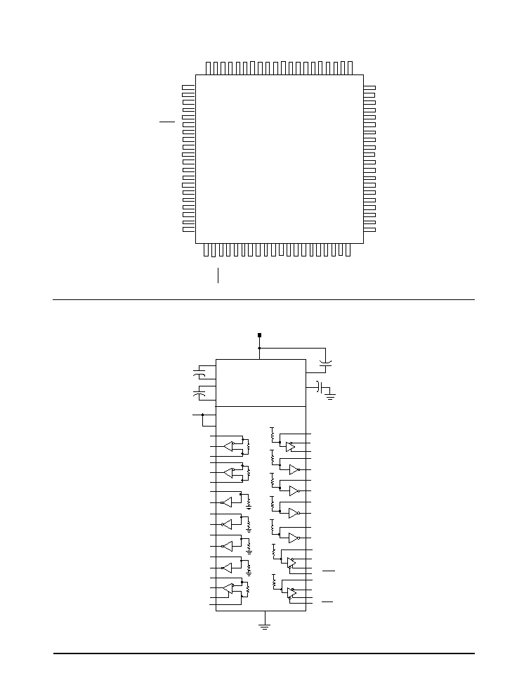
Pin configuration
SP320
Typical application circuit
SP320
11
Rev:A Date: 1/27/04 SP320 Complete +5V-Only V.35 Interface with RS-232 (V.28) Control Lines © Copyright 2004 Sipex Corporation
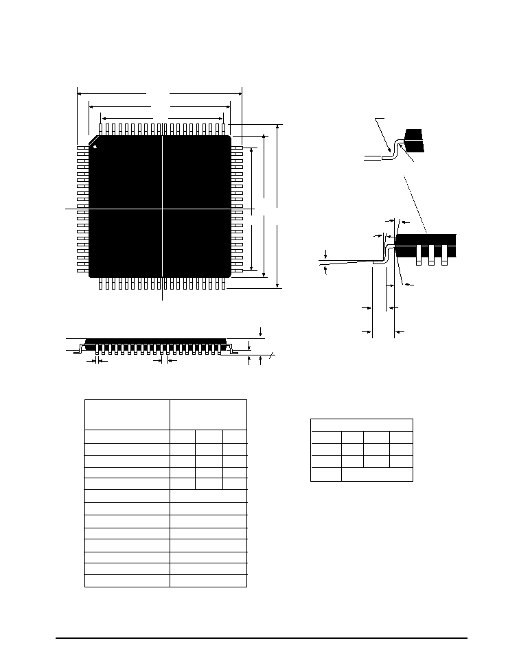
PACKAGE: 80 Pin MQFP
80 PIN MQFP (MS-022 BC)
b
e
Seating
Plane
A1
A
A
L1
5∞-16∞
0∞ MIN.
0∞≠7∞
5∞-16∞
L
A2
0.30" RAD. TYP.
0.20" RAD. TYP.
c
PIN 1
E1
D1
D
CL
E
CL
D2
E2
DIMENSIONS
Minimum/Maximum
(mm)
SYMBOL
A
A1
A2
b
D
D1
D2
E
E1
E2
e
N
80≠PIN MQFP
JEDEC MS-22
(BEC) Variation
MIN
NOM
MAX
2.45
0.00
0.25
1.80
2.00
2.20
0.22
0.40
17.20 BSC
14.00 BSC
12.35 REF
17.20 BSC
14.00 BSC
12.35 REF
0.65 BSC
80
COMMON DIMENTIONS
SYMBL MIN
NOM
MAX
c
0.11
23.00
L
0.73
0.88
1.03
L1
1.60 BASIC
12
Rev:A Date: 1/27/04 SP320 Complete +5V-Only V.35 Interface with RS-232 (V.28) Control Lines © Copyright 2004 Sipex Corporation
ORDERING INFORMATION
Model
Temperature Range
Package Types
SP320ACF ................................................... 0∞C to +70∞C ...................... 80-pin JEDEC (BE-2 Outline) MQFP
Please consult the factory for pricing and availability on a Tape-On-Reel option.
Sipex Corporation reserves the right to make changes to any products described herein. Sipex does not assume any liability arising out of the
application or use of any product or circuit described herein; neither does it convey any license under its patent rights nor the rights of others.
DATE
REVISION
DESCRIPTION
1/27/04
A
Implemented tracking revision.
REVISION HISTORY