 | –≠–ª–µ–∫—Ç—Ä–æ–Ω–Ω—ã–π –∫–æ–º–ø–æ–Ω–µ–Ω—Ç: SP4490EU | –°–∫–∞—á–∞—Ç—å:  PDF PDF  ZIP ZIP |
Rev. 9/12/00
SP4490 Two Panel Electroluminescent Lamp Driver
© Copyright 2000 Sipex Corporation
1
s
Single IC Drives 2 EL Lamps
Independently For Backlighting:
∑
Cell Phone Keypad & LCD
∑
Multi-Color EL Lamps
∑
Multi-Segment EL Lamps
s
Control Over Lamp-A & Lamp-B For
Independent Operation
s
+2.2V to +6.0V Battery Operation
s
Single Coil Used To Generate High
Voltage AC Outputs
s
Low Power Standby Mode Draws 100nA
Typical Current
s
A Single Resistor Controls the Internal
Oscillator
s
DC-AC Inverter Produces Up To 220V
PP
s
Space-Saving 10
µ
SOIC Package
DESCRIPTION
The SP4490 electroluminescent lamp driver provides designers of cell phones PDA's and
other handheld, portable electronic devices with an integrated solution for driving two EL
lamps independently. The SP4490 reduces system cost, component count and board space
requirements over a discrete 2-EL driver approach. The EL lamps operate in opposite phase
so the SP4490 can be easily implemented in applications driving multi-color or multi-segment
EL lamps. The SP4490 operates from a +2.2V to +6.0V battery source. The device features
a low power standby mode which draws less than 1
µ
A. The frequency of the internal oscillator
is set using a single external resistor. A single external inductor is required to generate the
high voltage AC outputs to drive the EL lamps. All input pins are ESD protected with internal
diodes to V
DD
and V
SS
.
R
OSC
V
DD
ELcommon
EL1
1
2
3
4
7
8
9
10
V
SS
5
EL2
COIL
6
CAP
SP4490
EL1/EL2
ON/OFF
SP4490
Two Panel Electroluminscent Lamp Driver
APPLICATIONS
s
Cellular Phones
s
PDA's
s
Handheld GPS Units
s
Security Systems
s
POS Terminals
Æ
Rev. 9/12/00
SP4490 Two Panel Electroluminescent Lamp Driver
© Copyright 2000 Sipex Corporation
2
ABSOLUTE MAXIMUM RATINGS
These are stress ratings only and functional operation of
the device at these ratings or any other above those
indicated in the operation sections of the specifications
below is not implied. Exposure to absolute maximum
rating conditions for extended periods of time may affect
reliability.
Power Supply, V
DD
.................................................7.0V
Input Voltages, Logic.....................-0.3V to (V
DD
+0.3V)
Lamp Outputs...................................................220V
P-P
Operating Temperature.........................-40∞C to +85∞C
Storage Temperature..........................-65∞C to +150∞C
Power Dissipation Per Package
10-pin
µ
SOIC
(derate 8.84mW/∞C above +70∞C)....................720mW
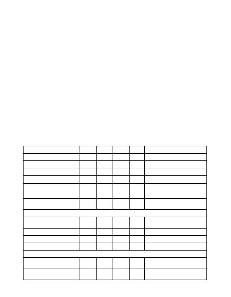
SPECIFICATIONS
V
DD
= +3.0V, L = 470
µ
H, C
LAMP
= 8nF, R
OSC
= 464k
, and T
AMB
= 25∞C unless otherwise noted.
STORAGE CONSIDERATIONS
Storage in a low humidity environment is pre-
ferred. Large high density plastic packages are
moisture sensitive and should be stored in Dry
Vapor Barrier Bags. Prior to usage, the parts
should remain bagged and stored below 40
∞
C and
60%RH. If the parts are removed from the bag,
they should be used within 48 hours or stored in an
environment at or below 20%RH. If the above
conditions cannot be followed, the parts should be
baked for four hours at 125
∞
C in order remove
moisture prior to soldering. Sipex ships product in
Dry Vapor Barrier Bags with a humidity indicator
card and desiccant pack. The humidity indicator
should be below 30%RH.
R
E
T
E
M
A
R
A
P
.
N
I
M
.
P
Y
T
.
X
A
M
S
T
I
N
U
S
N
O
I
T
I
D
N
O
C
V
,
e
g
a
t
l
o
V
y
l
p
p
u
S
D
D
2
.
2
0
.
3
0
.
6
V
I
,
t
n
e
r
r
u
C
y
l
p
p
u
S
D
D
4
.
1
0
.
4
A
m
L
L
I
O
C
0
7
4
=
µ
H
V
,
e
g
a
t
l
o
V
li
o
C
L
I
O
C
V
D
D
V
I
,
t
n
e
r
r
u
C
n
w
o
d
t
u
h
S
D
S
I
=
L
I
O
C
I
+
D
D
1
µ
A
V
N
E
L
E
V
0
=
V
,
e
g
a
t
l
o
V
t
u
p
n
I
N
E
L
E
N
E
L
E
W
O
L
H
G
I
H
5
7
.
2
0
0
.
3
5
2
.
0
V
e
c
n
a
t
s
i
s
e
R
t
u
p
n
I
F
F
O
/
N
O
d
n
a
2
L
E
/
1
L
E
1
M
E
V
I
R
D
R
O
T
C
U
D
N
I
f
,
y
c
n
e
u
q
e
r
F
li
o
C
L
I
O
C
5
4
0
4
7
5
0
7
3
7
z
H
k
T
B
M
A
5
2
+
=
O
C
T
B
M
A
0
4
-
=
O
5
8
+
o
t
C
O
C
e
l
c
y
C
y
t
u
D
li
o
C
0
9
%
I
,
t
n
e
r
r
u
C
li
o
C
L
I
O
C
9
3
0
6
A
m
I
,
t
n
e
r
r
u
C
li
o
C
k
a
e
P
L
I
O
C
-
K
P
4
7
0
0
1
A
m
n
g
i
s
e
d
y
b
d
e
e
t
n
a
r
a
u
G
T
U
P
T
U
O
P
M
A
L
L
E
f
,
y
c
n
e
u
q
e
r
F
p
m
a
L
L
E
P
M
A
L
0
5
3
2
1
3
0
5
4
0
5
5
0
7
5
z
H
T
B
M
A
5
2
+
=
O
C
T
B
M
A
0
4
-
=
O
5
8
+
o
t
C
O
C
V
,
e
g
a
t
l
o
V
t
u
p
t
u
O
k
a
e
P
o
t
k
a
e
P
K
P
-
K
P
8
3
1
0
3
1
0
7
1
V
T
B
M
A
5
2
+
=
O
C
T
B
M
A
0
4
-
=
O
5
8
+
o
t
C
O
C
The information furnished by Sipex has been care-
fully reviewed for accuracy and reliability. Its applica-
tion or use, however, is solely the responsibility of the
user. No responsibility for the use of this information
become part of the terms and conditions of any
subsequent sales agreement with Sipex. Specifica-
tions are subject to change without no responsibility
for any infringement of patents or other rights of third
parties which may result from its use. No license or
other proprietary rights are granted by implication or
otherwise under any patent or patent rights of Sipex
Corporation.
Rev. 9/12/00
SP4490 Two Panel Electroluminescent Lamp Driver
© Copyright 2000 Sipex Corporation
3
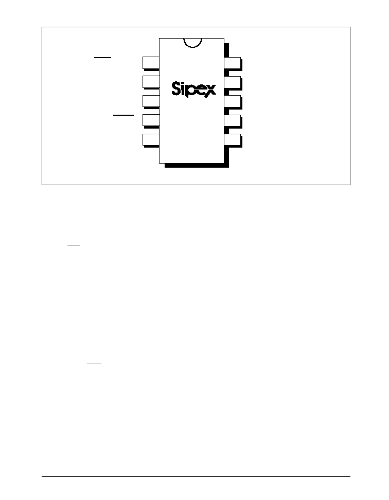
PIN ASSIGNMENTS
Pin 1 -- EL1/EL2 -- Electroluminescent Lamp
Output Select. Selects either EL1 Output
when input is LOW or EL2 Output when
input is HIGH.
Pin 2 -- V
DD
-- Positive Battery Power Supply.
This pin should be bypassed with a 0.1
µ
F
capacitor.
Pin 3 -- R
OSC
-- Oscillator Resistor. Connecting
a resistor between this pin and V
DD
sets the
frequency of the internal oscillator.
Pin 4 -- ON/OFF -- Enable. When driven
HIGH, this input pin enables the internal
oscillator and EL driver outputs.
Pin 5 -- V
SS
-- Power Supply Ground. Connect
to the lowest circuit potential, typically
ground.
Pin 6 -- COIL -- Coil. The inductor for the
boost converter is connected from V
BATT
to
this pin.
Pin 7 -- CAP -- Integrating Capacitor. An
integrating capacitor connected from this pin
to ground filters out any coil switching spikes
or ripple present in the output waveform to
the EL lamps. Connecting a fast recovery
diode from COIL to CAP increases the light
output of the EL lamp.
Pin 8 -- EL COMMON -- Electroluminescent
Lamp Common. This is a high voltage lamp
driver output pin common to both EL lamps.
Pin 9 -- EL2 -- Electroluminescent Lamp Out-
put 2. This is a high voltage lamp driver
output pin connect to the second EL lamp.
Pin 10 -- EL1 -- Electroluminescent Lamp
Output 1. This is a high voltage lamp driver
output pin to connect to the first EL lamp.
R
OSC
V
DD
ELcommon
EL1
1
2
3
4
7
8
9
10
V
SS
5
EL2
COIL
6
CAP
SP4490
EL1/EL2
ON/OFF
PINOUT
Rev. 9/12/00
SP4490 Two Panel Electroluminescent Lamp Driver
© Copyright 2000 Sipex Corporation
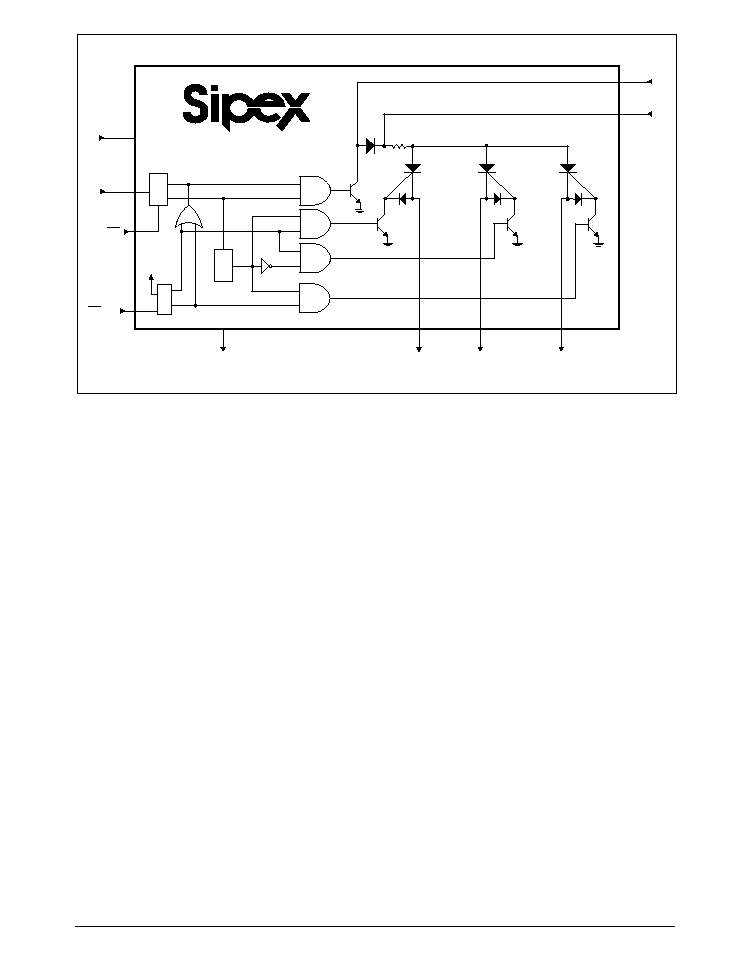
4
COIL
SP4490
f
COIL
f
LAMP1
f
LAMPCOM
SCR1
SCR2
EL1
V
SS
V
DD
SCR3
EL2
ELcommon
FF7
OSC
f
LAMP2
R
OSC
CAP
EL1/EL2
ON/OFF
V
DD
SEL
IN 0
1
6
7
7
8
10
5
1
4
2
3
DESCRIPTION
The SP4490 electroluminescent lamp driver pro-
vides designers of cell phones, PDA's and other
handheld, portable electronic devices with an
integrated solution for driving two EL lamps
independently. The SP4490 reduces system
cost, component count and board space require-
ments over a discrete 2 EL driver approach. The
EL lamp operates in opposite phase so the SP4490
can be easily implemented in applications driv-
ing multi-color or multi-segment EL lamps. The
SP4490 operates from a +2.2V to +6.0V battery
source. The device features a low power standby
mode that draws less than 1mA. The frequency
of the internal oscillator is set using a single
external resistor. A single external inductor is
required to generate the high voltage AC outputs
to drive the EL lamps. All input pins are ESD
protected with internal diodes to V
DD
and V
SS
.
The SP4490 contains a DC-AC inverter that can
produce an AC output of 180V
PP
(typical) from
a 3.0V input voltage. An internal block diagram
of the SP4490 can be found in Figure 1.
Electroluminescent Technology
An EL lamp consists of a thin layer of phospho-
rous material sandwiched between two strips of
plastic which emits light (flouresces) when a
high voltage AC signal is applied across it. It
behaves primarily as a capacitive load. Long
periods of DC voltage applied to the material
tend to reduce its lifetime. With these conditions
in mind, the ideal signal to drive an EL lamp is a
high voltage sine wave. Traditional approaches
to achieve this type of waveform include discrete
circuits incorporating a transformer, transistors
and several resistors and capacitors.
This approach is large and bulky and cannot be
implemented in most handheld equipment. Sipex
offers low power single chip driver circuits spe-
cifically designed to drive small to medium sized
electroluminescent panels. Sipex EL drivers
provide a differential AC voltage without a DC
offset to maximize EL lamp lifetime. The only
additional components required for the EL driver
circuitry are an inductor, resistor and capacitor.
Figure 1: Internal Block Diagram of SP4490
Rev. 9/12/00
SP4490 Two Panel Electroluminescent Lamp Driver
© Copyright 2000 Sipex Corporation
5
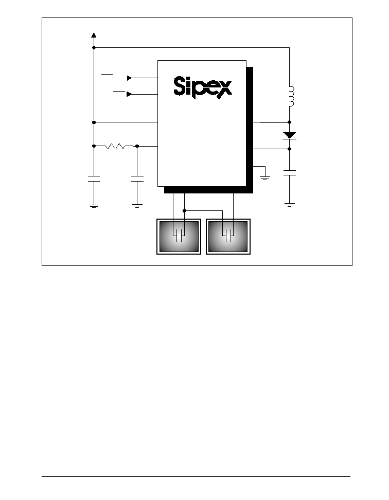
Figure 2: Typical Application Circuit of SP4490
R
OSC
V
SS
COIL
CAP
SP4490
V
BATT
C1
0.1
µ
F
R
OSC
464k
L1
470
µ
H
6
2
3
1
7
5
EL1/EL2
D1
1N4148
C
INT
1800pF
V
DD
ELcommon
EL1
EL Lamp
9
10
C2*
10nF
4
ON/OFF
* optional device
EL2
8
EL Lamp
Electroluminescent backlighting is ideal when
used with LCD displays, keypads or other back-
lit readouts. EL lamps uniformly light an area
without creating any undesirable "hot spots" in
the display. Also, an EL lamp typically con-
sumes less power that LED's or incandescent
bulbs in similar lighting situations. These fea-
tures make EL ideal for attractive, battery pow-
ered products.
THEORY OF OPERATION
Coil Switch
The SP4490 has an inductor-based boost con-
verter to generate the high voltage used to drive
the EL lamp. Energy is stored in the inductor
according to the equation E
L
= 1/2 (LI
pk
2
) where
I
pk
= (t
ON
) (V
BATT
- V
CEsat
) /L. An internal oscilla-
tor controls the coil switch. During the time the
coil switch is on, the coil is connected between
V
DD
and the saturation voltage of the
coil switch is on, the coil is connected between
V
DD
and coil switch and a magnetic field devel-
ops in the coil. When the coil switch turns off,
the switch opens, the magnetic field collapses
and the voltage across the coil rises. The internal
diode forward biases when the coil voltage rises
above the H-Bridge voltage and the energy en-
ters the EL lamp. Each pulse increases the
As the voltage approaches its maximum, the
steps become smaller. (see figure 4).
The brightness of the EL lamp output is directly
related to energy recovery in the boost converter.
There are many variations among coils such as
magnetic core differences, winding differences
and parasitic capacitances. For suggested coil
suppliers refer to page 10.
Oscillator
The internal oscillator generates a high frequency
clock used by the boost converter and H-