 | –≠–ª–µ–∫—Ç—Ä–æ–Ω–Ω—ã–π –∫–æ–º–ø–æ–Ω–µ–Ω—Ç: SP4491EU | –°–∫–∞—á–∞—Ç—å:  PDF PDF  ZIP ZIP |
Rev. 12/19/00
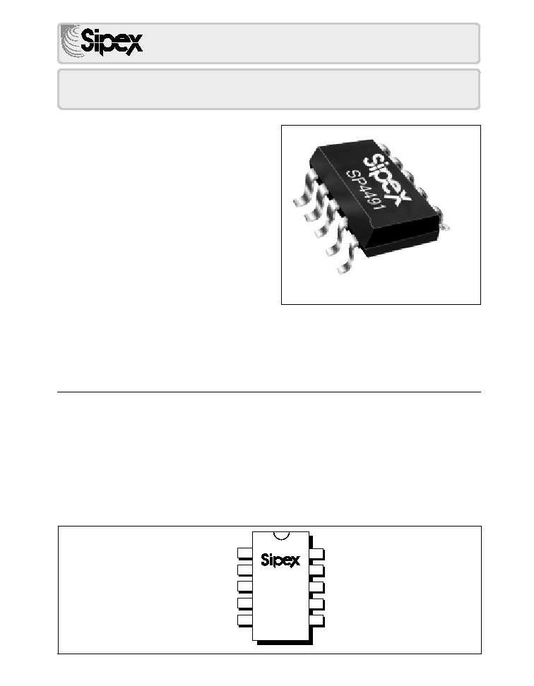
SP4491 Two Panel Electroluminescent Lamp Driver
© Copyright 2000 Sipex Corporation
1
s
Single IC Drives 2 EL Lamps
For Backlighting:
∑
Cell Phone Keypad & LCD
∑
Multi-Color EL Lamps
∑
Multi-Segment EL Lamps
s
Control Over Lamp-A & Lamp-B For
Independent Or Concurrent Operation
s
+2.2V to +6.0V Battery Operation
s
Single Coil Used To Generate High
Voltage AC Outputs
s
Low Power Standby Mode Draws 100nA
Typical Current
s
A Single Resistor Controls the Internal
Oscillator
s
DC-AC Inverter Produces Up To 220V
PP
s
Space-Saving 10MSOP Package
DESCRIPTION
The SP4491 electroluminescent lamp driver provides designers of cell phones PDA's and
other handheld, portable electronic devices with an integrated solution for driving two EL
lamps independently or concurrently. The SP4491 reduces system cost, component count
and board space requirements over a discrete 2-EL driver approach. The EL lamps operate
in opposite phase so the SP4491 can be easily implemented in applications driving multi-color
or multi-segment EL lamps. The SP4491 operates from a +2.2V to +6.0V battery source. The
device features a low power standby mode which draws less than 1
µ
A. The frequency of the
internal oscillator is set using a single external resistor. A single external inductor is required
to generate the high voltage AC outputs to drive the EL lamps. All input pins are ESD protected
with internal diodes to V
DD
and V
SS.
SP4491
Two Panel Electroluminscent Lamp Driver
APPLICATIONS
s
Cellular Phones
s
PDA's
s
Handheld GPS Units
s
Security Systems
s
POS Terminals
R
OSC
V
DD
ELcommon
EL1
1
2
3
4
7
8
9
10
V
SS
5
EL2
COIL
6
CAP
SP4491
ELEN1
ELEN2
Æ

Rev. 12/19/00
SP4490 Two Panel Electroluminescent Lamp Driver
© Copyright 2000 Sipex Corporation
2
ABSOLUTE MAXIMUM RATINGS
These are stress ratings only and functional operation of
the device at these ratings or any other above those
indicated in the operation sections of the specifications
below is not implied. Exposure to absolute maximum
rating conditions for extended periods of time may affect
reliability.
Power Supply, V
DD
.................................................7.0V
Input Voltages, Logic.....................-0.3V to (V
DD
+0.3V)
Lamp Outputs...................................................220V
P-P
Operating Temperature.........................-40∞C to +85∞C
Storage Temperature..........................-65∞C to +150∞C
Power Dissipation Per Package
10-pin MSOP
(derate 8.84mW/∞C above +70∞C)....................720mW
SPECIFICATIONS
V
DD
= +3.0V, LCOIL = 2.2mH, R
OSC
= 560k
, El Lamp Load = 4.7nF; CINT = 1000pF and T
AMB
= 25∞C unless otherwise noted.
STORAGE CONSIDERATIONS
Storage in a low humidity environment is pre-
ferred. Large high density plastic packages are
moisture sensitive and should be stored in Dry
Vapor Barrier Bags. Prior to usage, the parts
should remain bagged and stored below 40
∞
C and
60%RH. If the parts are removed from the bag,
they should be used within 48 hours or stored in an
environment at or below 20%RH. If the above
conditions cannot be followed, the parts should be
baked for four hours at 125
∞
C in order remove
moisture prior to soldering. Sipex ships product in
Dry Vapor Barrier Bags with a humidity indicator
card and desiccant pack. The humidity indicator
should be below 30%RH.
The information furnished by Sipex has been care-
fully reviewed for accuracy and reliability. Its applica-
tion or use, however, is solely the responsibility of the
user. No responsibility for the use of this information
become part of the terms and conditions of any
subsequent sales agreement with Sipex. Specifica-
tions are subject to change without no responsibility
for any infringement of patents or other rights of third
parties which may result from its use. No license or
other proprietary rights are granted by implication or
otherwise under any patent or patent rights of Sipex
Corporation.
R
E
T
E
M
A
R
A
P
.
N
I
M
.
P
Y
T
.
X
A
M
S
T
I
N
U
S
N
O
I
T
I
D
N
O
C
V
,
e
g
a
t
l
o
V
y
l
p
p
u
S
D
D
2
.
2
6
V
I
,
t
n
e
r
r
u
C
y
l
p
p
u
S
D
D
0
1
4
5
A
m
V
,
e
g
a
t
l
o
V
li
o
C
L
I
O
C
V
D
D
9
V
V
,
e
g
a
t
l
o
V
t
u
p
n
I
2
N
E
L
E
/
1
N
E
L
E
N
E
L
E
W
O
L
H
G
I
H
5
2
.
0
-
V
D
D
5
2
.
0
-
0
V
D
D
V
5
2
.
0
V
D
D
5
2
.
0
+
V
I
,
t
n
e
r
r
u
C
n
w
o
d
t
u
h
S
D
S
I
=
L
I
O
C
I
+
D
D
1
.
1
µ
A
V
N
E
L
E
V
0
=
E
V
I
R
D
R
O
T
C
U
D
N
I
f
,
y
c
n
e
u
q
e
r
F
li
o
C
L
I
O
C
0
.
6
3
0
.
2
3
0
.
4
4
7
.
5
5
2
.
8
5
z
H
k
T
B
M
A
5
2
+
=
O
C
T
B
M
A
0
4
-
=
O
5
8
+
o
t
C
O
C
e
l
c
y
C
y
t
u
D
li
o
C
0
9
%
T
B
M
A
5
2
+
=
O
C
I
,
t
n
e
r
r
u
C
li
o
C
L
I
O
C
9
5
4
A
m
I
,
t
n
e
r
r
u
C
li
o
C
k
a
e
P
L
I
O
C
-
K
P
0
2
0
9
A
m
T
U
P
T
U
O
P
M
A
L
L
E
f
,
y
c
n
e
u
q
e
r
F
p
m
a
L
L
E
P
M
A
L
1
8
2
0
5
2
3
4
3
5
3
4
5
5
4
z
H
T
B
M
A
5
2
+
=
O
V
,
C
D
D
V
0
.
3
+
=
T
B
M
A
0
4
-
=
O
5
8
+
o
t
C
O
C
V
,
e
g
a
t
l
o
V
t
u
p
t
u
O
k
a
e
P
o
t
k
a
e
P
K
P
-
K
P
0
4
1
2
0
2
V
T
B
M
A
5
2
+
=
O
C
Rev. 12/19/00
SP4491 Two Panel Electroluminescent Lamp Driver
© Copyright 2000 Sipex Corporation
3
PIN ASSIGNMENTS
Pin 1 -- ELEN1 -- Electroluminescent Lamp
Enable Control Line 1. This is a control line
to enable a single or dual EL lamp output.
Refer to Table 1 for the control logic.
Pin 2 -- V
DD
-- Positive Battery Power Supply.
Connect such that +2.636V < V
DD
< +3.15V.
Pin 3 -- R
OSC
-- Oscillator Resistor. Connecting
a resistor between this input pin andV
DD
sets
the frequency of the internal clock.
Pin 4 -- ELEN2 -- Electroluminescent Lamp
Enable Control Line 2. This a control line to
enable a single or dual EL lamp output. Refer
to Table 1 for the control logic.
Pin 5 -- V
SS
-- Power Supply Common. Con-
nect to the lowest circuit potential, typically
ground.
Pin 6 -- COIL -- Coil. The inductor for the
boost converter is connected from V
BATT
to
this input pin.
Pin 7 -- CAP -- Integrator Capacitor. An
integrating capacitor (1800pF typically)
connected from this pin to ground filters out
any coil switching spikes or ripple present in
the output waveform to the EL lamps. Con-
necting a fast recovery diode from COIL to
CAP increases the light output of the EL
lamp.
Pin 8 -- EL COMMON -- Electroluminescent
Common. This is a high voltage lamp driver
output pin common to both EL lamps.
Pin 9 -- EL2 -- Electroluminescent Lamp Out-
put 2. This is a high voltage lamp driver
output pin connect to the second EL lamp.
Pin 10 -- EL1 -- Electroluminescent Lamp
Output 1. This is a high voltage lamp driver
output pin to connect to the first EL lamp.
PINOUT
R
OSC
V
DD
ELcommon
EL1
1
2
3
4
7
8
9
10
V
SS
5
EL2
COIL
6
CAP
SP4491
ELEN1
ELEN2
Rev. 12/19/00
SP4490 Two Panel Electroluminescent Lamp Driver
© Copyright 2000 Sipex Corporation
4
Figure 1: Internal Block Diagram of SP4491
1
N
E
L
E
2
N
E
L
E
t
u
p
t
u
O
1
L
E
t
u
p
t
u
O
2
L
E
0
0
F
F
O
F
F
O
0
1
F
F
O
N
O
1
0
N
O
F
F
O
1
1
N
O
N
O
Table 1: Control Line Logic Table
COIL
SP4491
f
COIL
f
LAMP1
f
LAMPCOM
EL Lamp
SCR1
SCR2
EL1
V
SS
V
DD
V
BATT
L1
2.2mH
EL Lamp
SCR3
EL2
ELcommon
C
INT
1000pF
D1
1N4148
FF7
OSC
f
LAMP2
R
OSC
V
BATT
560k
CAP
C2*
1nF
C1
0.1
µ
F
* optional device
ELEN2
0
1
6
9
9
8
10
5
4
2
3
ELEN1
1
Rev. 12/19/00
SP4491 Two Panel Electroluminescent Lamp Driver
© Copyright 2000 Sipex Corporation
5
DESCRIPTION
The SP4491 electroluminescent lamp driver pro-
vides designers of cell phones, PDA's and other
handheld, portable electronic devices with an
integrated solution for driving two EL lamps
independently or stimultaneously. The SP4491
reduces system cost, component count and board
space requirements over a discrete 2 EL driver
approach. The EL lamps operate in opposite
phase so the SP4491 can be easily implemented
in applications driving multi-color or multi-seg-
ment EL lamps. The SP4491 operates from a
+2.2V to +6.0V battery source. The device
features a low power standby mode that draws
less than 1
µ
A. The frequency of the internal
oscillator is set using a single external resistor. A
single external inductor is required to generate
the high voltage AC outputs to drive the EL
lamps. All input pins are ESD protected with
internal diodes to V
DD
and V
SS
.
The SP4491 contains a DC-AC inverter that can
produce an AC output of 180V
PP
(typical) from
a 3.0V input voltage. An internal block diagram
of the SP4491 can be found in Figure 1.
Electroluminescent Technology
An EL lamp consists of a thin layer of phospho-
rous material sandwiched between two strips of
plastic which emits light (flouresces) when a
high voltage AC signal is applied across it. It
behaves primarily as a capacitive load. Long
periods of DC voltage applied to the material
tend to reduce its lifetime. With these conditions
in mind, the ideal signal to drive an EL lamp is a
high voltage sine wave. Traditional approaches
to achieve this type of waveform include discrete
circuits incorporating a transformer, transistors
and several resistors and capacitors.
This approach is large and bulky and cannot be
implemented in most handheld equipment. Sipex
offers low power single chip driver circuits spe-
cifically designed to drive small to medium sized
electroluminescent panels. Sipex EL drivers
provide a differential AC voltage without a DC
offset to maximize EL lamp lifetime. The only
additional components required for the EL driver
circuitry are an inductor, resistor and capacitor.
Figure 2: Typical Application Circuit of SP4491
R
OSC
V
SS
COIL
CAP
SP4491
V
BATT
C1
0.1
µ
F
R
OSC
464k
L1
470
µ
H
6
2
3
1
7
5
ELEN1
D1
1N4148
C
INT
1800pF
V
DD
ELcommon
EL1
EL Lamp
9
10
C2*
1nF
4
ELEN2
* optional device
EL2
8
EL Lamp

Rev. 12/19/00
SP4490 Two Panel Electroluminescent Lamp Driver
© Copyright 2000 Sipex Corporation
6
An external resistor from VDD to ROSC sets the
oscillator frequency. Typically a 560k
resistor
sets the frequency to 44.0kHz. The high fre-
quency clock directly controls the coil switch.
This high frequency clock is divided by 128 to
generate a low frequency clock which controls
the EL H-Bridge and sets the EL lamp fre-
quency. The oscillator has low sensitivity to
temperature and supply voltage variations, in-
creasing the performance of the EL driver over
the operating parameters.
Dual H-Bridge
The H-Bridge consists of two SCR structures
and two NPN transistors that control how the
lamp is charged. Setting ON/OFF to HIGH
activates the H-Bridge that is selected by EL1/
EL2. If the EL1/EL2 is low, EL1 is illuminated.
If EL1/EL2 is HIGH, EL2 is illuminated. The
EL driver illuminates the lamp by applying the
high voltage supply of the boost converter to the
lamp terminals through the H-Bridge and then
switching the terminal polarity between the high
voltage supply and ground at a constant fre-
quency. This applies an AC voltage to the lamp
that is twice the peak output voltage of the boost
driver. An AC voltage greater than the 40V
across the terminals of the lamp is typically
necessary to adequately illuminate the EL lamp.
Setting ON/OFF to LOW disables the outputs
and places the circuit in a low power state.
DESIGN CONSIDERATIONS
Inductor Selection
If limiting peak current draw from the power
supply is important, small coil values (<1mH)
may need a higher oscillator frequency. Inductor
current ramps faster in a lower inductance coil
than a higher inductance coil for a given coil
switch on time period, resulting in higher peak
coil currents.
It is important to observe the saturation current
rating of a coil. When this current is exceeded,
the coil is incapable of storing any more energy
and then ceases to act as an inductor. Instead, the
coil behaves according to its series DC resis-
tance.
Electroluminescent backlighting is ideal when
used with LCD displays, keypads or other back-
lit readouts. EL lamps uniformly light an area
without creating any undesirable "hot spots" in
the display. Also, an EL lamp typically con-
sumes less power that LED's or incandescent
bulbs in similar lighting situations. These fea-
tures make EL ideal for attractive, battery pow-
ered products.
THEORY OF OPERATION
Coil Switch
The SP4491 has an inductor-based boost con-
verter to generate the high voltage used to drive
the EL lamp. Energy is stored in the inductor
according to the equation E
L
= 1/2 (LI
pk
2
) where
I
pk
= (t
ON
) (V
BATT
- V
CEsat
) /L. An internal oscilla-
tor controls the coil switch. During the time the
coil switch is on, the coil is connected between
V
DD
and the saturation voltage of the coil switch.
While the coil is connected between V
DD
and coil
switch and a magnetic field develops in the coil.
When the coil switch turns off, the switch opens,
the magnetic field collapses and the voltage
across the coil rises. The internal diode forward
biases when the coil voltage rises above the H-
Bridge voltage and the energy enters the EL
lamp. Each pulse increases the voltage across
the lamp in discrete steps.
As the voltage approaches its maximum, the
steps become smaller. (see figure 4).
The brightness of the EL lamp output is directly
related to energy recovery in the boost converter.
There are many variations among coils such as
magnetic core differences, winding differences
and parasitic capacitances. For suggested coil
suppliers refer to page 10.
Oscillator
The internal oscillator generates a high frequency
clock used by the boost converter and H-Bridge.
And

Rev. 12/19/00
SP4491 Two Panel Electroluminescent Lamp Driver
© Copyright 2000 Sipex Corporation
7
Since small coils (<1mH) have inherently low
series DC resistance, the current can peak dra-
matically through a small coil during saturation.
This situation results in wasted energy not stored
in the magnetics of the coil but expressed as
heating which could lead to failure of the coil.
Generally, selecting a coil with lower series DC
resistance will result in a system with higher
efficiency and lamp brightness.
Lamp Effects
EL lamp parameters vary between manufactur-
ers. Series DC resistance, lighting efficiency
and lamp capacitance per area differ the most
overall. Larger lamps require more energy to
illuminate. Lowering the oscillator frequency
allows more energy to be stored in the coil during
each coil switch cycle and increases lamp bright-
ness. The oscillator frequency can be lowered to
a point where the lamp brightness then begins to
drop because the lamp frequency must be above
a critical frequency (approx. 100Hz) to light.
Lamp color is affected by the switching fre-
quency of the EL driver. Green EL lamps will
emit a more blue light as EL lamp frequency
increases.
Noise Decoupling on Logic Inputs
If EL1/EL2 or ON/OFF are connected to traces
susceptible to noise, it may be necessary to
connect bypass capacitor of approximately 10nF
between EL1/EL2 and VSS, and ON/OFF and
VSS. If these inputs are driven by a micropro-
cessor which provides a low impedance HIGH
and LOW signal, then noise bypassing may not
ber be necessary.
Increasing Light Output
EL lamp light output can be improved by con-
necting a fast recovery diode from the COIL pin
to the CAP pin. The internal diode is bypassed
resulting in an increase in light output at the EL
lamp. We suggest a fast recovery diode such as
the industry standard 1N4148.
The optimal value of C
INT
will vary depending on
the lamp parameters and coil value. Lower C
INT
values can decrease average supply current but
higher C
INT
values can increase lamp brightness.
This is best determined by experimentation. A
rule of thumb is larger coils (1mH) are paired
with a smaller C
INT
(680pF) and smaller coils
(470
µ
H) are paired with a larger C
INT
(1800pF).
Changing the EL lamp Output Voltage
Waveform
Designers can alter the sawtooth output voltage
waveform to the EL lamp. Increasing the capaci-
tance of the integration capacitor, C
INT,
will inte-
grate the sawtooth waveform making it appear
more like a square wave.
Printed Circuit Board Layout Sugges-
tions
The EL driver's high-frequency operation makes
PCB layout important for minimizing electrical
noise. Keep the IC's GND pin and the ground
leads of C1 and C
INT
less than 0.2in (5mm) apart.
Also keep the connections to the COIL pin as
short as possible. To maximize output power
and efficiency and minimize output ripple volt-
age, use a ground plane and solder the IC's VSS
pin directly to the ground plane.
EL Lamp Driver Design Challenges
There are many
variables which can be opti-
mized for specific applications. The amount of
light emitted is a function of the voltage applied
to the lamp, the frequency at which is applied, the
lamp material, the lamp size, and the inductor
used. Sipex supplies characterization charts to
aid the designer in selecting the optimum circuit
configuration.
Sipex will perform customer application evalu-
ations, using the customer's actual EL lamp to
determine the optimum operating conditions for
specific applications. For customers consider-
ing an EL backlighting solution for the first time,
Sipex is able to provide retrofits to non-backlit
products for a thorough electrical and cosmetic
evaluation. Please contact your local Sipex sales
Representative or the Sipex factory directly to
initiate this valuable service.
Rev. 12/19/00
SP4490 Two Panel Electroluminescent Lamp Driver
© Copyright 2000 Sipex Corporation
8
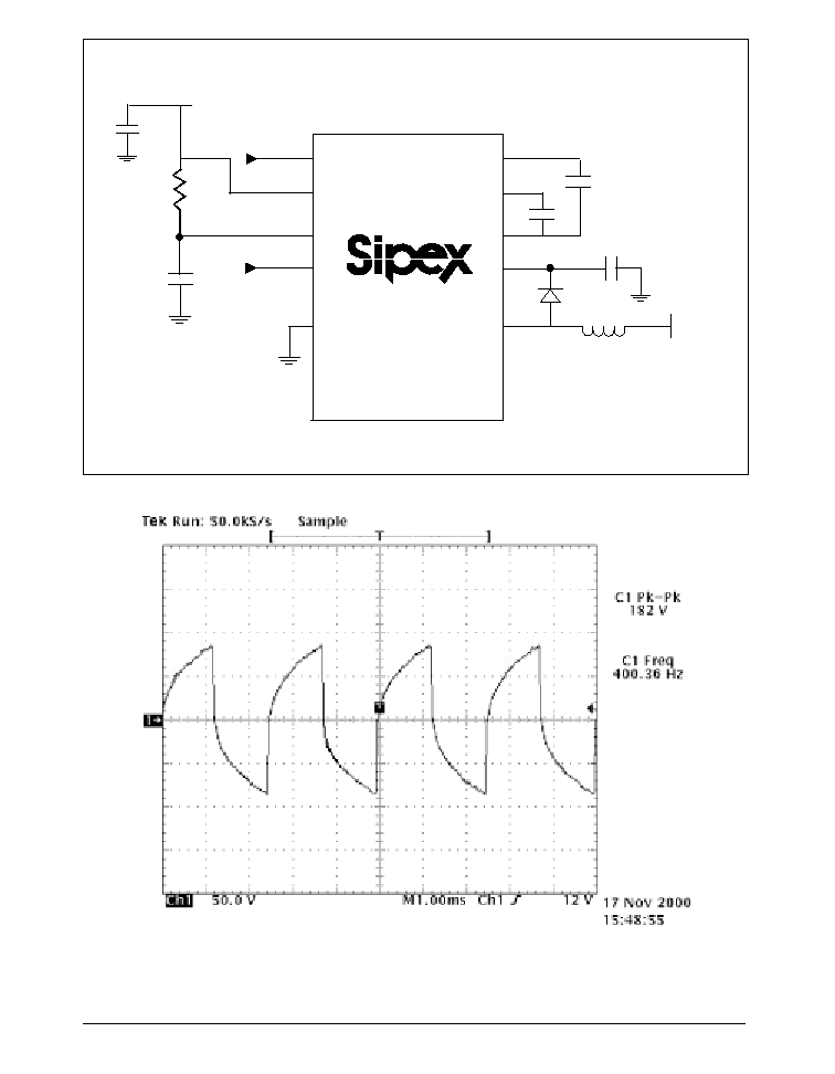
Figure 3: Test Circuit Diagram of SP4491
R
OSC
SP4491
3
4
2
7
6
EL1
1N4148
1
EL Common
EL2
EL2
5
V
SS
10
9
8
EL1
COIL
CAP
+3V
1000pF
C
EL1
+3V
2.2mh 28 ohm
10nF
560K
V
DD
C
EL2
4.7nf
4.7nf
0.1uF
Figure 4: Typical EL Lamp Voltage Waveform
Rev. 12/19/00
SP4491 Two Panel Electroluminescent Lamp Driver
© Copyright 2000 Sipex Corporation
9
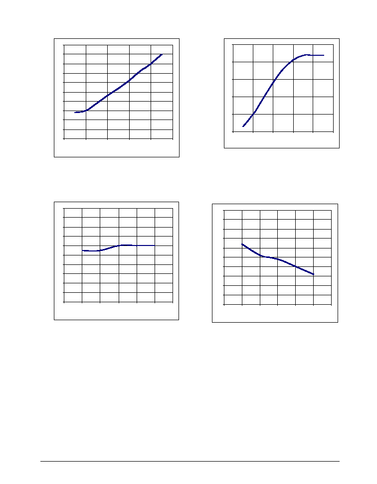
PERFORMANCE CHARACTERISTICS
Figure 5
0
5
10
15
20
25
30
35
40
45
50
50
150
250
350
450
550
Resistance (kOhm)
0
5
10
15
20
25
50
150
250
350
450
550
Resistance (kOhm)
20
22
24
26
28
30
32
34
36
38
40
0.5
1
1.5
2
2.5
3
3.5
Lamp Size (in
2
)
140
150
160
170
180
190
200
210
220
230
240
0.5
1
1.5
2
2.5
3
3.5
Lamp Size (in
2
)
Supply Current vs Rosc
Vdd = 3V, L = 470uH
Supply Current (mA)
Luminance vs Rosc
Vdd = 3V, L = 470uH
Luminance (cd/m
2
)
Figure 7
Frequency (kHz)
Lamp Frequency vs. Rosc
Vdd = 3V, L = 470uH
Output Voltage vs. Rosc
Vdd = 3V, L = 470uH
Figure 8
Figure 6
Output Voltage (V)
Rev. 12/19/00
SP4490 Two Panel Electroluminescent Lamp Driver
© Copyright 2000 Sipex Corporation
10
0
5
10
15
20
25
30
35
0.5
1
1.5
2
2.5
3
3.5
Lamp Size (in
2
)
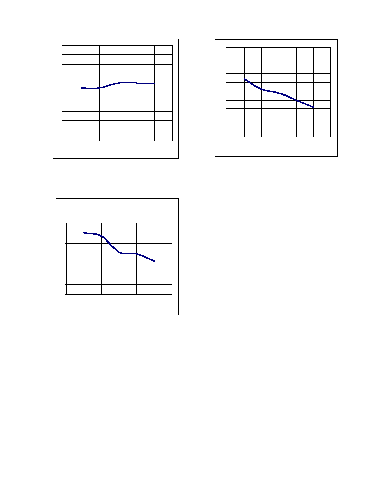
PERFORMANCE CHARACTERISTICS
Figure 9
Supply Current vs. Lamp Size
Supply Current (mA)
Luminance vs. Lamp Size
Vdd = 3V, L = 470uH
Luminance (cd/m
2
)
Figure 10
20
22
24
26
28
30
32
34
36
38
40
0.5
1
1.5
2
2.5
3
3.5
Lamp Size (in
2
)
140
150
160
170
180
190
200
210
220
230
240
0.5
1
1.5
2
2.5
3
3.5
Lamp Size (in
2
)
Vdd = 3V, L = 470uH
Figure 11
Vdd = 3V, L = 470uH
Output Voltage vs. Lamp Size
Output Voltage (Vp-p)

Rev. 12/19/00
SP4491 Two Panel Electroluminescent Lamp Driver
© Copyright 2000 Sipex Corporation
11
EL Lamp Manufacturers
Leading Edge Ind. Inc.
11578 Encore Circle
Minnetonka, MN 55343
Phone 1-800-845-6992
Midori Mark Ltd.
1-5 Komagata 2-Chome
Taita-Ku 111-0043 Japan
Phone: 81-03-3848-2011
Luminescent Systems inc. (LSI)
101 Etna Road
Lebanon, NH. 03766-9004
Phone: (603) 448-3444
Fax: (603) 448-3452
Polarizers/transflector Mnfg.
Nitto Denko
Yoshi Shinozuka
Bayside Business Park 48500
Fremont, CA. 94538
Phone: 510 445 5400
Fax: 510 445-5480
Top Polarizer- NPF F1205DU
Bottom - NPF F4225
or (F4205) P3 w/transflector
Transflector Material
Astra Products
Mark Bogin
P.O. Box 479
Baldwin, NJ 11510
Phone (516)-223-7500
Fax (516)-868-2371
NEC Corporation
Yumi Saskai
7-1, Shiba 5 Chome, Minato-ku,
Tokyo 108-01, Japan
Phone: (03) 3798-9572
Fax: (03) 3798-6134
Seiko Precision
Shuzo Abe
1-1, Taihei 4-Chome,
Sumida-ku, Tokyo, 139 Japan
Phone: (03) 5610-7089
Fax: (03) 5610-7177
Gunze Electronics
2113 Wells Branch Parkway
Austin, TX 78728
Phone: (512) 752-1299
Fax: (512) 252-1181
Coil Manufacturers
Hitachi Metals
Material Trading Division
2101 S. Arlington Heights Road,
Suite 116
Arlington Heights, IL 60005-4142
Phone: 1-800-777-8343 Ext. 12
(847) 364-7200 Ext. 12
Fax: (847) 364-7279
Hitachi Metals Ltd. Europe
Immernannstrasse 14-16, 40210
Dusseldorf, Germany
Contact: Gary Loos
Phone: 49-211-16009-0
Fax: 49-211-16009-29
Hitachi Metals Ltd.
Kishimoto Bldg. 2-1, Marunouchi
2-chome, Chiyoda-Ku, Tokyo, Japan
Contact: Mr. Noboru Abe
Phone: 3-3284-4936
Fax: 3-3287-1945
Hitachi Metals Ltd. Singapore
78 Shenton Way #12-01,
Singapore 079120
Contact: Mr. Stan Kaiko
Phone: 222-8077
Fax: 222-5232
Hitachi Metals Ltd. Hong Kong
Room 1107, 11/F., West Wing,
Tsim Sha. Tsui Center 66
Mody Road,Tsimshatsui East,
Kowloon, Hong Kong
Phone: 2724-4188
Fax: 2311-2095
Panasonic.
6550 Katella Ave
Cypress, CA 90630-5102
Phone: (714) 373-7366
Fax: (714) 373-7323
Sumida Electric Co., LTD.
5999, New Wilke Road,
Suite #110
Rolling Meadows, IL,60008 U.S.A.
Phone: (847) 956-0666
Fax: (847) 956-0702
Sumida Electric Co., LTD.
4-8, Kanamachi 2-Chrome,
Katsushika-ku, Tokyo 125 Japan
Phone: 03-3607-5111
Fax: 03-3607-5144
Sumida Electric Co., LTD.
Block 15, 996, Bendemeer Road
#04-05 to 06, Singapore 339944
Republic of Singapore
Phone: 2963388
Fax: 2963390
Sumida Electric Co., LTD.
14 Floor, Eastern Center, 1065
King's Road, Quarry Bay,
Hong Kong
Phone: 28806688
Fax: 25659600
Murata
2200 Lake Park Drive, Smyrna
Georgia 30080 U.S.A.
Phone: (770) 436-1300
Fax: (770) 436-3030
Murata European
Holbeinstrasse 21-23, 90441
Numberg, Postfachanschrift 90015
Phone: 011-4991166870
Fax: 011-49116687225
Murata Taiwan Electronics
225 Chung-Chin Road, Taichung,
Taiwan, R.O.C.
Phone: 011 88642914151
Fax: 011 88644252929
Murata Electronics Singapore
200 Yishun Ave. 7, Singapore
2776, Republic of Singapore
Phone: 011 657584233
Fax: 011 657536181
Murata Hong Kong
Room 709-712 Miramar Tower, 1
Kimberly Road, Tsimshatsui,
Kowloon, Hong Kong
Phone: 011-85223763898
Fax: 011-85223755655
Rev. 12/19/00
SP4490 Two Panel Electroluminescent Lamp Driver
© Copyright 2000 Sipex Corporation
12
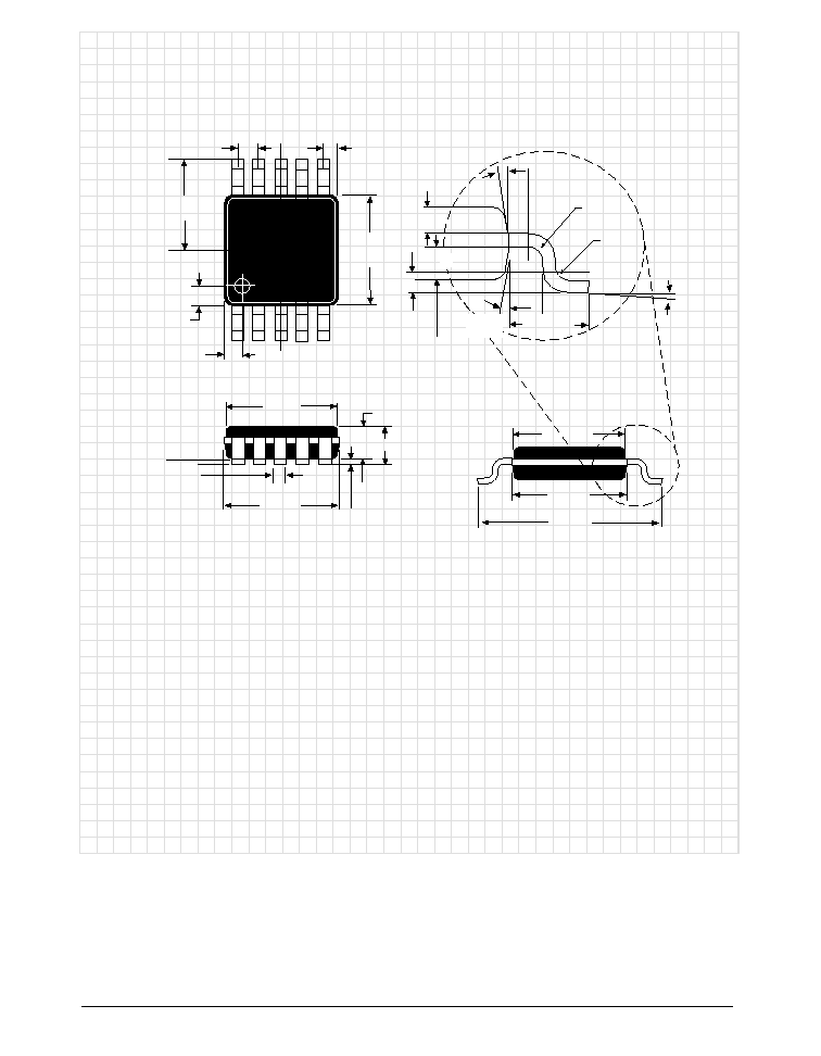
PACKAGE: 10-PIN MSOP PACKAGE
(ALL DIMENSIONS IN MILLIMETERS)
1
0.50
BSC
3.00
±
0.10
2
2.95
±
0.10
0.86
±
0.08
1.10 MAX
0.10
±
0.05
3.00
±
0.10
3.00
±
0.10
0.95BSC
0.55
±
0.15
0.30 to 0.07
0.41
±
0.08
2.95
±
0.10
3.0
o
±
3.0
o
2.95
±
0.10
0.51
±
0.13
0.51
±
0.13
0.25
0.31
±
0.08
4.90
±
0.15
0.50
BSC
12.0
o
±
3.0
o
12.0
o
±
3.0
o
0.30 to 0.07
0.23
±
0.07
Rev. 12/19/00
SP4491 Two Panel Electroluminescent Lamp Driver
© Copyright 2000 Sipex Corporation
13
ORDERING INFORMATION
Model
Temperature Range
Package Type
SP4491EU .............................................. -40∞C to +85∞C ........................................ 10-Pin MSOP
SP4491UEB ........................................................................................................ Evaluation Board
Sipex Corporation reserves the right to make changes to any products described herein. Sipex does not assume any liability arising out of the
application or use of any product or circuit described hereing; neither does it convey any license under its patent rights nor the rights of others.
Corporation
SIGNAL PROCESSING EXCELLENCE
Sipex Corporation
Headquarters and
Sales Office
22 Linnell Circle
Billerica, MA 01821
TEL: (978) 667-8700
FAX: (978) 670-9001
e-mail: sales@sipex.com
Sales Office
233 South Hillview Drive
Milpitas, CA 95035
TEL: (408) 934-7500
FAX: (408) 935-7600