Rev. 7/2/03
SP6121 Low Voltage, 8 Pin, Synchronous Buck Controller © Copyright 2003 Sipex Corporation
1
SP6121
Optimized for Single Input Voltage - 3V to 5.5V
High Efficiency: Greater than 95% possible
Accurate, 500kHz Fixed Frequency Operation
Fast Transient Response
500
µ
A, I
Q
(25
µ
A in Shutdown)
Internal, 0.4 V/ms, Soft Start Circuit
Precision 1% Reference
Resistor Programmable Output Voltage
Lossless Adjustable Current Limit with
High Side R
DS(ON)
Sensing
0% to 100% Duty Cycle Range
High Side PMOS Switch Negates Need for
External Charge Pump
Output Over Voltage Protection
Hiccup Mode Current Limit Protection
Low Voltage, 8 Pin, Synchronous Buck Controller
Ideal for 2A to 10A, Small Footprint, DC-DC Power Converters
APPLICATIONS
Supply Bias for
- DSP
- Microprocessor Core
- I/O & Logic
Video Cards
Board Level Supply in
Distributed Power Systems
Æ
DESCRIPTION
The SP6121 is a fixed frequency, voltage mode, synchronous PWM controller designed to work
from a single 5V or 3.3V input supply, providing excellent AC and DC regulation for high efficiency
power conversion. The operating frequency is internally set at 500kHz, permitting the use of
small, surface mount inductors and capacitors. Requiring only few external components, the
SP6121 packaged in an 8-pin SOIC, is especially suited for low voltage applications where cost,
small size and high efficiency are critical. With its low voltage capability and inherent 100% duty
cycle operation, the SP6121 allows low dropout operation in the event of a low input supply
voltage condition.
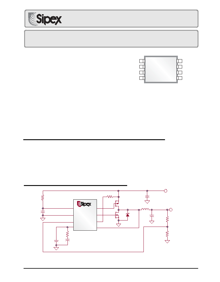
Q1 = FAIRCHILD FDS6375
Q2 = FAIRCHILD FDS6690A
DS = STMICROELECTRONICS STPS2L25BU
L1 = PANASONIC ETQ-P6F1R6SFA
C
OUT
= SANYO 4TPB470M
1
2
3
4
5
6
7
8
COMP
V
FB
GND
PDRV
NDRV
I
SET
I
SENSE
V
CC
SP6121
8 Pin SOIC
V
CC
CB
3.3
µ
F
C
IN
47
µ
F
Ceramic 6.3V
I
SET
3.3V
V
IN
PDRV
GND
COMP
SP6121
U1
Æ
Æ
V
FB
NDRV
I
SENSE
CP
50pF
RZ
10k
V
OUT
1.8
µ
H
L1
C
OUT
470
µ
F x 2
RSET
2.3k
1.9V 8A
Q1
CZ
3.7nF
Q2
RV
CC
5
DS
R1
5.2k
R2
10k
FEATURES
TYPICAL APPLICATION CIRCUIT

Rev. 7/2/03
SP6121 Low Voltage, 8 Pin, Synchronous Buck Controller © Copyright 2003 Sipex Corporation
2
PARAMETER
MIN
TYP
MAX
UNITS CONDITIONS
QUIESCENT CURRENT
V
CC
Supply Current
-
0.5
1.0
mA
No Switching
V
CC
Supply Current (Disabled)
-
25
60
µ
A
COMP = 0V
ERROR AMPLIFIER
Error Amplifier Transconductance
600
µ
s
COMP Sink Current
15
35
65
µ
A
V
FB
= 1.35V, COMP=0.8V, No Faults
COMP Source Current
15
35
65
µ
A
V
FB
=1.15V, COMP=1.8V
COMP Output Impedance
3
M
V
FB
Input Bias Current
100
nA
ERROR AMPLIFIER REFERENCE
Initial Accuracy
1.238
1.250
1.262
V
Trimmed with Error Amp in Unity Gain
Error Amplifier Reference over
1.225
1.250
1.275
V
Line, Load and Temperature
OSCILLATOR & DELAY PATH
Internal Oscillator Frequency
440
500
560
kHz
Maximum Duty Cycle
100
-
-
%
COMP = 2V
Minimum Duty Cycle
-
-
0
%
COMP = 0.8V
Minimum PDRV Pulse Width
100
ns
V
CC
> 4.5V, Ramp up COMP voltage
until PDRV starts switching
CURRENT LIMIT
Internal Current Limit Threshold
125
160
195
mV
V
ISET
- V
ISENSE
, T
A
= 25
∞
C
ISET Sink Current
25
30
35
µ
A
V
ISET
=5V, T
A
= 25
∞
C
Current Limit Threshold and
0.33
%/C
ISET Temperature Coefficient
Current Limit Time Constant
15
µ
s
ISENSE Input Bias Current
-
-
100
nA
SOFT START, SHUTDOWN, UVLO
Internal Soft Start Slew Rate
0.4
V/ms
Measured at COMP pin on the
transition from shutdown
Internal Soft Start Delay Time
1.5
ms
COMP charging to PDRV switching
COMP Discharge Current
150
300
µ
A
COMP = 0.5V, Fault Initiated
COMP Clamp Voltage
0.6
0.7
0.8
V
V
FB
= 1.3V
COMP Clamp Current
100
µ
A
COMP = 0.5V, V
FB
=1.15V
ELECTRICAL SPECIFICATIONS
Unless otherwise specified: 0
∞
C < T
A
< 70
∞
C, 3.0V < V
CC
< 5.5V, C
COMP
= 22nF, C
PDRV
= C
NDRV
= 3.3nF, V
FB
= 1.25V, I
SET
= I
SENSE
= V
CC
, GND=0V
These are stress ratings only and functional
operation of the device at these ratings or any other
above those indicated in the operation sections of
the specifications below is not implied. Exposure to
absolute maximum rating conditions for extended
periods of time may affect reliability.
V
CC ......................................................................................................
7V
All other pins ............................... -0.3V to V
CC
+0.3V
Peak Output Current < 10
µ
s
PDRV, NDRV ....................................................... 2A
Storage Temperature ...................... -65
∞
C to 150
∞
C
Lead Temperature (Soldering, 10 sec) .......... 300
∞
C
ESD Rating ............................................... 2kV HBM
ABSOLUTE MAXIMUM RATINGS
Rev. 7/2/03
SP6121 Low Voltage, 8 Pin, Synchronous Buck Controller © Copyright 2003 Sipex Corporation
3
PIN DESCRIPTION
PIN NO.
PIN NAME DESCRIPTION
1
V
CC
Positive input supply for the control circuitry and gate drivers. Properly bypass this pin
to GND with a low ESL/ESR ceramic capacitor.
2
GND
Ground pin. Both power and control circuitry of the IC is referenced to this pin.
3
V
FB
Feedback Voltage Pin. It is the inverting input of the Error Amplifier and serves as the
output voltage feedback point for the buck converter. The output voltage is sensed and
can be adjusted through an external resistor divider.
4
COMP
Output of the Error Amplifier. It is internally connected to the non-inverting input of the
PWM comparator. A lead-lag network is typically connected to the COMP pin to
compensate the feedback loop in order to optimize the dynamic performance of the
voltage mode control loop. Sleep mode can be invoked by pulling the COMP pin below
0.2V with an external open-drain or open-collector transistor. Supply current is reduced
to 25
µ
A (typical) in shutdown. An internal 5
µ
A pull-up ensures start-up.
5
I
SENSE
Current Limit Sense pin. Connect this pin to the switching node at the junction between
the two external power MOSFET transistors. This pin monitors the voltage dropped
across the R
DS(ON)
of the high side P-channel MOSFET while it is conducting. When
this drop exceeds the sum of the voltage programmed through the I
SET
pin plus the
internal 160mV threshold, the overcurrent comparator sets the fault latch and termi-
nates the output pulses. The controller stops switching and goes through a hiccup
sequence. This prevents excessive power dissipation in the external power MOSFETs
during an overload condition. An internal delay circuit prevents that very short and mild
overload conditions, that could occur during a load transient, activate the current limit
circuit.
6
I
SET
Current Limit Threshold pin. An external resistor connected between this pin and the
source of the high side P-channel MOSFET adds to the internal current limit threshold
of 160mV. If a current limit threshold in excess of 160mV is required, the external
programming resistor can properly be chosen based on the internal 30
µ
A pull down
current available on the I
SET
pin. Both this 30
µ
A current source and the 160mV built-in
current limit threshold have a positive temperature coefficient to provide first order
correction for the temperature coefficient of the external P-channel MOSFET's R
DS(ON)
.
7
NDRV
High current driver output for the low side MOSFET switch. It is always low if PDRV is
low or during a fault.
8
PDRV
High current driver output for the high side MOSFET switch. It is always high if NDRV
is high or during a fault.
ELECTRICAL SPECIFICATIONS: Continued
Unless otherwise specified: 0
∞
C < T
A
< 70
∞
C, 3.0V < V
CC
< 5.5V, C
COMP
= 22nF, C
PDRV
= C
NDRV
= 3.3nF, V
FB
= 1.25V, I
SET
= I
SENSE
= V
CC
, GND=0V
PARAMETER
MIN
TYP
MAX
UNITS CONDITIONS
SOFT START, SHUTDOWN, UVLO: continued
Shutdown Threshold Voltage
0.2
0.3
0.4
V
Measured at COMP Pin
Shutdown Input Pull-up Current
5
µ
A
COMP = 0.2V, Measured at COMP pin
V
CC
Start Threshold
2.69
2.79
2.89
V
V
CC
Stop Threshold
2.59
2.69
2.79
V
V
CC
Hysteresis
-
100
-
mV
GATE DRIVERS
PDRV Rise Time
-
40
110
ns
V
CC
> 4.5V
PDRV Fall Time
-
40
110
ns
V
CC
> 4.5V
NDRV Rise Time
-
40
110
ns
V
CC
> 4.5V
PDRV Fall Time
-
40
110
ns
V
CC
> 4.5V
PDRV to NDRV Non-Overlap Time
80
ns
V
CC
> 4.5V
NDRV to PDRV Non-Overlap Time
50
ns
V
CC
> 4.5V
Rev. 7/2/03
SP6121 Low Voltage, 8 Pin, Synchronous Buck Controller © Copyright 2003 Sipex Corporation
4
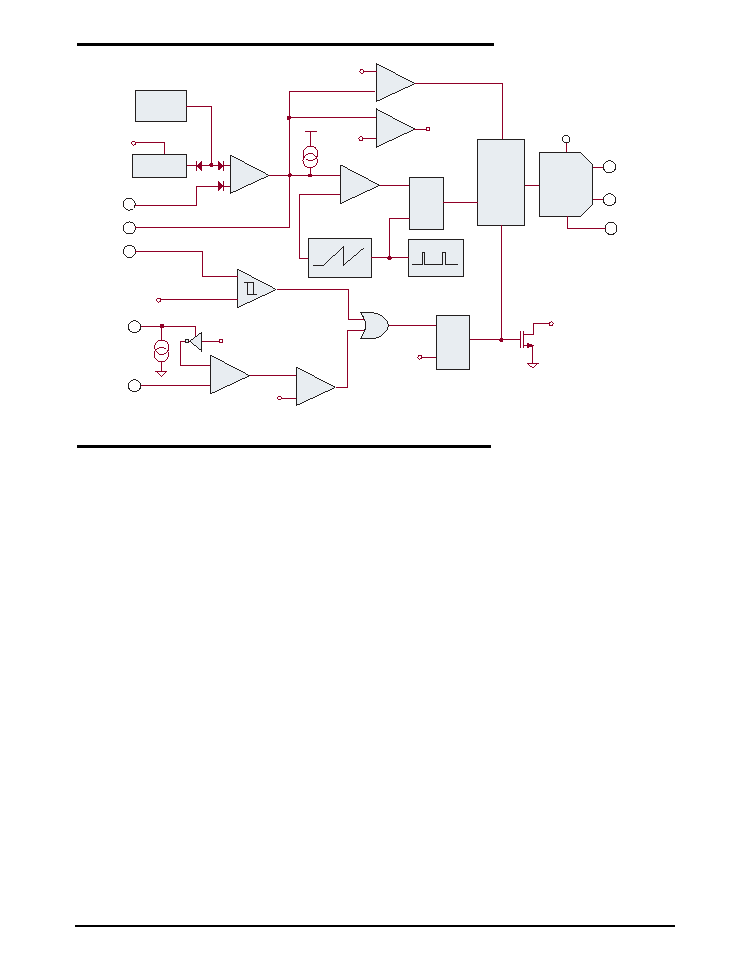
FUNCTIONAL DIAGRAM
+
-
-
+
-
+
Synchronous
Driver
PWM
Logic
S
Q
R
Reset
Dominant
S
Q
R
ISET
V
CC
ISENSE
Reference
5
4
3
6
1.25V
UVLO
FAULT
GND
2
7
NDRV
8
DRIVER ENABLE
RESET
Dominant
PWM COMP
FAULT
+
-
X 3.3
PDRV
PDRV
V
CC
5
µ
A
300mV
SHUTDOWN
GM
ERROR
AMP
Over Current
(Gated S&H)
2.79V ON
2.69V OFF
30
µ
A
(3300 ppm/
∞
C)
COMP
SHUTDOWN
F = 500kHz
750mV RAMP
0.4V/ms
SOFTSTART
V
FB
COMP
1
-
+
-
+
1V
530mV
(3300 ppm/
∞
C)
+
-
General Overview
The SP6121 is a constant frequency, voltage
mode, synchronous PWM controller designed
for low voltage, DC/DC step down converters.
It is intended to provide complete control for a
high power, high efficiency, precisely regulated
output voltage from a highly integrated 8-pin
solution.
The internal free-running oscillator accurately
sets the PWM frequency at 500kHz without
requiring any external elements and allows the
use of physically small, low value external com-
ponents without compromising performance. A
transconductance amplifier is used for the error
amplifier, which compares an attenuated sample
of the output voltage with a precision reference
voltage. The output of the error amplifier
(COMP), is compared to a 0.75V peak-to-peak
ramp waveform to provide PWM control. The
COMP pin provides access to the output of the
error amplifier and allows the use of external
components to stabilize the voltage loop.
High efficiency is obtained through the use of
synchronous rectification. Synchronous regula-
tors replace the catch diode in the standard buck
converter with a low R
DS(ON)
N-channel
MOSFET switch allowing for significant effi-
ciency improvements. The SP6121 includes two
fast MOSFET drivers with internal non-overlap
circuitry and drives a complementary pair of
power transistors, P-channel on the high side,
and N-channel on the low side. The use of a P-
channel high side device minimizes complexity
and external component count by eliminating
the need for a charge pump that would otherwise
be required to fully enhance an N-channel de-
vice. It also allows inherent 100% duty cycle for
low dropout operation in the event of a low input
supply voltage condition.
The SP6121 includes an internal 0.4V/ms soft-
start circuit that provides controlled ramp up of
the output voltage, preventing overshoot and
inrush current at power up.
Current limiting is implemented by monitoring
the voltage drop across the R
DS(ON)
of the high
side P-channel MOSFET while it is conducting,
thereby eliminating the need for an external
sense resistor. The over-current comparator has
a built-in threshold of 160mV that can be pro-
grammed to higher values using a single exter-
nal resistor, connected to the I
SET
pin, whose
THEORY OF OPERATION

Rev. 7/2/03
SP6121 Low Voltage, 8 Pin, Synchronous Buck Controller © Copyright 2003 Sipex Corporation
5
value is selected to match the MOSFET charac-
teristics. When the over-current threshold is
exceeded, the over-current comparator sets the
fault latch and terminates the output pulses. The
controller stops switching and goes through a
hiccup sequence. This prevents excessive power
dissipation in the external power MOSFETs
during an overload condition. An internal delay
circuit prevents that very short and mild over-
load conditions, that could occur during a load
transient, activate the current limit circuit.
A low power sleep mode can be invoked in the
SP6121 by externally forcing the COMP pin
below 0.3V. Quiescent supply current in sleep
mode is typically less than 25
µA. An internal
5
µA pull-up current at the COMP pin brings the
SP6121 out of shutdown mode.
The SP6121 also includes under-voltage lock-
out and over-voltage protection. Output over-
voltage protection is achieved by turning off the
high side switch, and turning on the low side N-
channel MOSFET full time.
Enable
Low quiescent mode or "Sleep Mode" is initi-
ated by pulling the COMP pin below 0.3V with
an external open-drain or open-collector tran-
sistor. Supply current is reduced to 25
µA (typi-
cal) in shutdown. On power-up, assuming that
V
CC
has exceeded the UVLO start threshold
(2.79V), an internal 5
µA pull-up current at the
COMP pin brings the SP6121 out of shutdown
mode and ensures start-up. During normal oper-
ating conditions and in absence of a fault, an
internal clamp prevents the COMP pin from
swinging below 0.6V. This guarantees that dur-
ing mild transient conditions, due either to line
or load variations, the SP6121 does not enter
shutdown unless it is externally activated.
During Sleep Mode, the high side and low side
MOSFETs are turned off and the internal soft
start voltage is held low.
UVLO
Assuming that there is not shutdown condition
present, then the voltage on the V
CC
pin deter-
mines operation of the SP6121. As V
CC
rises,
the UVLO block monitors V
CC
and keeps the
high side and low side MOSFETS off and the
internal SS voltage low until V
CC
reaches 2.79V.
If no faults are present, the SP6121 will initiate
a soft start when V
CC
exceeds 2.79V.
Hysteresis (about 100mV) in the UVLO com-
parator provides noise immunity at start-up.
Soft Start
Soft start is required on step-down controllers to
prevent excess inrush current through the power
train during start-up. Typically this is managed
by sourcing a controlled current into a timing
capacitor and then using the voltage across this
capacitor to slowly ramp up either the error amp
reference or the error amp output (COMP). The
control loop creates narrow width driver pulses
while the output voltage is low and allows these
pulses to increase to their steady-state duty
cycle as the output voltage increases to its regu-
lated value. As a result of controlling the induc-
tor volt*second product during startup, inrush
current is also controlled.
In the SP6121 the duration of the soft-start is
controlled by an internal timing circuit that
provides a 0.4V/ms slew-rate, which is used
during start-up and over-current to set the hic-
cup time. The SP6121 implements soft-start by
ramping up the error amplifier reference voltage
providing a controlled slew-rate of the output
voltage, thereby preventing overshoot and in-
rush current at power up.
The presence of the output capacitor creates
extra current draw during startup. Simply stated,
dV
OUT
/dt requires an average sustained current
in the output capacitor and this current must be
considered while calculating peak inrush cur-
rent and over current thresholds. An approxi-
mate expression to determine the excess inrush
current due to the dV
OUT
/dt of the output capaci-
tor C
OUT
is:
IC
OUT
= C
OUT
*(0.4 V/ms) *
V
OUT
1.25
As Figure 1 shows, the SS voltage controls a
variety of signals. First, provided all the exter-
nal fault conditions are removed, an internal
5
µA pull-up at the COMP pin brings the SP6121
out of shutdown mode. The internal timing
circuit is then activated and controls the ramp-
up of the error amp reference voltage. The
COMP pin is pulled to 0.7V by the internal
THEORY OF OPERATION: continued