 | –≠–ª–µ–∫—Ç—Ä–æ–Ω–Ω—ã–π –∫–æ–º–ø–æ–Ω–µ–Ω—Ç: SP6137 | –°–∫–∞—á–∞—Ç—å:  PDF PDF  ZIP ZIP |
1
Date: 7/28/04 SP6137 Wide Input, 900KHz Synchronous PWM Controll © Copyright 2004 Sipex Corporation
SP6137
FEATURES
2.5V to 20V Step Down Achieved Using Dual Input
Small 10-Pin MSOP Package
2A to 15A Ouput Capability
Highly Integrated Design, Minimal Components
UVLO Detects Both V
CC
and V
IN
Short Circuit Protection with Auto-Restart
On-Board 1.5 sink (2 source) NFET Drivers
Programmable Soft Start
Fast Transient Response
High Efficiency: Greater than 94% Possible
A Synchronous Start-Up into a Pre-Charged Output
Wide Input, 900KHz Synchronous PWM Controller
DESCRIPTION
The SP6137 is a synchronous step-down switching regulator controller optimized for high efficiency. The part is
designed to be especially attractive for dual supply, 12V step down with 5V used to power the controller. This lower V
CC
voltage minimizes power dissipation in the part. The SP6137 is designed to drive a pair of external NFETs using a fixed
900kHz frequency, PWM voltage mode architecture. Protection features include UVLO, thermal shutdown and output
short circuit protection. The SP6137 is available in the cost and space saving 10-pin MSOP
.
Æ
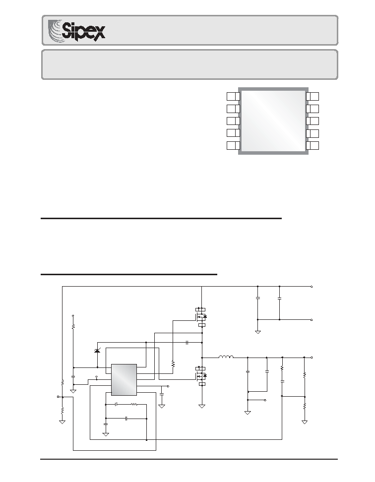
TYPICAL APPLICATION CIRCUIT
V
CC
GL
GND
V
FB
COMP
SP6137
10 Pin MSOP
1
2
3
4
5
10
9
8
7
6
BST
GH
SWN
SS
UVIN
APPLICATIONS
12V DPA
Communications Systems
Graphics Cards
Now Available in Lead Free Packaging
8 7 6 5
1 2 3
4
CSS
47nF
CBST
1µF
L1 SC5018-2R7M
2.7µH @ 12A
DCR=4.30m
FDS6676S
14.5A, 6.0m
C3
47µF
6.3V
R1
68.1k, 1%
V
OUT
VIN
1.8V @ 10A
R2
21.5k, 1%
C
VCC
10µF
6.3V
R3
221k, 1%
R4
100k, 1%
CF1
100pF
CZ2
820pF
CP1
56pF
RZ2
40.2k, 1%
FDS6676S
14.5A, 6m
8 7 6 5
4
1 2 3
DBST
MBR0530
SP6137
1
2
3
4
5
10
9
8
7
6
VCC
GL
GND
VFB
COMP
BST
GH
SWN
SS
UVIN
UV
IN
V
CC
GND 3
RLF
3.0,5%
U1
C
VCC
Ceramic
8050
X5R
QT
SS
GND2
C3, C4
Ceramic
1210
X5R
C4
47µF
6.3V
RZ3
4.64k, 1%
CZ3
220pF
C1
22µF
16V
C2
22µF
16V
GND
VIN
2.5V -20V
C1, C2
Ceramic
1210
X5R
R5
Bead
QB
= 5V @ 30mA
0.8V

2
Date: 7/28/04 SP6137 Wide Input, 900KHz Synchronous PWM Controll © Copyright 2004 Sipex Corporation
PARAMETER
MIN
TYP
MAX
UNITS
CONDITIONS
QUIESCENT CURRENT
V
CC
Supply Current
1.5
mA
V
FB
=0.9V (No switching)
BST Supply Current
0.2
0.4
mA
V
FB
=0.9V (No switching)
PROTECTION: UVLO
V
CC
UVLO Start Threshold
4.00
4.25
4.5
V
V
CC
UVLO Stop Threshold
3.80
4.05
4.4
V
V
CC
UVLO Hysteresis
200
mV
UVIN Start Threshold
2.3
2.5
2.65
V
UVIN Stop Threshold
2.0
2.2
2.35
V
UVIN Hysteresis
300
mV
ERROR AMPLIFIER REFERENCE
Error Amplifier Reference
0.792
0.800
0.808
V
2X Gain Config., Measure COMP/2
Error Amplifier Reference
0.788
0.800
0.812
V
Over Line and Temperature
Error Amplifier Transconductance
6
ms
Error Amplifier Gain
60
dB
No Load
COMP Sink Current
150
µA
V
FB
= 0.9V, COMP = 0.9V
COMP Source Current
150
µA
V
FB
= 0.7V, COMP = 2.2V
V
FB
Input Bias Current
50
200
nA
V
FB
= 0.8V
Internal Pole
4
MHz
COMP Clamp
2.5
V
V
FB
=0.7V, T
A
= 25∞C
COMP Clamp Temp. Coefficient
-2
mV/∞C
CONTROL LOOP: PWM COMPARATOR, RAMP & LOOP DELAY PATH
Ramp Amplitude
0.92
1.1
1.28
V
RAMP Offset
1.1
V
T
A
= 25∞C, RAMP COMP
until GH starts switching
RAMP Offset Temp. Coefficient
-2
mV/∞C
GH Minimum Pulse Width
90
180
ns
Maximum Controllable Duty Ratio
92
97
%
Maximum Duty Ratio Measured just
before pulse skipping begins
Maximum Duty Ratio
100
%
Valid for 20 Cycles
Internal Oscillator Frequency
810
900
990
kHz
ELECTRICAL SPECIFICATIONS
Unless otherwise specified: -40∞C < T
AMB
< 85∞C, 4.5V < V
CC
< 5.5V, BST=V
CC
,SWN = GND = 0V, UVIN = 3.0V, CV
CC
=
10µF, C
COMP
= 0.1µF, CGH = CGL = 3.3nF, C
SS
= 50nF, Typical measured at V
CC
=5V. The denotes the specifications
which apply over the full operating temperature range, unless otherwise specified.
These are stress ratings only and functional operation of the device at
these ratings or any other above those indicated in the operation sections
of the specifications below is not implied. Exposure to absolute maximum
rating conditions for extended periods of time may affect reliability.
V
CC
.................................................................................................. 7V
BST ............................................................................................... 27V
BST-SWN ......................................................................... -0.3V to 7V
SWN ................................................................................... -1V to 20V
GH ......................................................................... -0.3V to BST+0.3V
GH-SWN ......................................................................................... 7V
All other pins .......................................................... -0.3V to V
CC
+0.3V
Peak Output Current < 10us
GH,GL ............................................................................................. 2A
Storage Temperature .................................................. -65∞C to 150∞C
Power Dissipation .......................................................................... 1W
Lead Temperature (Soldering, 10 sec) ...................................... 300∞C
ESD Rating .......................................................................... 2kV HBM
Thermal Resistance ............................................................. 41.9∞C/W
ABSOLUTE MAXIMUM RATINGS

3
Date: 7/28/04 SP6137 Wide Input, 900KHz Synchronous PWM Controll © Copyright 2004 Sipex Corporation
PARAMETER
MIN
TYP
MAX
UNITS
CONDITIONS
TIMERS: SOFTSTART
SS Charge Current:
10
µA
SS Discharge Current:
1
mA
Fault Present, SS = 0.2V
PROTECTION: SHORT CIRCUIT & THERMAL
Short Circuit Threshold Voltage
0.2
0.25
0.3
V
Measured V
REF
(0.8V) - V
FB
Hiccup Timeout
100
ms
V
FB
= 0V
Number of Allowable Clock Cycles
20
Cycles
V
FB
= 0.7V
at 100% Duty Cycle
Minimum GL Pulse After 20 Cycles
0.5
Cycles
V
FB
= 0.7V
Thermal Shutdown Temperature
145
∞C
Thermal Recovery Temperature
135
∞C
Thermal Hysteresis
10
∞C
OUTPUT: NFET GATE DRIVERS
GH & GL Rise Times
35
50
ns
Measured 10% to 90%
GH & GL Fall Times
30
40
ns
Measured 90% to 10%
GL to GH Non Overlap Time
45
70
ns
GH & GL Measured at 2.0V
SWN to GL Non Overlap Time
20
30
ns
Measured SWN = 100mV to GL = 2.0V
GH & GL Pull Down Resistance
50
K
ELECTRICAL SPECIFICATIONS: Continued
Unless otherwise specified: 0∞C < T
AMB
< 70∞C, 4.5V < V
CC
< 5.5V, BST=V
CC
,SWN = GND = 0V, UVIN = 3.0V, CV
CC
= 10µF,
C
COMP
= 0.1µF, CGH = CGL = 3.3nF, C
SS
= 50nF, Typical measured at V
CC
=5V. The denotes the specifications which
apply over the full operating temperature range, unless otherwise specified.
PIN DESCRIPTION
PIN #
PIN NAME DESCRIPTION
1
V
CC
Bias Supply Input. Connect to external 5V supply. Used to power internal circuits and
low side gate driver.
2
GL
High current driver output for the low side NFET switch. It is always low if GH is high or
during a fault. Resistor pull down ensure low state at low voltage.
3
GND
Ground Pin. The control circuitry of the IC and lower power driver are referenced to this
pin. Return separately from other ground traces to the (-) terminal of C
OUT
.
4
V
FB
Feedback Voltage and Short Circuit Detection pin. It is the inverting input of the Error
Amplifier and serves as the output voltage feedback point for the Buck Converter. The
output voltage is sensed and can be adjusted through an external resistor divider.
Whenever V
FB
drops 0.25V below the positive reference, a short circuit fault is detected
and the IC enters hiccup mode.
5
COMP
Output of the Error Amplifier. It is internally connected to the non-inverting input of the
PWM comparator. An optimal filter combination is chosen and connected to this pin and
either ground or V
FB
to stabilize the voltage mode loop.
6
UVIN
UVLO input for V
IN
voltage. Connect a resistor divider between V
IN
and UVIN to set
minimum operating voltage.
7
SS
Soft Start. Connect an external capacitor between SS and GND to set the soft start rate
based on the 10µA source current. The SS pin is held low via a 1mA (min) current during
all fault conditions.
8
SWN
Lower supply rail for the GH high-side gate driver. Connect this pin to the switching node
at the junction between the two external power MOSFET transistors.
9
GH
High current driver output for the high side NFET switch. It is always low if GL is high or
during a fault. Resistor pull down ensure low state at low voltage.
10
BST
High side driver supply pin. Connect BST to the external boost diode and capacitor as
shown in the Typical Application Circuit on page 1. High side driver is connected between
BST pin and SWN pin.
4
Date: 7/28/04 SP6137 Wide Input, 900KHz Synchronous PWM Controll © Copyright 2004 Sipex Corporation
General Overview
The SP6137 is a fixed frequency, voltage mode,
synchronous PWM controller optimized for high
efficiency. The part has been designed to be
especially attractive for split plane applications
utilizing 5V to power the controller and 2.5V to
20V for step down conversion.
The heart of the SP6137 is a wide bandwidth
transconductance amplifier designed to accom-
modate Type II and Type III compensation
schemes. A precision 0.8V reference present on
the positive terminal of the error amplifier per-
mits the programming of the output voltage
down to 0.8V via the V
FB
pin. The output of the
error amplifier, COMP, compared to a 1.1V
peak-to-peak ramp is responsible for trailing
edge PWM control. This voltage ramp and PWM
control logic are governed by the internal oscil-
lator that accurately sets the PWM frequency to
900kHz.
FUNCTIONAL DIAGRAM
1.7 V
1.7 V
POWER OK ONCE LOGIC
COMPARATOR
ASYNC. STARTUP
0.4 V
THERMAL
FAULT
FAULT
CLR
COUNT 20
CLOCK
PULSES
600 kHZ
CLK
CLOCK PULSE GENERATOR
SS
GL HOLD OFF
SHUTDOWN
100% Protection Logic
Q
R
S
RESET
DOMINANT
QPWM
CLK
SYNCHRONOUS
DRIVER
GND
3
2 GL
PWM LOOP
5 COMP
POS REF
FAULT
Logic
Delay
FAULT
UVIN
6
1
7
COUNTER
CLR
V
CC
UVLO
VIN UVLO
REF OK
4.05 V OFF
4.25 V ON
2.50 V ON
2.20 V OFF
UVLO COMPARATORS
REF OK
0.25V
VPOS
VFBINT
PWRFLT
0.8V
CORE
REFERENCE
V
CC
REF OK
THERMAL AND SHORT CIRCUIT PROTECTION
FAULT
Q
145∞C ON
REF OK
100ms Delay
CLK
MFLT
DOMINANT
R
S
SET
DOMINANT
SET
Q
R
S
135∞C OFF
DETECTION
SHORT CIRCUIT
SOFTSTART INPUT
RAMP = 1.1V
VFBINT
VPOS
Gm
Gm ERROR AMPLIFIER
9 GH
8 SWN
10 BST
VFB
SS
10 µA
VCC
VCC
VCC
PWRFLT
MFLT
THEORY OF OPERATION
The SP6137 contains two unique control fea-
tures that are very powerful in distributed appli-
cations. First, asynchronous driver control is
enabled during start up to prohibit the low side
NFET from pulling down the output until the
high side NFET has attempted to turn on. Sec-
ond, a 100% duty cycle timeout ensures that the
low side NFET is periodically enhanced during
extended periods at 100% duty cycle. This guar-
antees the synchronized refreshing of the BST
capacitor during very large duty ratios.
The SP6137 also contains a number of valuable
protection features. A programmable input (V
IN
)
UVLO allows a user to set the exact value at
which the conversion voltage is at a safe point to
begin down conversion, and an internal V
CC
UVLO ensures that the controller itself has
enough voltage to properly operate. Other pro-

5
Date: 7/28/04 SP6137 Wide Input, 900KHz Synchronous PWM Controll © Copyright 2004 Sipex Corporation
tection features include thermal shutdown and
short-circuit detection. In the event that either a
thermal, short-circuit, or UVLO fault is de-
tected, the SP6137 is forced into an idle state
where the output drivers are held off for a finite
period before a re-start is attempted.
Under Voltage Lock Out (UVLO)
The SP6137 contains two separate UVLO com-
parators to monitor the bias (V
CC
) and conver-
sion (V
IN
) voltages independently. The V
CC
UVLO threshold is internally set to 4.25V,
whereas the V
IN
UVLO threshold is program-
mable through the UVIN pin. When the UVIN
pin is greater than 2.5V, the SP6137 is permitted
to start up pending the removal of all other
faults. Both the V
CC
and V
IN
UVLO compara-
tors have been designed with hysteresis to pre-
vent noise from resetting a fault.
Soft Start
"Soft Start" is achieved when a power converter
ramps up the output voltage while controlling
the magnitude of the input supply source cur-
rent. In a modern step down converter, ramping
up the positive terminal of the error amplifier
controls soft start. As a result, excess source
current can be defined as the current required to
charge the output capacitor.
IV
IN
= C
OUT
* DV
OUT
/ DTSoft-start
The SP6137 provides the user with the option to
program the soft start rate by tying a capacitor
from the SS pin to GND. The selection of this
capacitor is based on the 10uA pull up current
present at the SS pin and the 0.8V reference
voltage. Therefore, the excess source can be
redefined as:
IV
IN
= C
OUT
* DV
OUT
*10
µA / (C
SS
* 0.8V)
Hiccup
Upon the detection of a power, thermal, or short-
circuit fault, the SP6137 is forced into an idle
state for 100mS (typical). The SS and COMP
pins are immediately pulled low, and the gate
drivers are held off for the duration of the
timeout period. Power and thermal faults have
to be removed before a restart may be attempted,
whereas, a short-circuit fault is internally cleared
shortly after the fault latch is set. Therefore, a
restart attempt is guaranteed every 100mS (typi-
cal) as long as the short-circuit condition per-
sists.
Thermal and Short-Circuit
Protection
Because the SP6137 is designed to drive large
NFETs running at high current, there is a chance
that either the controller or power converter will
become too hot. Therefore, an internal thermal
shutdown (145
∞C) has been included to prevent
the IC from malfunctioning at extreme tempera-
tures.
A short-circuit detection comparator has also
been included in the SP6137 to protect against
the accidental short or sever build up of current
at the output of the power converter. This com-
parator constantly monitors the positive and
negative terminals of the error amplifier, and if
the V
FB
pin ever falls more than 250mV (typi-
cal) below the positive reference, a short-circuit
fault is set. Because the SS pin overrides the
internal 0.8V reference during soft start, the
SP6137 is capable of detecting short-circuit
faults throughout the duration of soft start as
well as in regular operation.
Error Amplifier and Voltage Loop
As stated before, the heart of the SP6137 voltage
error loop is a high performance, wide band-
width transconductance amplifier. Because of
the amplifier's current limited (+/-150
µA)
transconductance, there are many ways to com-
pensate the voltage loop or to control the COMP
pin externally. If a simple, single pole, single
THEORY OF OPERATION: Continued