 | –≠–Ľ–Ķ–ļ—ā—Ä–ĺ–Ĺ–Ĺ—č–Ļ –ļ–ĺ–ľ–Ņ–ĺ–Ĺ–Ķ–Ĺ—ā: SP6650EU | –°–ļ–į—á–į—ā—Ć:  PDF PDF  ZIP ZIP |
1
Date: 5/25/04
SP6650 High Efficiency 600mA Synchronous Buck Regulator
© Copyright 2004 Sipex Corporation
High Efficiency 600mA Synchronous Buck Regulator
Ideal for portable designs powered with Li Ion battery
SP6650
FEATURES
95% High Efficiency
Proprietary Control Loop
2.7V to 6.5V Input Voltage Range
3.3V or Adjustable Output Voltage
Range
2% Output Voltage Accuracy
600mA Output Current
100% Duty Cycle Operation
Programmable Inductor Peak Current
Limit (0.95A or 0.5A)
No External FET's Required
3V Battery Low Indicator
2.7V Undervoltage Lockout
Shutdown Control
Small 10-Pin MSOP
The SP6650 is ideal for portable applications that use a Li-Ion or 3 to 4 cell alkaline/NiCd/NiMH
input. The SP6650 extends battery life with it's unique control loop scheme (patent pending),
which maintains high efficiency levels (> than 90%) over a wide range of output currents. Features
such as Inductor peak current control, protects the power supply from overload or short circuit
conditions, controls the startup current to prevent output overshoot and excessive battery drop,
and gives the user more flexibility in choosing an appropriate coil to optimize solution cost, size
and performance. Other features include a dedicated pin for manual shutdown, a battery low
indicator, and thermal protection.
TYPICAL APPLICATIONS CIRCUIT
ģ
RB
100k
2.7-6.5 VDC
3.3V or 1.25V
to 5.0V
SP6650
10
9
8
7
6
1
2
3
4
5
R1
10
C1
1ĶF
C2
47ĶF
L1 22ĶH
V
OUT
C3
47ĶF
R2
164k
R3
100k
C4
470pF
PV
IN
V
IN
BLON
I
LIM
SHDN
LX
PGND
GND
V
OUT
FB
ģ
ģ
R4
100k
DESCRIPTION
APPLICATIONS
PDA
CD Player
ADSL Modem
Digital Still Camera
Now Available in Lead Free Packaging
PV
IN
V
IN
BLON
I
LIM
SHDN
SP6650
10 Pin MSOP
1
2
3
4
5
10
9
8
7
6
LX
PGND
GND
V
OUT
FB
2
Date: 5/25/04
SP6650 High Efficiency 600mA Synchronous Buck Regulator
© Copyright 2004 Sipex Corporation
ABSOLUTE MAXIMUM RATINGS
These are stress ratings only and functional operation
of the device at these ratings or any other above those
indicated in the operation sections of the specifications
below is not implied. Exposure to absolute maximum
rating conditions for extended periods of time may
affect reliability.
PV
IN
, V
IN
. ........................................................... 7V
All other pins .............................. -0.3V to V
IN
+0.3V
PV
IN
, PGND, LX current .................................... 2A
Storage Temperature .................... -65įC to 150įC
Lead Temperature (Soldering 10sec) .......... 300įC
Specifications apply for -40įC to +85įC, V
OUT
= 3.3V, V
IN
= 3.6V, I
LIM
= SHDN = V
IN
, FB = GND, L1 = 22ĶH, C
OUT
= C
IN
= 47ĶF, unless otherwise noted.
PARAMETER
MIN.
TYP.
MAX.
UNITS
CONDITIONS
Input Voltage Operating
UVLO
6.5
V
Range
Undervoltage Lockout Threshold
2.6
2.7
2.8
V
V
IN
Rising
Undervoltage Lockout Hysteresis
120
mV
FB Set Voltage, V
REF
1.23
1.25
1.27
V
V
OUT
tied to FB Pin
V
REF
Load Regulation
0.5
%
I
LOAD
= 0 to 600mA
V
IN
= 3.6V, V
OUT
= 3.3V
V
REF
Line Regulation
0.5
%
V
IN
= 3.6V to 6.5V
V
OUT
= 3.3V, I
LOAD
= 200mA
V
REF
Line and Load Regulation
0.65
%
V
IN
= 3.6V to 6.5V
I
LOAD
= 0 to 600mA
V
OUT
Accuracy
3.23
3.30
3.37
V
I
LOAD
= 100mA, V
IN
= 3.6V
V
OUT
Line and Load Regulation
3.17
3.30
3.43
V
V
IN
= 3.6V to 6.5V
I
LOAD
= 0 to 600mA
On-Time Constant - K
ON
2.7
Ķs*V
Minimum T
ON
= K
ON
/ (V
IN
-V
OUT
)
PMOS Switch Resistance
0.4
0.8
I
PMOS
= 200mA
NMOS Switch Resistance
0.3
0.8
I
NMOS
= 200mA
V
IN
Pin Quiescent Current
70
150
ĶA
SHDN = V
IN
= FB = 1.5V
V
IN
Pin Shutdown Current
0.3
500
nA
SHDN = 0V
V
OUT
Pin Quiescent Current
7
12
ĶA
SHDN = V
IN
= FB = 1.5V
V
OUT
Pin Shutdown Current
0.1
500
nA
SHDN = 0V
Power Efficiency
92
%
I
LOAD
= 600mA
95
%
I
LOAD
= 100mA
88
%
I
LOAD
= 1mA
Minimum Guaranteed Load
600
700
mA
I
LIM
= V
IN
Current
300
350
mA
I
LIM
= 0V
Inductor Current Limit
0.75
0.95
1.15
A
I
LIM
= V
IN
0.40
0.50
0.60
A
I
LIM
= 0V
Inductor Current Limit
-100
ppm/įC
ELECTRICAL CHARACTERISTICS
3
Date: 5/25/04
SP6650 High Efficiency 600mA Synchronous Buck Regulator
© Copyright 2004 Sipex Corporation
BLOCK DIAGRAM
SPECIFICATIONS (continued)
Specifications apply for -40įC to +85įC, V
OUT
= 3.3V, V
IN
= 3.6V, I
LIM
= SHDN = V
IN
, FB = GND, L1 = 22ĶH, C
OUT
= C
IN
= 47ĶF, unless otherwise noted.
PVIN
Internal
Supply
V
IN
Min
T
OFF
Min
T
ON
REF
SHDN
UVLO
REF
SHDN
I
LIM
FB
V
OUT
Ref
Block
REF
REF/2
I
LIM
/M
overcurrent
GND
BLON
UVLO
I
LIM
/M
D
V
IN
CLR
REF/2
Q
V
IN
Q
LX
+
-
C
+
-
C
+
-
C
+
-
C
+
-
C
M
1
PGND
TSD
V
IN
PARAMETER
MIN.
TYP.
MAX.
UNITS
CONDITIONS
Falling BLON Trip Voltage
2.88
3.00
3.12
V
BLON Trip Voltage Hysteresis
2.9
%
BLON Low Output Voltage
0.4
V
V
IN
= V
OUT
= 3.0V,
I
SINK
= 1mA
BLON Leakage Current
1
ĶA
V
BLON
= 3.3V
Rising Over-Temperature Trip
140
įC
Point
Over-Temperature Hysteresis
14
įC
SHDN, ILIM Leakage Current
1
500
nA
SHDN, ILIM Input Threshold
0.60
0.90
1.8
V
High to Low Transition
Voltage
0.60
1.25
1.8
V
Low to High Transition
4
Date: 5/25/04
SP6650 High Efficiency 600mA Synchronous Buck Regulator
© Copyright 2004 Sipex Corporation
PIN DESCRIPTION
PIN NUMBER
PIN NAME
DESCRIPTION
1
PV
IN
Input voltage power pin. Inductor charging current passes
through this pin.
2
V
IN
Internal supply voltage. Control circuitry powered from this
pin.
3
BLON
Open drain battery low output. V
IN
below battery low thresh-
old pulls this node to ground. V
IN
above threshold, this node
is open.
4
I
LIM
Inductor current limit programming pin. Tie pin to V
IN
for
0.95A peak inductor current limit. Tie pin to ground for 0.5A
peak inductor current limit. TTL input threshold.
5
SHDN
Shutdown control input. Tie to V
IN
for normal operation, tie to
ground for shutdown. TTL input threshold.
6
FB
External feedback network input connection. Connect a
resistor from FB to ground and FB to V
OUT
to control the
output voltage externally. This pin regulates to the internal
bandgap reference voltage of 1.25V. Tie FB to ground to use
the internal divider for a preset output voltage of 3.3V.
7
V
OUT
Output voltage sense pin. Used for internal feedback divider
and timing circuit.
8
GND
Internal ground pin. Control circuitry returns current to this
pin.
9
PGND
Power ground pin. Synchronous rectifier current returns
through this pin.
10
LX
Inductor switching node. Inductor tied between this pin and
the output capacitor to create regulated output voltage.

5
Date: 5/25/04
SP6650 High Efficiency 600mA Synchronous Buck Regulator
© Copyright 2004 Sipex Corporation
OPERATION
The SP6650 is a synchronous buck regulator
with an input voltage range of +2.7V to +6.5V
and an output that is either preset to +3.3V, or
adjustable between +1.25V and V
IN
. The SP6650
features a unique on-time control loop that runs
in discontinuous conduction mode (DCM) or
continuous conduction mode (CCM) using syn-
chronous rectification. Other features include
overtemperature shutdown, overcurrent protec-
tion, undervoltage lockout, digitally controlled
enable, a battery low indicator, and an external
feedback pin.
The SP6650 operates with a light load quiescent
current of 70
ĶA using a 0.4 PMOS main
switch and a 0.3
NMOS auxiliary switch. It
operates with excellent efficiency across the
entire load range, making it an ideal solution for
battery powered applications and low current
step-down conversions. The part smoothly tran-
sitions into a 100% duty cycle under heavy load/
low input voltage conditions.
On-Time Control
The SP6650 uses a precision comparator and a
minimum on-time one-shot to regulate the out-
put voltage and control the inductor current
under normal load conditions. As the feedback
node (negative terminal of the loop comparator)
drops below the reference, the loop comparator
output goes high and closes the main switch.
The minimum on-time one shot is triggered,
setting a logic high for the duration defined by:
T
ON
=
K
ON
V
IN
-V
OUT
where:
K
ON
= 2.7
Ķs*V constant
V
IN
= V
IN
pin voltage
V
OUT
= V
OUT
pin voltage
The outputs of the loop comparator and the on-
time one shot are OR'd together, inverted, and
buffered to drive the gate of the high side PMOS
main switch. Increasing inductor current causes
the output to increase through the ESR (equiva-
lent series resistance) of the output capacitor. As
V
OUT
rises above the regulation threshold, the
loop comparator output resets low. Termination
of the on cycle occurs when both the loop
comparator and the on-time one shot goes to
logic low, or the inductor current limit has been
reached.
The discharge phase follows with the high side
PMOS switch opening and the low side NMOS
switch closing to provide a discharge path for
the inductor current. The decreasing inductor
current and the load current cause the output
voltage to droop. Under normal load conditions
when the inductor current is below the pro-
grammed limit, the off-time will continue until
the output voltage falls below the regulation
threshold, which initiates a new charge cycle via
the loop comparator.
The inductor current "floats" in continuous con-
duction mode. During this mode the inductor
peak current is below the programmed limit and
the valley current is above zero. This is to satisfy
load currents that are greater than half the mini-
mum current ripple. The current ripple, I
LR
, is
defined by the equation:
I
LR
K
ON
* V
IN
-V
OUT
-I
OUT
*Rch
L
V
IN
-V
OUT
where:
L
= Inductor value
I
OUT
= Load current
Rch = PMOS on resistance, 0.4
typ.
If the I
OUT
*Rch term is negligible compared
with (V
IN
-V
OUT
), the above equation simplifies
to:
I
LR
K
ON
L
For most applications, the inductor current ripple
controlled by the SP6650 is constant regardless
of input and output voltage. Because the output
voltage ripple is equal to:
V
OUT
(ripple) = I
LR
*R
ESR
where:
R
ESR
= ESR of the output capacitor
the output ripple of the SP6650 regulator is
independent of the input and output voltages.
For battery powered applications, where the
battery voltage changes significantly, the SP6650
provides constant output voltage ripple through-
out the battery lifetime. This greatly simplifies
the LC filter design.

6
Date: 5/25/04
SP6650 High Efficiency 600mA Synchronous Buck Regulator
© Copyright 2004 Sipex Corporation
R
DS(ON)
of the P-Channel MOSFET and R
L
is
the DC resistance of the inductor.
The on-time control circuit seamlessly operates
the converter between CCM, DCM, and low
dropout modes without the need for compensa-
tion. The converter's transient response is quick
since there is no compensated error amplifier in
the loop.
Inductor Over-Current Protection
The inductor over-current protection circuitry is
programmed to limit the peak inductor current
to 950mA (pin 4 tied to V
IN
) or 500mA (pin 4 to
ground). This is done during the on-time by
comparing the source to drain voltage drop of
the PMOS passing the inductor current with a
second voltage drop representing the maximum
allowable inductor current. As the two voltages
become equal, the over-current comparator trig-
gers a minimum off-time one shot. The off-time
one shot forces the loop into the discharge phase
for a minimum time causing the inductor current
to decrease.
At the end of the off-time loop, control is handed
back to the OR'd on-time signal. If the output
voltage is still low, charging begins until the
output is in regulation or the current limit has
been reached again. During startup and over-
load conditions, the converter behaves like a
current source at the programmed limit minus
half the current ripple. The minimum T
OFF
is
6
Ķs (typ.) at V
OUT
= 0V and 2
Ķs (typ.) for V
OUT
greater than 1.5V.
Under-Voltage Lockout
The SP6650 is equipped with under-voltage
lockout to protect the input battery source from
excessive currents when substantially dis-
charged. When the input supply is below the
UVLO threshold both power switches are open
to prevent inductor current from flowing. The
internal reference and regulator circuitry are
enabled drawing the 70
ĶA light load quiescent
current on pin 2. The rising input voltage UVLO
threshold is +2.7V, with a typical hysteresis of
120mV to prevent chattering due to the imped-
ance of the input source.
On-Time Control: continued
The maximum loop frequency in CCM is de-
fined by the equation:
F
LP
(V
IN
-V
OUT
)*(V
OUT
+I
OUT
*Rdc)
K
ON
*[V
IN
+I
OUT
*(Rdc-Rch)]
where:
F
LP
= CCM loop frequency
Rdc = NMOS on resistance, 0.3
typ.
Ignoring conduction losses simplifies the loop
frequency to
F
LP
=
1
*
V
OUT
* (V
IN
-V
OUT
)
K
ON
V
IN
OR'ing the loop comparator and the on-time one
shot reduces the switching frequency for load
currents below half the inductor ripple current.
This increases light load efficiency. The mini-
mum on-time insures that the inductor current
ripple is a minimum of K
ON
/L, more than the
load current demands. The converter goes in to
a standard pulse frequency modulation (PFM)
mode where the switching frequency is propor-
tional to the load current.
Low Dropout and Load Transient
Operation
OR'ing the loop comparator also increases the
duty ratio past the ideal D=V
OUT
/V
IN
up to and
including 100%. Under a light to heavy load
transient, the loop comparator will hold the
main switch on past the on-time one shot pulse
until the output is brought back into regulation.
Also, as the input voltage supply drops down
close to the output voltage, the main MOSFET
resistance loss will dictate a much higher duty
ratio to regulate the output. Eventually as the
input voltage drops low enough, the output
voltage will follow, causing the loop compara-
tor to hold the converter at 100% duty cycle.
This mode is critical in extending battery life
when the output voltage is at or above the
minimum usable input voltage. The dropout
voltage is the minimum (V
IN
- V
OUT
) below
which the output regulation cannot be main-
tained. The dropout voltage of SP6650 is equal
to I
L
(0.4
+ R
L
) where 0.4
is the typical

7
Date: 5/25/04
SP6650 High Efficiency 600mA Synchronous Buck Regulator
© Copyright 2004 Sipex Corporation
Under-Current Detection
The synchronous rectifier is comprised of the
inductor discharge switch, a voltage compara-
tor, and a latch. During the off-time, positive
inductor current flows into the PGND pin 9
through the low side NMOS switch to LX pin
10, through the inductor and the output capaci-
tor, and back to pin 9. The comparator monitors
the voltage drop across the discharge NMOS.
As the inductor current approaches zero, the
channel voltage sign goes from negative to
positive, causing the comparator to trigger the
latch and open the switch to prevent inductor
current reversal. This circuit along with the on-
time one shot puts the converter into PFM mode
and improves light load efficiency when the
load current is less than half the inductor ripple
current defined by K
ON
/L.
Thermal Shutdown
The converter will open both power switches if
the die junction temperature rises above 140
įC.
The die must cool down below 126
įC before the
regulator is re-enabled. This feature protects the
SP6650 and surrounding circuitry from exces-
sive power dissipation due to fault conditions.
Shutdown/Enable Control
Pin 5 of the device is a logic level control pin that
shuts down the converter with a logic low, or
enables the converter with a logic high. When
the converter is shut down, the power switches
are opened and all circuit biasing is extinguished
leaving only junction leakage currents on sup-
ply pins 1 and 2. After pin 5 is brought high to
enable the converter, there is a turn on delay to
allow the regulator circuitry to re-establish it-
self. Power conversion begins with the assertion
of the internal reference ready signal which
occurs approximately 150
Ķs after the enable
signal is received.
Battery Low Indicator
The regulator bias voltage on pin 2 (V
IN
) is
divided down and compared to the internal
+1.25V reference voltage. When pin 2 voltage
drops below +3.00V, an open drain NMOS on
pin 3 (BLON) sinks current to ground. Tying a
resistor from pin 3 to V
IN
or V
OUT
creates a logic
level battery low indicator. A low bandwidth
comparator and 2.9% hysteresis filter the input
voltage ripple to prevent noisy transitions at the
threshold.
External Feedback Pin
The SP6650 comes with a factory preset output
voltage of +3.3V when pin 6 (FB) is grounded.
Otherwise, the output voltage can be externally
programmed within the range +1.25V to +5.0V
by tying a resistor from FB to ground and FB to
V
OUT
(pin7). See the applications section for
resistor selection information.
8
Date: 5/25/04
SP6650 High Efficiency 600mA Synchronous Buck Regulator
© Copyright 2004 Sipex Corporation
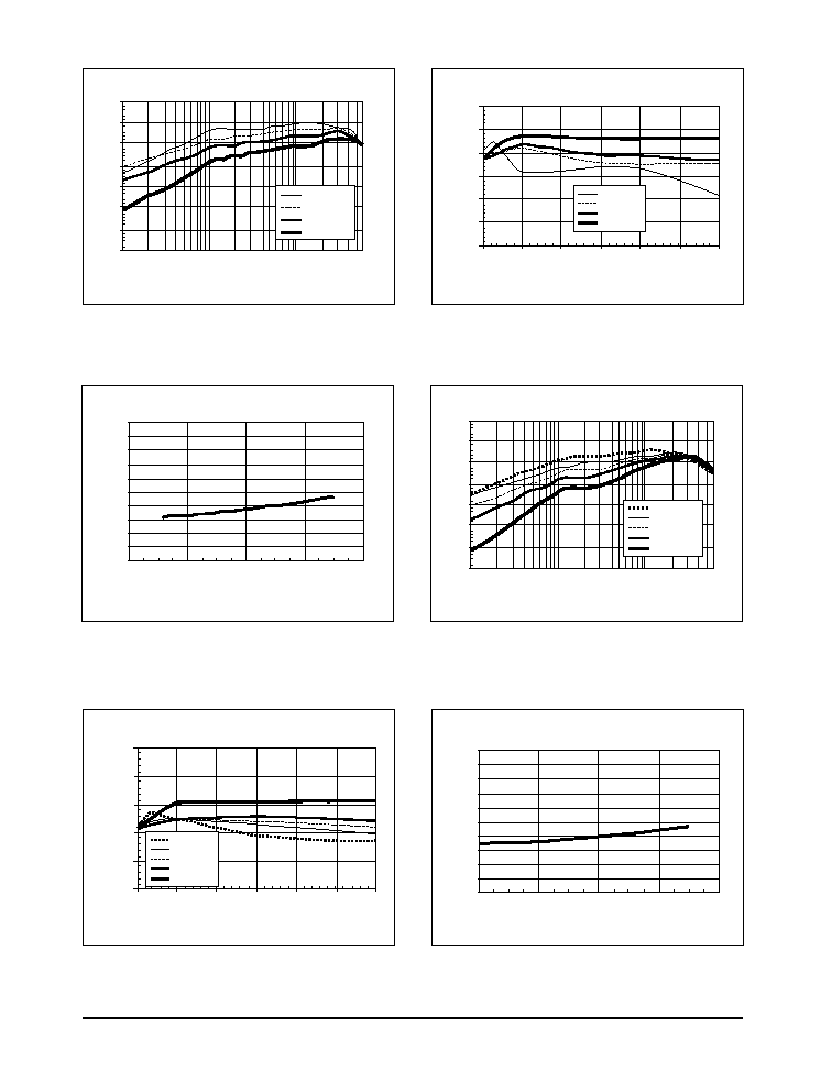
TYPICAL PERFORMANCE CHARACTERISTICS
Figure 1. Efficiency vs. Output Current, V
OUT
= 3.3V,
L1 = 22
ĶH (Sumida CDRH6D28), I
LIM
= V
IN
Figure 2. Line/Load Rejection, V
OUT
= 3.3V, L1 = 22
ĶH
(Sumida CDRH6D28), I
LIM
= V
IN
Figure 3. No Load Battery Current, V
OUT
= 3.3V,
L1 = 22
ĶH (Sumida CDRH6D28), I
LIM
= V
IN
Figure 4. Efficiency vs. Output Current, V
OUT
= 2.5V,
L1 = 22
ĶH (Sumida CDRH6D28), I
LIM
= V
IN
Figure 5. Line/Load Rejection, V
OUT
= 2.5V,
L1 = 22
ĶH (Sumida CDRH6D28), I
LIM
= V
IN
Figure 6. No Load Battery Current, V
OUT
= 2.5V,
L1 = 22
ĶH (Sumida CDRH6D28), I
LIM
= V
IN
0
3.320
3.330
3.340
3.350
3.360
3.370
3.380
V
OUT
I
LOAD
(mA)
100
200
300
400
500
600
V
IN
= 3.67V
V
IN
= 4.2V
V
IN
= 5.0V
V
IN
= 6.5V
0
20
40
60
80
100
120
140
160
180
200
3.0
4.0
5.0
6.0
7.0
V
IN
I
IN
(
Ķ
A)
100
65
70
75
80
85
90
95
1.0
10.0
100.0
600.0
Iload (mA)
Efficiency (%)
V
IN
= 3.6V
V
IN
= 4.2V
V
IN
= 5.0V
V
IN
= 6.5V
V
IN
= 3.0V
0
2.445
2.455
2.465
2.475
2.485
2.495
V
OUT
Iload (mA)
100
200
300
400
500
600
V
IN
= 3.6V
V
IN
= 4.2V
V
IN
= 5.0V
V
IN
= 6.5V
V
IN
= 3.0V
0
20
40
60
80
100
120
140
160
180
200
3.0
4.0
5.0
6.0
7.0
V
IN
I
IN
(
Ķ
A)
100
65
70
75
80
85
90
95
1.0
10.0
100.0
600.0
Iload (mA)
Efficiency (%)
V
IN
= 3.0V
V
IN
= 4.2V
V
IN
= 5.0V
V
IN
= 6.5V
9
Date: 5/25/04
SP6650 High Efficiency 600mA Synchronous Buck Regulator
© Copyright 2004 Sipex Corporation
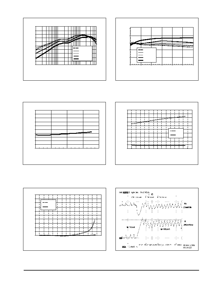
TYPICAL PERFORMANCE CHARACTERISTICS
Figure 7. Efficiency vs. Output Current, V
OUT
= 1.25V,
L1 = 22
ĶH (Sumida CDRH6D28), I
LIM
= V
IN
Figure 8. Line/Load Rejection, V
OUT
= 1.25V, L1 = 22
ĶH
(Sumida CDRH6D28), I
LIM
= V
IN
Figure 9. No Load Battery Current, V
OUT
= 1.25V,
L1 = 22
ĶH (Sumida CDRH6D28), I
LIM
= V
IN
Figure 10. Quiescent Current vs. Temperature.
V
IN
= 3.6V, SHDN = V
IN
(Enabled)
Figure 11. Quiescent Current vs. Temperature.
V
IN
= 3.6V, SHDN = GND (Shutdown)
Figure 12. Load Step Transient Response, V
OUT
= 2.5V,
10mA to 500mA. L1 = 22
ĶH (Sumida CDRH6D28),
I
LIM
= V
IN
50
55
60
65
70
75
80
85
90
95
100
1.0
10.0
100.0
600.0
Iload (mA)
Efficiency (%)
V
IN
= 3.6V
V
IN
= 4.2V
V
IN
= 5.0V
V
IN
= 6.5V
V
IN
= 3.0V
0
20
40
60
80
100
120
140
160
180
200
3.0
4.0
5.0
6.0
7.0
V
IN
I
IN
(
Ķ
A)
0
V
OUT
Iload (mA)
100
200
300
400
500
600
1.267
1.272
1.277
1.282
1.287
1.292
V
IN
= 3.6V
V
IN
= 4.2V
V
IN
= 5.0V
V
IN
= 6.5V
V
IN
= 3.0V
0
10
20
30
40
50
60
70
80
90
100
Temperature (įC)
I
Q
OP (
Ķ
A)
-50
-30
-10
-40
-20
0
20
40
10
30
60
80
50
70
100
90
I
IN
I
OUT
0
10
20
30
40
50
I
Q
sd (nA)
-50
-30
-10
-40
-20
0
20
40
10
30
60
80
50
70
100
90
I
IN
I
OUT
Temperature (įC)
10
Date: 5/25/04
SP6650 High Efficiency 600mA Synchronous Buck Regulator
© Copyright 2004 Sipex Corporation
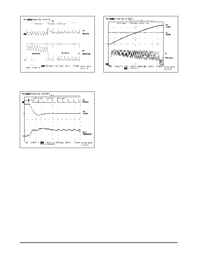
Figure 13. Load Step Transient Response, V
OUT
= 2.5V,
500mA to 10mA. L1 = 22
ĶH (Sumida CDRH6D28),
I
LIM
= V
IN
Figure 14. Low I
LIM
Startup, V
IN
= 4.2V, V
OUT
= 3.3V. I
LIM
tied to GND, Internal Feedback R
LOAD
= 33
.
Figure 15. Dead Short. V
IN
= 5.0V, I
LIM
tied to GND.
Start I
OUT
= 37mA, V
OUT
= 3.3V. Finish I
OUT
= 500mA,
V
OUT
= 20mV.

11
Date: 5/25/04
SP6650 High Efficiency 600mA Synchronous Buck Regulator
© Copyright 2004 Sipex Corporation
External Component Selection
Inductor
According to the pulse frequency modulation
(PFM) algorithm, the peak to peak output ripple
current can be calculated as:
I
LR
K
ON
L
K
ON
= 2.7
Ķs*V is a constant for SP6650 and is
set by the parameters of the internal ON-time
calculation circuitry. For the recommended 22
ĶH
inductor, typical ripple currents are I
LR
= 123mA
in discontinuous conduction mode (DCM) op-
eration. During continuous conduction mode,
the speed of the loop comparator determines the
current ripple. It is approximately equal to 200mA
with a 22
ĶH inductor.
The value of the inductor is chosen based on the
constant K
ON
and acceptable current ripple. Two
additional inductor parameters are important: its
current rating and its DC resistance.
When the current through the inductor reaches
the level of I
sat
, inductance drops down to 70%
from the nominal. This non-linear change can
cause stability problems or excessive fluctuation
in current ripple. To avoid this, the inductor
should be chosen with saturation current at least
equal to the maximum output current of the
converter plus half of the ripple. To provide the
best converter performance in dynamic condi-
tions such as start-up and load transients, induc-
tors with saturation current close to the chosen
I
LIM
are recommended.
The second important inductor parameter, DC
resistance, directly defines the efficiency of the
converter, therefore, the inductor should be cho-
sen with the minimum possible DC resistance
for a particular design. Recommended types of
the inductors for different applications are given
in Table 1. Preferred inductors for on board
power supplies with the SP6650 converter are
shielded inductors to minimize radiated mag-
netic fields emissions.
APPLICATION INFORMATION
All components recommended for typical de-
signs like those shown in the applications sche-
matics are given in Table 1.
Input and Output Capacitors
Output capacitor is often selected based on the
requirement on the output ripple voltage. In a
Buck regulator, the output ripple is determined
by ESR (equivalent series resistor) of the output
capacitors and inductor ripple current
V
OR
= ESR * I
LR
,
where V
OR
= peak to peak output ripple voltage.
SP6650's adaptive on-time scheme provides a
constant inductor ripple that is independent of
input voltages and thus makes it easier to select
the output capacitor. In many power supply
designs, the ripple voltage needs to be less than
3% of the DC output voltage. Using low ESR
tantalum or electrolytic capacitors to reduce the
output ripple.
Due to the nature of the PFM control, certain
output ripple is required for stable operation.
The loop comparator requires minimum of 15mV
ripple on the FB pin to reliably toggle the com-
parator output. That translates to an output ripple
of
V
OR(MIN)
= 15mV * V
OUT
V
REF
where V
REF
= 1.25V is the internal reference
voltage.
To reduce the output ripple and improve stabil-
ity, a small capacitor can be paralleled with the
feedback voltage divider as shown on page 1
.
This capacitor forms a high pass filter with
feedback resistor to increase the ripple voltage
seen by the FB pin. The value of the capacitor
should be in the range of 100pF to 500pF.
Although the 3.3V output can be programmed
simply by connecting the FB pin to the ground,
using this external feedback scheme can signifi-
cantly reduce the output ripple. For output ripple
less than 15mV, for instance when ceramic
capacitors are used, an artificial ramp can be
generated and superimposed onto the output.
12
Date: 5/25/04
SP6650 High Efficiency 600mA Synchronous Buck Regulator
© Copyright 2004 Sipex Corporation
TABLE 1.
DESIGNATION
DESCRIPTION
MANUFACTURER
PART NUMBER
COMMENTS
22ĶH/0.77Arms/0.104DCR
TDK
SLF7030T-220MR86
SHIELDED
INDUCTOR
22ĶH/1.1Arms/0.071DCR
MURATA
LQS66C220M04
L1
22ĶH/0.095DCR
SUMIDA
CDRH6D28
SHIELDED
47ĶH/0.76Arms/0.15DCR
MURATA
LQS66C470M04
SHIELDED
47ĶH/0.72Arms/0.37DCR
SUMIDA
CR54
C2, C3
47ĶF/350m/500mA
NEMCO
LSR47/10C-350
INPUT, OUTPUT 47ĶF/350m/500mA
AVX
TPSC476010R0350
FILTER
33ĶF/375m/542mA
AVX
TPSC336010R0375
CAPACITORS
22ĶF/700m/348mA
AVX
TPSB226010R0700
R2,R3
100K/63mW/1%Tolerance
Any approved
Any Package:
R1
10/63mW/5%Tolerance
0402,0505,0603 etc.
The schematic and description is shown in Ad-
ditional Application Circuits.
Another function of the output capacitor is to
hold up the output voltage during the load tran-
sient, and thus prevent excessive overshoot and
undershoot. For that, the recommended capaci-
tor value is greater than 22uF.
An input capacitor can reduce the peak current
drawn from the battery, improve efficiency, and
significantly reduce high frequency noises in-
duced by a switching power supply. The appli-
cable capacitors are tantalum, electrolytic and
ceramic capacitors. An RC filter is recommended
on the Vin pin (pin 2) to effectively cut down the
noise which can impact the IC control circuit.
The time constant of the RC filter needs to be at
least 5 times higher than the switching period,
calculated as 1/F
LP
during CCM.
APPLICATION INFORMATION
Output Voltage Program
The output voltage can be programmed by the
external voltage divider as shown on page 1.
First pick a resistor value less than 100k for R3.
A large R3 value would reduce the AC voltage
seen by the loop comparator because the FB pin
capacitance (can be as high as 10pF) can form a
low pass filter with R3 paralleling with R2. Lack
of AC voltage to the loop comparator would
give rise to pulse jittering and higher output
ripple. Once the R3 value is picked, R2 can be
calculated from
R
2
=
(
V
OUT
- 1
)
R
3
V
REF
13
Date: 5/25/04
SP6650 High Efficiency 600mA Synchronous Buck Regulator
© Copyright 2004 Sipex Corporation
The additional Rf/Cf network used in Figure 16
generates an artificial ramp from the LX pin
voltage and superimposes it to the feedback pin.
As a result, the internal loop comparator doesn't
have to rely on output ripple to run PFM. Now
low ESR output capacitors, such as ceramic
capacitors, can be used, and the output ripple can
be reduced by two to three times. For the best
result, size the Cf and Rf values so the network
would introduce 10 to 30mV ripples to the FB
RB
100k
SP6650
U1
10
9
8
7
6
1
2
3
4
5
L1 22ĶH
C
OUT
47ĶF
R2
160k
R3
100k
Cf
33nF
PV
IN
V
IN
BLON
I
LIM
SHDN
LX
PGND
GND
V
OUT
FB
ģ
ģ
Rf
4.99k
3.3V/600mA
Vin 2.7-6.5 VDC
CV
IN
1.0ĶF
RV
IN
10.0
C
IN
47ĶF
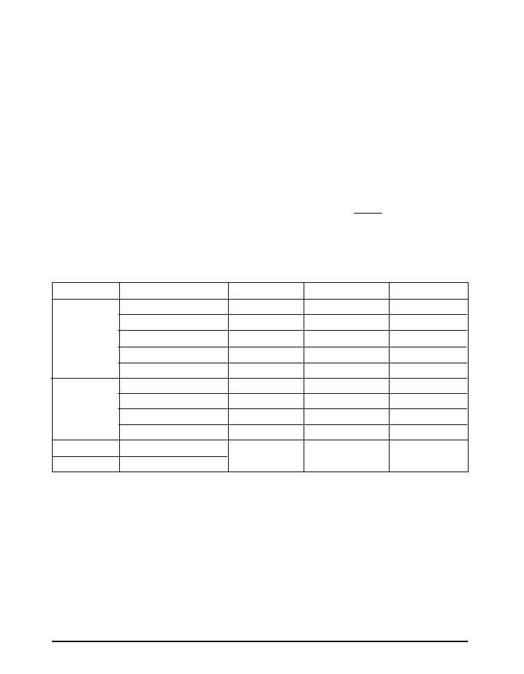
ADDITIONAL APPLICATION CIRCUITS
Figure 16. Additional Application Circuit with Low Output Ripple
pin. Oversized ripple would compromise the
load regulation and also cause oscillation during
load transient. Load transient response and out-
put ripples from Figure 16 circuit are shown in
Figure 17 and Figure 18, respectively. The added
ripple voltage can be calculated from
V =
K
ON
RfCf
Figure 17. V
OUT
transient response from 50mA to
500mA load step. CH1- V
OUT
, CH4 - I
LOAD
Figure 18. Output ripple CH1-output ripple. V
IN
= 5,
V
OUT
= 3.3V, I
LOAD
= 600mA
14
Date: 5/25/04
SP6650 High Efficiency 600mA Synchronous Buck Regulator
© Copyright 2004 Sipex Corporation
Figure 19. Additional Application Circuit: V
IN
= 5.0V, V
OUT
= 12V, and Max I
LOAD
= 150mA.
RB
100k
SP6650
U1
10
9
8
7
6
1
2
3
4
5
L3
47ĶH
COUT1
100ĶF/16V
R2
86k
R3
10k
PV
IN
V
IN
BLON
I
LIM
SHDN
LX
PGND
GND
V
OUT
FB
ģ
ģ
12V/150mA
V
IN
4.5-6.5 VDC
RV
IN
5.0
R2
4.02k
C
IN
47ĶF
D1
MBR0530TI
Q1
FDS637AN
R1
11.3k
CV
IN
1.0ĶF
Figure 20. Additional Application Circuit: V
IN
= 5.0V, V
OUT
= 5.0V, I
LOAD
= 250mA.
RB
100k
SP6650
U1
10
9
8
7
6
1
2
3
4
5
L1
47ĶH
C
OUT1
47ĶF
R2
30.9k
R3
10.2k
PV
IN
V
IN
BLON
I
LIM
SHDN
LX
PGND
GND
V
OUT
FB
ģ
ģ
5V/250mA
V
IN
4.5-6.5 VDC
RV
IN
10.0
R2
4.02k
C
IN
47ĶF
D1
MBR0530T1
Q1
FDS637AN
Cf2
470pF
R1
11.3k
CV
IN
4.7ĶF
C
OUT2
47ĶF
SP6650 can also be configured with few external
components to achieve buck-boost voltage con-
version. Efficiency of 75% to 87% can often be
obtained depending on the load current and output
voltage. Figure 19 and Figure 20 demonstrate two
typical applications in which the USB input is
converted to a 12V and a well regulated 5V.
The operation of the circuit is as follows. When
the internal high side PMOS turns on, the LX pin
swings to the input voltage which turns on the
external NMOS Q1. A voltage equal to Vin is
then applied to the inductor to cause the inductor
current rise linearly. Since there's no current
delivered to the output, the output capacitor is
discharged by the load current. Therefore, the
internal PMOS can be only turned off by the
over-current comparator since the loop com-
parator would never toggle during this state.
When the internal PMOS is open, the internal
low side NMOS is turned on. This pulls the LX
pin to the ground and turns off the Q1. As a
ADDITIONAL APPLICATION CIRCUITS: continued
result, the Schottky D2 is forward biased and
conducts the inductor current to the output. Now
the inductor experiences a reversed voltage equal
to Vout and its current ramps down linearly. As
expressed in the Operation section under In-
ductor Over-Current Protection, a minimum
T
OFF
timer is activated after the over-current
comparator is triggered in the previous state.
Before Toff expires, the internal PMOS will not
turn on, and the inductor will not be recharged
even when the output voltage drops below the
regulation voltage. This reduces the maximum
load current that can be delivered by this circuit.
Since T
OFF
is reverse proportional to the V
OUT
pin voltage, the V
OUT
pin is pulled up using a
voltage divider tying to the input voltage. As a
result, a 5V to 12V conversion can provide
maximum 120mA load. This buck-boost circuit
can regulate an output voltage higher, lower or
equal to the input voltage.
15
Date: 5/25/04
SP6650 High Efficiency 600mA Synchronous Buck Regulator
© Copyright 2004 Sipex Corporation
Layout Considerations
Proper layout is a very important part of the on-
board power supply, affecting normal function-
ality of the DC-DC converter itself and EMI.
Because of the high frequency switching of the
converter, the traces that couple an electric field
can conduct currents under the AC voltages
across the parasitic capacitance. Magnetic field
coupling traces can induce currents like trans-
formers.
To avoid an excessive interference between the
converter and the other active components on the
board, some rules should be followed.
Avoid injecting noise into the sensitive part of
the circuit via the GND Plane. Input and output
capacitors conduct the current through the GND
Plane and high frequency components of the
current can degrade the sensitive circuitry. Sepa-
rate the power and signal grounds and connect
them at one point to minimize the noise injected
from the power ground to the signal ground.
"Star" connection of the ground traces is shown
on Figure 26, where GND is the minus pole of the
output capacitor.
Power loops on the input and output of the
converter should be laid out with the shortest and
widest traces possible. The longer and narrower
the trace, the higher the resistance and induc-
tance it will have. The AC current in long traces
radiates EMI noise affecting the sensitive cir-
cuits. The length of traces in series with the
capacitors increases its ESR and ESL and reduc-
ing their effectiveness at high frequencies. There-
fore put the input capacitor as close to the appropri-
ate pins of the converter as possible and output
capacitor close to the inductor.
The external voltage feed back network should
be placed very close to the FB pin as well as
bypass capacitor C4. Any noise traces like the Lx
pin should be kept away from the voltage feed
back network and separated from it by using
power ground copper to minimize EMI.
Figure 21. Application circuit with highlighted power traces.
GND_ SIGNAL
FB
SDN
GND
PGND
BLON
V
OUT
V
IN
I
LIM
PV
IN
L
X
SP6650
2.7 - 6.5V DC
C1
1ĶF
C2
47ĶF
+
R1
10
C4
470pF
R2
100k
R3
100k
47ĶF
C3
+
2.5V
1
2
3
4
5
6
7
8
9
10
3
1
L1
22ĶH
100k
16
Date: 5/25/04
SP6650 High Efficiency 600mA Synchronous Buck Regulator
© Copyright 2004 Sipex Corporation
(ALL DIMENSIONS IN MILLIMETERS)
PACKAGE: 10-PIN MSOP
0.07 - -
L1
L
R1
ō
ō1
R
1
ō1
Seating Plane
1
E1
2
E/2
e1
e
E
D
Gauge Plane
L2
D
A2
A
A1
b
- - 1.1
0 - 0.15
Dimensions in (mm)
10-PIN MSOP
JEDEC MO-187
(BA) Variation
0.75 0.85 0.95
0.17 - 0.27
0.08 - 0.23
3.00 BSC
4.90 BSC
3.00 BSC
0.4 0.60 0.80
0.95
- 0.25 -
- 10 -
0.07 - -
0ļ 8ļ
A
A1
A2
b
c
D
E
E1
L
L1
L2
N
R
R1
ō
0ļ - 15ļ
ō1
MIN NOM MAX
e1
e
2.00 BSC
0.50 BSC
c
WITH PLATING
BASE METAL
(b)
-
-
Pin #1 indentifier must be indicated within this shaded area (D/2 * E1/2)
17
Date: 5/25/04
SP6650 High Efficiency 600mA Synchronous Buck Regulator
© Copyright 2004 Sipex Corporation
Part Number
Temperature Range
Package Type
SP6650EU .............................................. -40įC to +85įC ........................................ 10-pin MSOP
SP6650EU/TR ........................................ -40įC to +85įC ........................................ 10-pin MSOP
ANALOG EXCELLENCE
Sipex Corporation reserves the right to make changes to any products described herein. Sipex does not assume any liability arising out of the
application or use of any product or circuit described herein; neither does it convey any license under its patent rights nor the rights of others.
Corporation
Sipex Corporation
Headquarters
S233 South Hillview Drive
Milpitas, CA 95035
TEL: (408) 934-7500
FAX: (408) 935-7600
/TR = Tape and Reel
Pack quantity is 2500 for MSOP.
Available in lead free packaging. To order add "-L" suffix to part number.
Example: SP6650EU/TR = standard; SP6650EU-L/TR = lead free
ORDERING INFORMATION