 | –≠–ª–µ–∫—Ç—Ä–æ–Ω–Ω—ã–π –∫–æ–º–ø–æ–Ω–µ–Ω—Ç: SP6650UEB | –°–∫–∞—á–∞—Ç—å:  PDF PDF  ZIP ZIP |
Rev. 3/23/01
SP6650 Evaluation Board Manual
© Copyright 2001 Sipex Corporation
1
DESCRIPTION
s
High efficiency synchronous step-
down converter with up to 95%
efficiency
s
Ideal for cellular telephones, wireless
modems, PDAs, digital cameras
s
Programmable inductor peak current
limit, 2.7V-6.5V input voltage range
s
MSOP package & SMT components
for small, low profile power supply
s
Easy evaluation for different distrib-
uted power systems and battery-
powered portable equipment
SP6650 Evaluation
Board Manual
Æ
The SP6650 Evaluation Board is designed to help the user evaluate the performance of the
SP6650 for use as a single Li-Ion battery input to +5V output DC-DC Converter. The SP6650
operates from 2.7V to 6.5V input, with the highest efficiency in the range 3.0V to 4.2V where the
Li-Ion battery has the most energy. The SP6650UEB evaluation board is a complete power
supply circuit to provide ease of evaluation for the DC/DC Converter performance.
The evaluation board is a completely assembled and tested surface mount board which provides
easy probe access points to all SP6650 inputs and outputs so that the user can quickly connect
and measure electrical characteristics and waveforms.
The next two sections describe the SP6650 board layout and using the SP6650 evaluation
boards. A table of SP6650 pin assignments is also included with details on input/output pin
function. A SP6650 evaluation board list of materials table is provided with some manufacturers
part numbers to use as a reference. Finally, a schematic and drawings of the PC layout are
included as a design-in tool for the user of the SP6650.
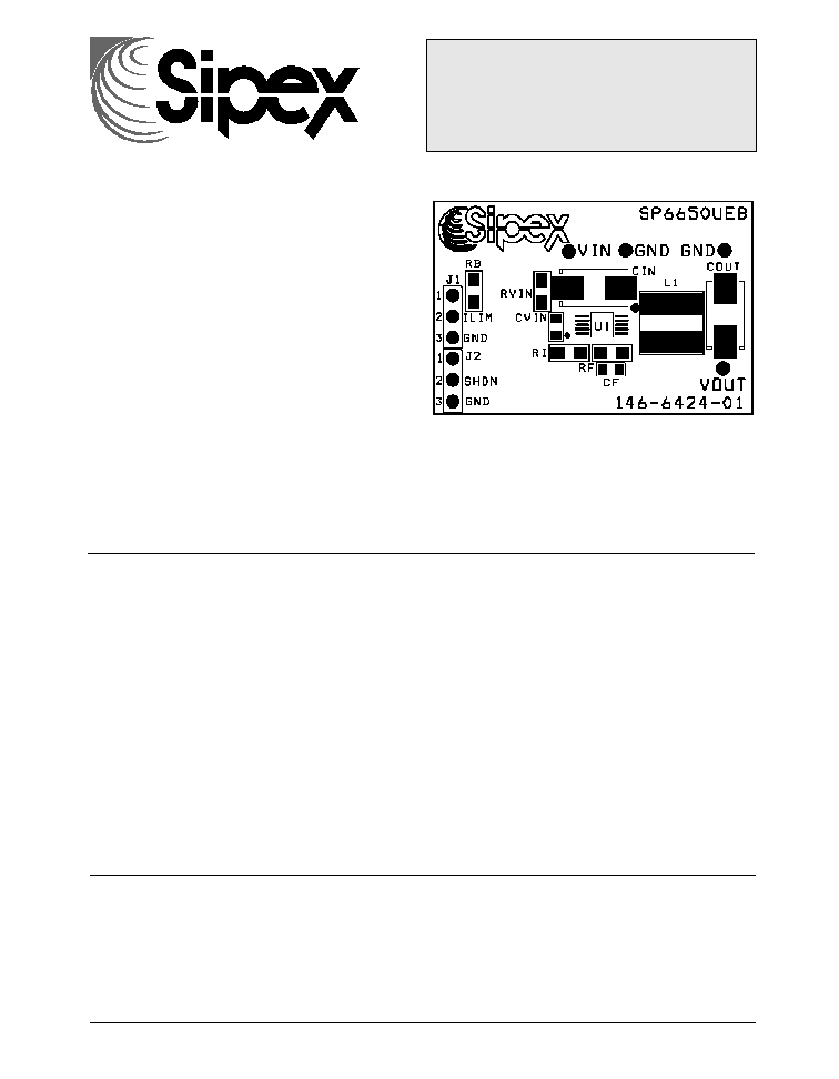
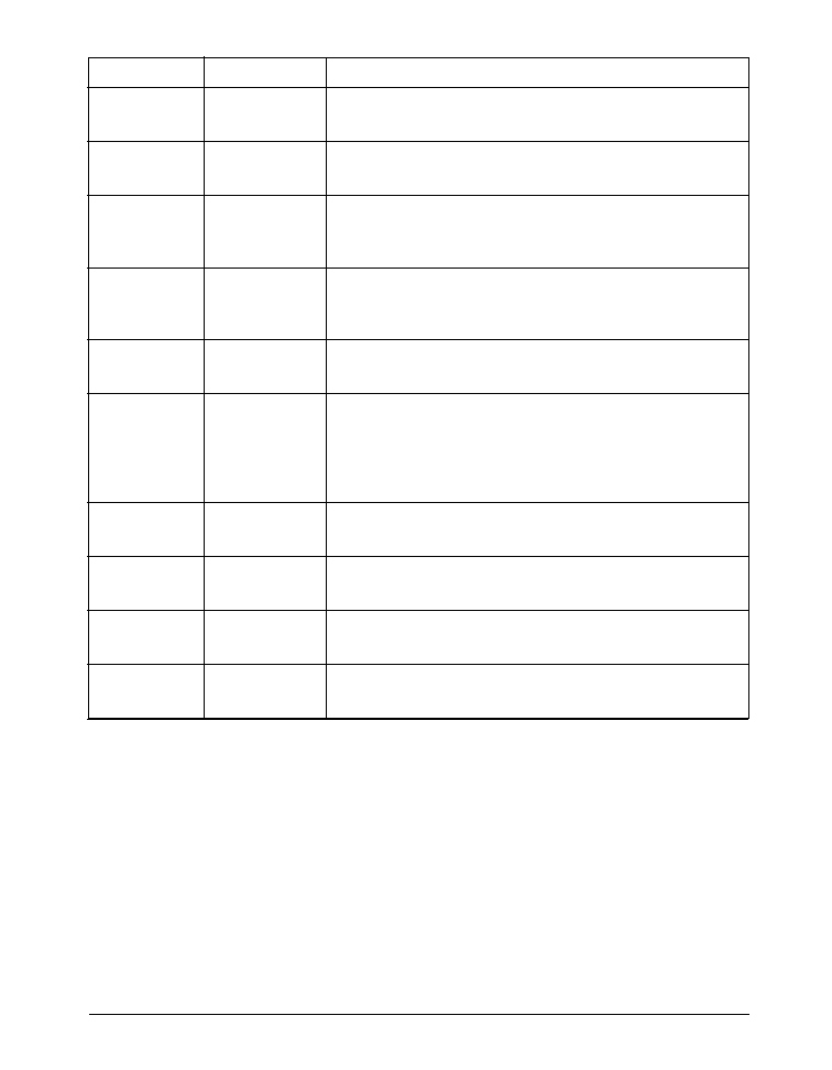
BOARD SCHEMATIC AND LAYOUT
The SP6650 Evaluation Board has been designed for easy and convenient access to all Inputs
and Outputs of the SP6650 device under test. Position the board with the silkscreen lettering
upright, (also see the drawing on the front page of this manual) and you will see the SP6650
MSOP, labeled U1 in the center of the board, and surrounding it the capacitors C
IN
, CV
IN
, CF, C
OUT
and resistors forming the switched DC-DC Converter circuit.
Rev. 3/23/01
SP6650 Evaluation Board Manual
© Copyright 2001 Sipex Corporation
2
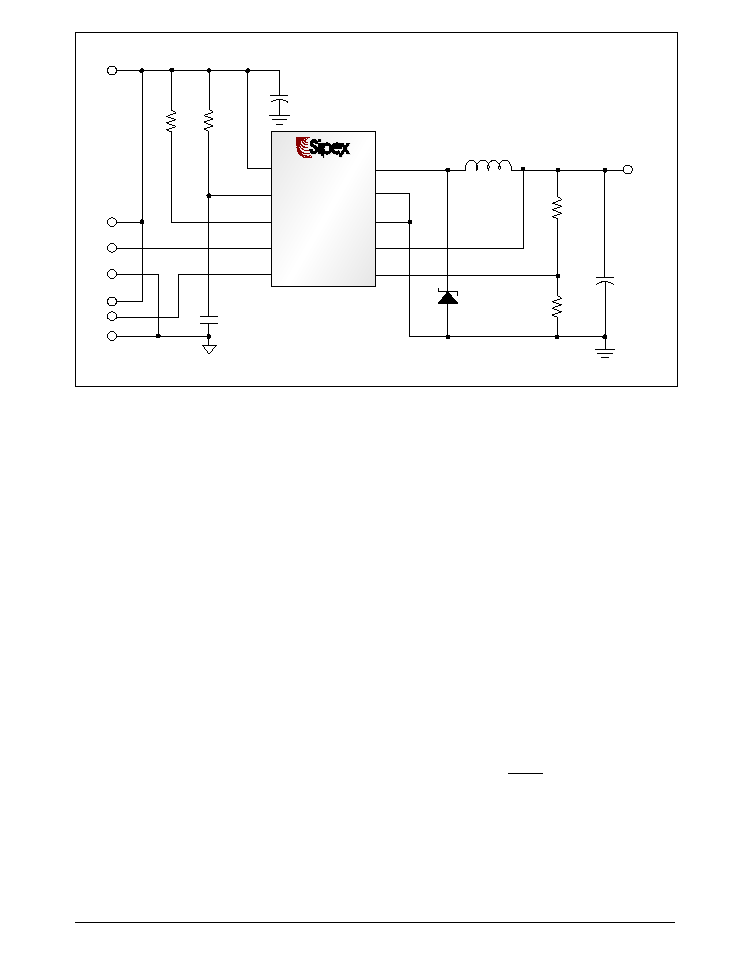
RB
100k
V
IN
2.7-6.5 VDC
SP6650
10
9
8
7
6
1
2
3
4
5
RV
IN
10.0
CV
IN
1.0
µ
F
L1 22
µ
H
V
OUT
3.3V
C
OUT
47
µ
F
RF
OPEN
R1
100k
PV
IN
V
IN
BLON
I
LIM
SHDN
LX
PGND
GND
V
OUT
FB
C
IN
47
µ
F
3
2
1
3
2
1
Æ
Æ
D1*
MBR0540TI
Figure 1. SP6650 Evaluation Board Schematic
The SP6650 Evaluation Board provides conve-
nient test points to connect the input to Power
Supply or Li-Ion Battery. The Input and Output
connections are made with raised female pin
receptacles which can accommodate easy-hook
connection leads for power and meter connec-
tions, as well as scope probe hooks and grounds
for waveform measurements.
USING THE EVALUATION BOARD
1) Powering Up the SP6650 Circuit
The SP6650 Evaluation Board can be powered
from a single Li-Ion battery or a +2.7 to +6.5V
power supply. Connect with short leads directly
to the "V
IN
" and "GND" posts. Note the SP6650
will remain in "shutdown" until pin 2 of the
Jumper J2 is applied to the GND.
2) I LIM Programming
Connect pin 4 of the SP6650 to V
IN
for 0.8 A
peak Inductor current limit (pins 2,3 of the
Jumper J2).
Connect pin 4 of the SP6650 to GND for 0.35
A peak Inductor current limit (pins 1,2 of the
Jumper J2).
3) V
OUT
Programming
To control the output voltage externally con-
nect the appropriate resistors (Table 1)
From pin 6 SP6650 FB to V
OUT
and to the
GND.
Tie Pin 6 FB to the 100k resistor or to the
GND and controller will use the internal
network for a preset output Voltage of 3.3V.
For V
OUT
different from shown in the Table
1, use equation:
RF =
(
V
OUT
≠ 1
)
R1
1.25
(For V
OUT
> 3.3V, RF = 50k recommended)
Rev. 3/23/01
SP6650 Evaluation Board Manual
© Copyright 2001 Sipex Corporation
3
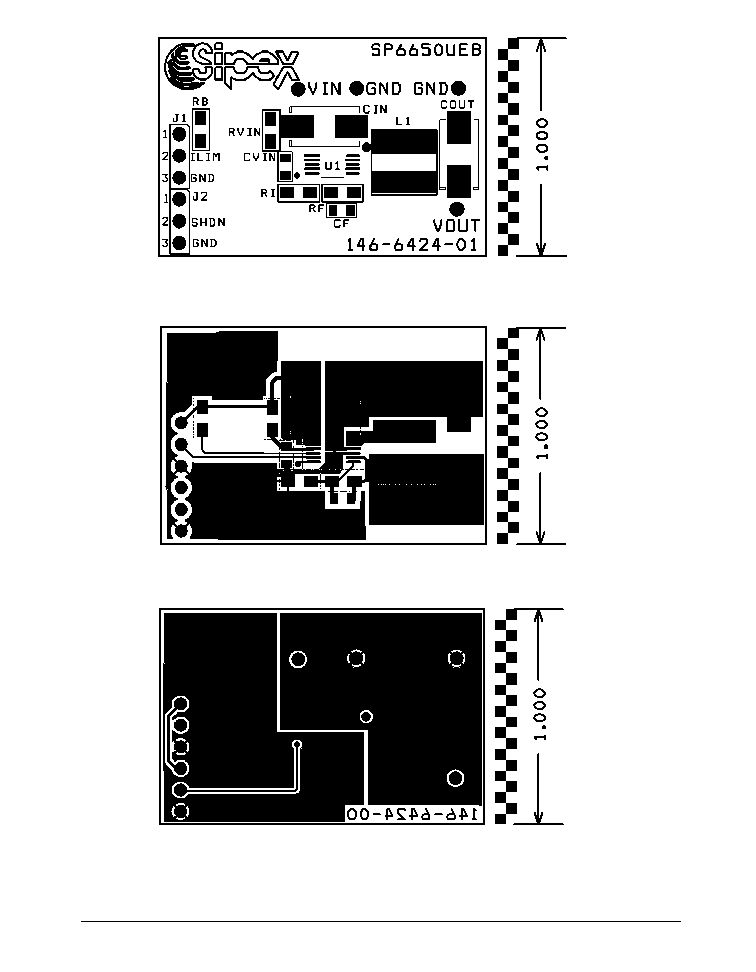
Figure 3: SP6650UEB PC layout Top Side
Figure 4: SP6650UEB PC Layout Bottom Side
Figure 2: SP6650UEB Component Placement
Rev. 3/23/01
SP6650 Evaluation Board Manual
© Copyright 2001 Sipex Corporation
4
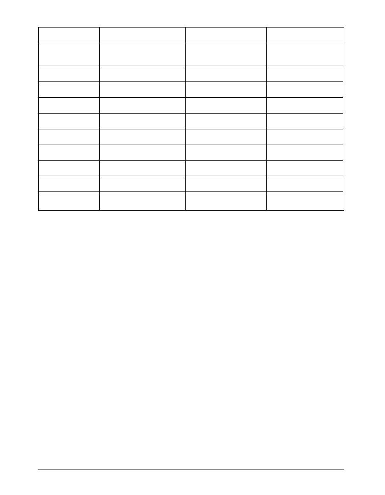
TABLE 1: SP6650UEB LIST OF MATERIALS
Component
V
OUT
= 3.3V, Int FB
V
OUT
= 2.5V, Ext FB
V
OUT
= 1.25V, Ext FB
L1
22
µ
H,CDRH6D28
22
µ
H,CDRH6D28
22
µ
H,CDRH6D28
Sumida
Sumida
Sumida
C
IN
47
µ
F, AVX TPSD
47
µ
F, AVX TPSD
47
µ
F, AVX TPSD
C
OUT
47
µ
F, AVX TPSD
47
µ
F, AVX TPSD
47
µ
F, AVX TPSD
RB
100k 5%
100k 5%
100k 5%
RV
IN
10
5%
10
5%
10
5%
CV
IN
1
µ
F ceramic
1
µ
F ceramic
1
µ
F ceramic
RI
100k 1%
100k 1%
100k 1%
RF
open
100k 1%
short
CF
open
470pF ceramic
open
U1
SP6650
SP6650
SP6650
Rev. 3/23/01
SP6650 Evaluation Board Manual
© Copyright 2001 Sipex Corporation
5
PIN DESCRIPTION
PIN NUMBER
PIN NAME
DESCRIPTION
1
PV
IN
Input voltage power pin. Inductor charging current passes
through this pin.
2
V
IN
Internal supply voltage. Control circuitry powered from this
pin.
3
BLON
Open drain battery low output. V
IN
below battery low thresh-
old pulls this node to ground. V
IN
above threshold, this node
is open.
4
I
LIM
Inductor current limit programming pin. Tie pin to V
IN
for 0.8A
peak inductor current limit. Tie pin to ground for 0.4A peak
inductor current limit. TTL input threshold.
5
SHDN
Shutdown control input. Tie to V
IN
for normal operation, tie to
ground for shutdown. TTL input threshold.
6
FB
External feedback network input connection. Connect a
resistor from FB to ground and FB to V
OUT
to control the
output voltage externally. This pin regulates to the internal
bandgap reference voltage of 1.25V. Tie FB to ground to use
the internal divider for a preset output voltage of 3.3V.
7
V
OUT
Output voltage sense pin. Used for internal feedback divider
and timing circuit.
8
GND
Internal ground pin. Control circuitry returns current to this
pin.
9
PGND
Power ground pin. Synchronous rectifier current returns
through this pin.
10
LX
Inductor switching node. Inductor tied between this pin and
the output capacitor to create regulated output voltage.
Rev. 3/23/01
SP6650 Evaluation Board Manual
© Copyright 2001 Sipex Corporation
6
ORDERING INFORMATION
Corporation
SIGNAL PROCESSING EXCELLENCE
Sipex Corporation reserves the right to make changes to any products described herein. Sipex does not assume any liability arising out of the
application or use of any product or circuit described herein; neither does it convey any license under its patent rights nor the rights of others.
Sipex Corporation
Headquarters and
Sales Office
22 Linnell Circle
Billerica, MA 01821
TEL: (978) 667-8700
FAX: (978) 670-9001
e-mail: sales@sipex.com
Sales Office
233 South Hillview Drive
Milpitas, CA 95035
TEL: (408) 934-7500
FAX: (408) 935-7600
Part Number
Temperature Range
Package
SP6650UEB .............................................................................................................. SP6650 Evaluation Board
SP6650EU ........................................................... -40
∞
C to +85
∞
C ............................................... 10-pin MSOP