 | –≠–ª–µ–∫—Ç—Ä–æ–Ω–Ω—ã–π –∫–æ–º–ø–æ–Ω–µ–Ω—Ç: SP6659 | –°–∫–∞—á–∞—Ç—å:  PDF PDF  ZIP ZIP |

1
Date: 07/20/05 SP6659 1.5MHz, 600mA Synchronous Buck Regulator © Copyright 2005 Sipex Corporation
SP6659
The SP6659 is a 600mA synchronous buck regulator using a constant frequency, current mode
architecture. The output voltage can be programmed using an external resistor divider. The 2.5V
to 5.5V input voltage range is ideal for portable applications that use a Li-Ion battery. Switching
frequency is internally set at 1.5MHz, allowing the use of small surface mount inductors and
capacitors. The internal synchronous switch increases efficiency and eliminates the need for an
external Schottky diode. The output voltage can be programmed using an external resistor
divider. Low output voltages are easily supported with the 0.6V feedback reference voltage. The
SP6659 is available in a low profile 5 pin TSOT-23 package.
Æ
DESCRIPTION
FEATURES
94% Efficiency Possible
600mA Output Current at V
IN
= 3V
2.5V to 5.5V Input Voltage Range
1.5MHz constant frequency operation
No Schottky Diode Required
Output Voltages as low as 0.6V
Slope Compensated Current Mode
Operation for Excellent Line and Load
Transient Response
100 % Duty Cycle in LDO Mode
<1
µ
A Shutdown Current, Quiescent
Current of 300
µ
A
Over-temperature protected
Offered in Low Profile TSOT-23
package
APPLICATIONS
Cell Phones
Wireless and DSL Modems
DSC's
Portable Instruments
TYPICAL APPLICATION SCHEMATICS
Now Available in Lead Free Packaging
1.5MHz, 600mA Synchronous Buck Regulator
Preliminary
Æ
SP6659
4.7
µ
F
Ceramic
V
IN
GND
V
OUT
10
µ
F
Ceramic
V
FB
SW
2.2
µ
H
R1
R2
RUN
C2
22pF
1
4
3
5
2
5
4
SP6659
5 Pin TSOT-23
VIN
GND
RUN
SW
VFB
1
2
3
5
4
SP6659
5 Pin TSOT-23
VIN
GND
RUN
SW
VOUT
1
2
3
Adjustable
Fixed
Æ
SP6659
4.7
µ
F
Ceramic
V
IN
GND
V
OUT
10
µ
F
Ceramic
V
OUT
SW
2.2
µ
H
RUN
1
4
3
5
2
Adjustable
Fixed
2
Date: 07/20/05 SP6659 1.5MHz, 600mA Synchronous Buck Regulator © Copyright 2005 Sipex Corporation
PIN DESCRIPTION
Input Supply Voltage ......................................................... -0.3V to +6V
RUN, V
FB
Voltages .................................................. -0.3V to (V
IN
+ 0.3V)
SW Voltage ............................................................ -0.3V to (V
IN
+ 0.3V)
P-Channel Switch Source Current ............................................. 800mA
N-Channel Switch Sink Current .................................................. 800mA
Peak Switch Sink and Source Current ........................................... 1.3A
Operating Temperature ................................................. -40
∞
C to +85
∞
C
Storage Temperature ................................................. -65
∞
C to +150
∞
C
Junction Temperature (Note 1) .................................................. 125
∞
C
ABSOLUTE MAXIMUM RATINGS
These are stress ratings only and functional operation of the device at
these ratings or any other above those indicated in the operation sections
of the specifications below is not implied. Exposure to absolute maximum
rating conditions for extended periods of time may affect reliability.
ELECTRICAL CHARACTERISTICS
Note 1: Junction Temperature T
J
is calculated from the ambient temperature TA and ower dissipation P
D
according to the following formula: T
J
= T
A
+ P
D
X 220
∞
C/W
PIN #
PIN NAME
DESCRIPTION
1
RUN
Power down control pin. Forcing this pin above 1.5V enables the device. Forcing this
pin below 0.3V shuts down the device.
2
GND
Ground pin.
3
SW
Switching node.
4
V
IN
Power supply pin
5
V
FB
/ V
OUT
Adjustable Version: V
FB,
Feedback Input Pin. Connect FB to the center point of the
external resistor divider. The feedback threshold voltage is 0.6V.
Fixed Output Version: V
OUT,
Output Voltage Feedback Pin. An internal resistive
divider drops the output voltage down for comparison to the internal reference voltage.
Vin=Vrun=3.6V, Io=0mA, Tamb= -40∫C to +85∫C, typical values at 25∫C unless otherwise noted.
Parameter
Min
Typ
Max
Units
Conditions
Input Voltage Range
2.5
5.5
V
Input DC Supply Current
Active Mode
300
400
µA
Vfb = 0.5V, Vin = Vrun
Shutdown Mode
0.1
1
µA
Vin = 3.6V, Vrun = ZeroV
0.5880
0.6000
0.6120
Ta=+25∫C
0.5865
0.6000
0.6135
V
0∫C<Ta<+85∫C
0.5820
0.6000
0.6180
-40∫C < Ta < +85∫C
Vfb Input Bias Current
85
300
nA
Vfb = 1.0V
Vfb Line Regulation
-1
0.4
1
%/V
Vin = 2.5V to 5.5V
Vfb Load Regulation
-0.1
0.01
0.1
%/mA
ILoad = 0mA to 600mA
Regulated Output Voltage
1.455
1.500
1.545
V
SP6659EK1-1.5, -40∫C < Ta < +85∫C
1.746
1.800
1.854
V
SP6659EK1-1.8, -40∫C < Ta < +85∫C
Minimum Output Voltage
0.6
V
Peak inductor current
0.7
1.15
1.5
A
Vfb = 0.5V
Oscillator frequency
0.8
1.4
1.8
mHz
Closed Loop, ILoad=100mA
P-channel ON resistance
0.4
0.6
I
SW
= 100mA
N-channel ON resistance
0.4
0.6
I
SW
= -100mA
Vrun=ZeroV, Vin = 3.6V
Vsw=ZeroV, Vsw = Vin
Run Threshold Voltage
0.2
1
1.3
V
Run Leakage Current
±0.01
±1.5
µA
±1.0
µA
Vfb (Feedback Voltage)
SW Leakage Current
±0.01
3
Date: 07/20/05 SP6659 1.5MHz, 600mA Synchronous Buck Regulator © Copyright 2005 Sipex Corporation
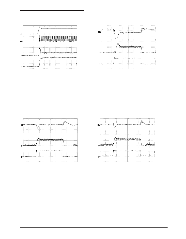
Figure 2: Load Transient 0mA to 600mA
Figure 3: Load Transient 50mA to 650mA
Figure 4: Load Transient 100mA to 700mA
TYPICAL PERFORMANCE CHARACTERISTICS
Refer to the typical application schematic, T
AMB
= +27
∞C
Figure 1: Fast V
IN
Startup (Scope: 50
µ
s/div)
CH 1: Switch Node, 5V/ div
CH 2: Inductor Current, 1A/ div
CH 3:
V
OUT,
1V/ div
CH 4:
V
IN,
5V/ div
CH 1: Output Voltage, 100mV per division AC-
Coupled
CH 2: Load Current, 500mA/ div
CH 3:
Inductor Current
, 500mA/ div
CH 1: Output Voltage, 100mV per division AC-
Coupled
CH 2: Load Current, 500mA/ div
CH 3:
Inductor Current
, 500mA/ div
CH 1: Output Voltage, 100mV per division AC-
Coupled
CH 2: Load Current, 500mA/ div
CH 3:
Inductor Current
, 500mA/ div
4
Date: 07/20/05 SP6659 1.5MHz, 600mA Synchronous Buck Regulator © Copyright 2005 Sipex Corporation
TYPICAL PERFORMANCE CHARACTERISTICS
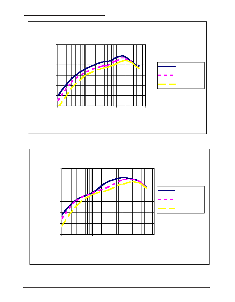
SP6659 Efficiency vs. Load Current
V
OUT
= 1.2V
40
50
60
70
80
90
100
1
10
100
1000
Load Current (mA)
Efficiency (%)
Vin = 2.7V
Vin = 3.3V
Vin = 4.2V
SP6659 Efficiency vs. Load Current
V
OUT
= 1.8V
40
50
60
70
80
90
100
1
10
100
1000
Load Current (mA)
Efficiency (%)
Vin = 2.7V
Vin = 3.3V
Vin = 4.2V
Figure 5: Efficiency Vs. Load Current, Vout =1.2V
Figure 6: Efficiency Vs. Load Current, Vout =1.8V
5
Date: 07/20/05 SP6659 1.5MHz, 600mA Synchronous Buck Regulator © Copyright 2005 Sipex Corporation
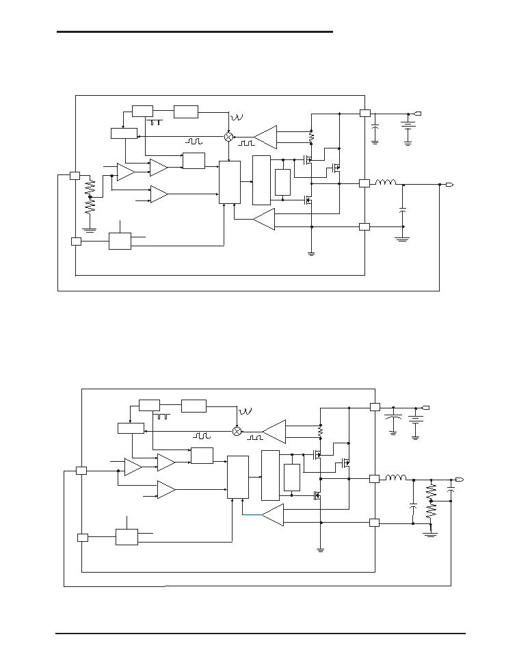
FUNCTIONAL DIAGRAMS
Q
R
Q
S
V
IN
2.7 - 5.5V
C
OUT
_
+
-
+
-
DRV
REF
0.6V
BLANKING
OSC
SLOPE
+
-
PWM
LOGIC
COMP
+
-
R
+
-
2
3
5
EA
OV
DET
COMP
0.65V
V
IN
SHUTDOWN
0.6V
_
_
Izero
COMP
NON-
OVERLAP
CONTROL
I
SENSE
COMP
RS LATCH
4
1
+
-
R2
SW
GND
R1
V
OUT
V
FB
RUN
C
2
C
IN
Adjustable Output Version
Fixed Output Version
Q
R
Q
S
V
IN
2.7 - 5.5V
C
OUT
_
+
-
+
-
DRV
REF
0.6V
BLANKING
OSC
SLOPE
+
-
PWM
LOGIC
COMP
+
-
R
+
-
2
3
5
EA
OV
DET
COMP
0.65V
V
IN
SHUTDOWN
0.6V
_
_
Izero
COMP
NON-
OVERLAP
CONTROL
I
SENSE
COMP
RS LATCH
4
1
+
-
SW
GND
V
OUT
V
OUT
RUN
R2
R1
C
IN