 | –≠–ª–µ–∫—Ç—Ä–æ–Ω–Ω—ã–π –∫–æ–º–ø–æ–Ω–µ–Ω—Ç: SP6681EU | –°–∫–∞—á–∞—Ç—å:  PDF PDF  ZIP ZIP |
1
Rev:A Date: 11/20/03
SP6681 High Efficiency Boost Charge Pump Regulator © Copyright 2002 Sipex Corporation
PRELIMINARY INFORMATION
High Efficiency Boost Charge Pump Regulator
SP6681
FEATURES
Ideal for Li Ion or 3V to 5V Conversion
Low Profile, Inductorless Regulator
Up To 96% Power Efficiency
+2.7V to +5.5V Input Voltage Range
5.0V, 50mA Output, 4% Accuracy
Low EMI Design
Low Quiescent Current: 175
µ
A
Low Shutdown Current:
4
µ
A
Optional External Clock: 32.768kHz
Thermal Shutdown Protection
Programmable Frequencies:
8.192kHz, 32.768kHz, or 262.14kHz
Internal Oscillator: 16kHz or 130kHz,
when CLK Pin Is Held High
Ultra small 10-Pin MSOP Package
DESCRIPTION
The SP6681 is a charge pump ideal for converting a +3.6V Li-Ion battery input to a +5.0V
regulated output. An input voltage range of +2.7V to +5.5V is converted to a regulated output
of 5.0V. The SP6681 device will operate at three different switching frequencies correspond-
ing to three different output resistances and load current ranges. An external 32.768kHz
nominal clock signal is used to produce three synchronized pump frequencies through the use
an internal phase lock loop to drive the charge pump. Two control inputs can adjust the internal
pump frequency on the fly to 8.192kHz (f
INPUT
/ 4), 32.768kHz (f
INPUT
x 1), or 262.14kHz (f
INPUT
x 8). The charge pump configuration dynamically changes to optimize power efficiency. At
low input voltages the charge pump doubles the input while at higher inputs the output is 1.5
times the input. The SP6681 can deliver high power efficiencies up to 96% with low quiescent
currents from 175
µ
A to 800
µ
A. The SP6681 is offered in a 10-Pin
µ
SOIC package.
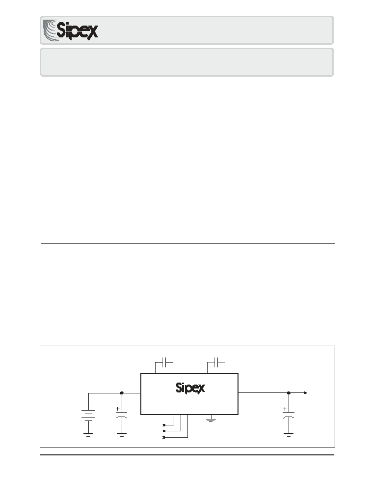
Æ
V
OUT
C/4
Cx8
CLK
GND
SP6681
8
CF1P
CF1N
CF2P
CF2N
4.7
µ
F
2.2
µ
F
2
9
10
7
1
6
4
5
3
+3.6V
Lithium-Ion
Battery
+5.0V output
V
IN
2.2
µ
F
2.2
µ
F
*All Capacitors Are Ceramic
APPLICATIONS
GSM SIM Card Power Supplies
3V to 5V Boost Applications
Li Ion to 5.0V Boost Applications
White LED Driver
Smart Card Readers
2
Rev:A Date: 11/20/03
SP6681 High Efficiency Boost Charge Pump Regulator © Copyright 2002 Sipex Corporation
PRELIMINARY INFORMATION
ABSOLUTE MAXIMUM RATINGS
These are stress ratings only and functional operation
of the device at these ratings or any other above those
indicated in the operation sections of the specifications
below is not implied. Exposure to absolute maximum
rating conditions for extended periods of time may
affect reliability.
V
IN
.........................................................-0.3V to +6.0V
V
OUT
......................................................-0.3V to +6.0V
I
OUT
....................................................................100mA
Storage Temperature........................-65∞C to +150∞C
Power Dissipation Per Package
10-pin mSOIC
(derate 8.84mW/
O
C above +70
O
C)..................720mW
Junction Temperature........................................125∞C
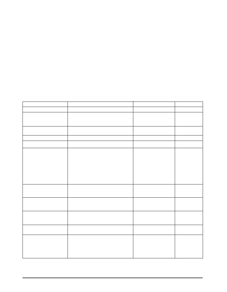
SPECIFICATIONS
V
IN
= +2.75 to +5.5V, f
CLK
= 32.768kHz, C
IN
= 4.7
µ
F (ceramic), CF1 = CF2 = C
OUT
= 2.2
µ
F, (ESR = 0.03
)
and T
AMB
= -40∞C to +85∞C unless otherwise
noted.
PARAMETER
CONDITIONS
MIN.
TYP.
MAX.
UNITS
Supply Voltage, V
IN
2.75
3.6
5.5
V
Quiescent Current, I
Q
f
PUMP
= f
CLK
/4
175
250
µA
f
CLK
=f
PUMP
230
300
f
PUMP
= f
CLK
/8
580
1500
In-Rush Current into V
IN
,
2.7V V
IN
5.5V, N
OTE
1
500
mA
IN
RUSH
Off Current, I
OFF
clock not present
8
15
µA
Input Clock Freq., f
CLK
Operational (supplied externally)
32.768
kHz
Pump Frequency, f
PUMP
f
CLK
C/4pin input Cx8pin input
no input
X
X
0
kHz
Present
Low
Low
32.768
Present
High
Low
8.192
Present
X
High
262.140
High
Low
Low
16
High
Low
High
130
High
High
Low
0
Input Threshold Voltage
Digital inputs = f
CLK
, f
CLK
/4, f
CLK
x 8
V
IL
0.4
V
V
IH
1.3
Input Current
Digital inputs = f
CLK
, f
CLK
/4, f
CLK
x 8
I
IN(low)
0.1
10
µA
I
IN(high)
1.0
10
Mode Transition Voltage,
X1.5 to X2, V
IN
falling
f
pump
= f
CLK
/4, I
LOAD
= 1mA
3.55
3.70
3.85
V
f
pump
, f
CLK
, I
LOAD
= 5mA
3.55
3.70
3.85
Hysteresis for Mode
V
IN
rising to V
IN
falling
50
mVpp
Transition Voltage
Transient Response:
Max. Transient Amplitude; t=5µs
I
LOAD
f
PUMP
100µA to 2mA 8.192kHz
1.5
%
2mA to 20mA
32.768kHz
1.5
20mA to 50mA 262.14kHz
1.5
3
Rev:A Date: 11/20/03
SP6681 High Efficiency Boost Charge Pump Regulator © Copyright 2002 Sipex Corporation
PRELIMINARY INFORMATION
PARAMETER
CONDITIONS
MIN.
TYP.
MAX.
UNITS
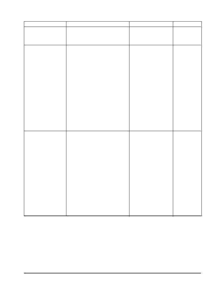
Output Resistance, R
OUT
Mode: X2, V
IN
=3.85V
I
LOAD
=2mA
f
PUMP
=8.192kHz
60
10mA
32.768kHz
20
50mA
262.14kHz
12.5
Average Output Voltage:
Ave V
OUT
f
PUMP
=8.192kHz; I
LOAD
=2mA
V
IN
Mode
3.0V
X2
4.8
5.0
5.2
V
3.55V
X2
4.8
5.0
5.2
3.85V
X1.5
4.8
5.0
5.2
3.5V
X1.5
4.8
5.0
5.2
f
PUMP
=32.768kHz; I
LOAD
=10mA
V
IN
Mode
3.0V
X2
4.8
5.0
5.2
V
3.55V
X2
4.8
5.0
5.2
3.85V
X1.5
4.8
5.0
5.2
3.5V
X1.5
4.8
5.0
5.2
f
PUMP
=262.14kHz; I
LOAD
=50mA
V
IN
Mode
3.0V
X2
4.8
5.0
5.2
V
3.55V
X2
4.8
5.0
5.2
3.85V
X1.5
4.8
5.0
5.2
3.5V
X1.5
4.8
5.0
5.2
Power Efficiency P
EFF
f
PUMP
=8.192kHz; I
LOAD
=2mA
V
IN
Mode
3.0V
X2
93
%
3.55V
X2
80
3.85V
X1.5
92
3.5V
X1.5
54
f
PUMP
=32.768kHz; I
LOAD
=10mA
V
IN
Mode
3.0V
X2
96
%
3.55V
X2
80
3.85V
X1.5
92
3.5V
X1.5
57
f
PUMP
=262.14kHz; I
LOAD
=50mA
V
IN
Mode
3.0V
X2
92
%
3.55V
X2
81
3.85V
X1.5
91
3.5V
X1.5
60
SPECIFICATIONS (CONT)
V
IN
= +2.75 to +5.5V, f
CLK
= 32.768kHz, C
IN
= 4.7
µ
F (ceramic), CF1 = CF2 = C
OUT
= 2.2
µ
F, (ESR = 0.03
)
and T
AMB
= -40∞C to +85∞C unless otherwise
noted.
NOTE 1: F
CLK
applied 10ms after V
IN
is present.
4
Rev:A Date: 11/20/03
SP6681 High Efficiency Boost Charge Pump Regulator © Copyright 2002 Sipex Corporation
PRELIMINARY INFORMATION
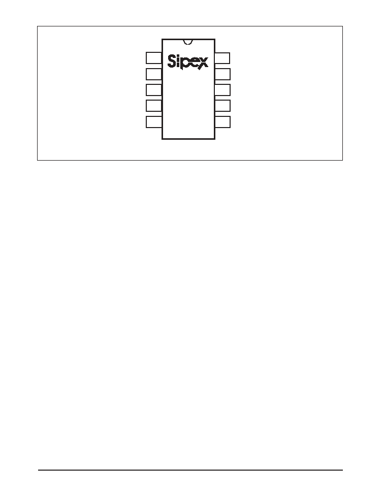
PIN ASSIGNMENTS
Pin 1-- V
OUT
-- 5.0V regulated charge pump.
Pin 2 -- CF1P -- Positive terminal to the charge
pump flying capacitor, CF1.
Pin 3 -- V
IN
-- Input pin for the +2.7V to +5.5V
supply voltage.
Pin 4 -- C/4 -- This is a control line for the
internal charge pump frequency. When this
control line is forced to a logic high, the
internal charge pump frequency is set to
1
/
4
of
the CLK frequency, provided that Cx8 is
low.
Pin 5 -- Cx8 -- This is a control line for the
internal charge pump frequency. When this
control line is forced to a logic high, the
internal charge pump frequency is set to x8 of
the CLK frequency.
Pin 6 -- CLK -- 32.768kHz Clock. Connect
this input pin to an external 32.768kHz clock
PINOUT
to drive the frequency of the charge pump.
Logic low inputs on the C/4 and Cx8 pins sets
the internal charge pump frequency accord-
ing to Table 1. Shutdown mode for the
device is set when there is no clock signal
present on this input pin, or when it is pulled
to ground.
Pin 7 -- CF2N -- Negative terminal to the
charge pump flying capacitor, CF2.
Pin 8 -- GND -- Ground reference.
Pin 9 -- CF2P -- Positive terminal to the charge
pump flying capacitor, CF2.
Pin 10 -- CF1N -- Negative terminal to the
charge pump flying capacitor, CF2.
C/4
V
IN
V
OUT
CLK
GND
SP6681
8
7
4
3
2
1
5
6
9
10
Cx8
CF1P
CF2P
CF1N
CF2N
5
Rev:A Date: 11/20/03
SP6681 High Efficiency Boost Charge Pump Regulator © Copyright 2002 Sipex Corporation
PRELIMINARY INFORMATION
DESCRIPTION
The SP6681 device is a regulated CMOS charge
pump voltage converter that can be used to
convert a +2.7V to +5.5V input voltage to a
nominal +5.0V output. These devices are ideal
for cellular phone designs involving battery-
powered and/or board level voltage conversion
applications.
An external clock signal with a frequency of
32.768kHz nominal is required for device
operation. A designer can set the SP6681 device
to operate at 3 different charge pump frequencies:
8.192kHz (f
INPUT
/ 4), 32.768kHz (f
INPUT
x 1), and
262.14kHz (f
INPUT
x 8). The three frequencies
correspond to three nominal load current ranges:
2mA, 20mA, and 50mA, respectively. The
SP6681 device optimizes for high power
efficiency with a low quiescent current of 175
µA
at 8.198kHz, 230
µA at 32.768kHz, and 800µA
at 262.14kHz. When there is no external clock
signal input, the device is in a low-power
shutdown mode drawing 4.4
µA (typical) current.
The SP6681 device is ideal for designs using
+3.6V lithium ion batteries such as cell phones,
PDAs, medical instruments, and other portable
equipment. For designs involving power sources
above +2.7V up to +5.5V, the internal charge
pump switch architecture dynamically selects an
operational mode that optimizes efficiency. The
SP6681 device regulates the maximum output
voltage to +5.0V.
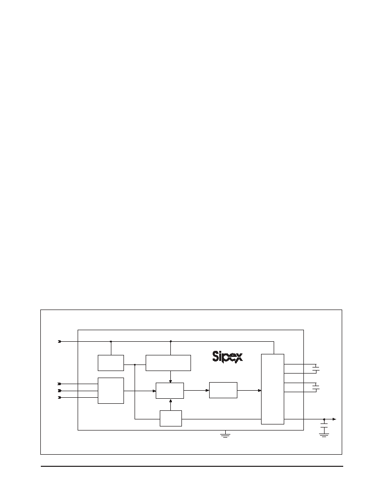
THEORY OF OPERATION
There are seven major circuit blocks for the
SP6681 device. Refer to Figure 1.
1) The Voltage Reference contains a band gap
and other circuits that provide the proper current
biases and voltage references used in the other
blocks.
2) The Clock Manager accepts the digital input
voltage levels (including the input clock) and
translates them to V
CC
and 0V. It also determines
if a clock is present in which case the device is
powered up. If the CLK input is left floating or
pulled near ground, the device shuts down and
V
IN
is shorted to V
OUT
. The worst case digital low
is 0.4V and the worst case digital high is 1.3V.
This block contains a synthesizer that generates
the internal pump clock which runs at the
frequency controlled with the C/4 and Cx8 logic
pins.
3) The Charge Pump Switch Configuration
Control determines the pump configuration
depending upon V
IN
as described earlier and
programs the Clock Phase Control. For an input
supply voltage from +2.7V to +3.7V, an X2
doubling architecture is enabled. This mode
requires one flying capacitor and one output
capacitor. For an input supply voltage greater
than +3.7V up to +5.5V, an X1.5 multiplier
architecture is enabled. This mode requires two
flying capacitors and one output capacitor.
Figure 1. Internal Block Diagram of the SP6681
V
OUT
Control
Voltage
Reference
CF1P
CF1N
CF2P
CF2N
CLK
C/4
Cx8
Clock
Manager
V
IN
G N D
SP6681
8
6
4
5
3
Charge Pump Switch
Configuration Control
Clock Phase
Reference
Drivers
Charge
Pump
Switches
V
OUT
CF1
CF2
C
OUT
6
Rev:A Date: 11/20/03
SP6681 High Efficiency Boost Charge Pump Regulator © Copyright 2002 Sipex Corporation
PRELIMINARY INFORMATION
4) The Clock Phase Control accepts the clock
and mode control generated by the Clock Manager
and the Charge Pump Switch Configuration
Control. This block then provides several clock
phases going to the Drivers block.
5) The V
OUT
Control regulates the Clock Phase
Control to ensure V
OUT
is regulated to 5.0V.
6) The Drivers block drives the clock phase
information to the gates of the large pump
transistors.
7) The Charge Pump Switch block contains the
large transistors that transfer charge to the fly
and load capacitors.
In normal operation of the device V
IN
is connected
between +2.7 and 5.5V. Refer to Figure 2 for a
typical application circuit. When no clock is
present (CLK is floating or near ground) the
device is in shutdown and the output is connected
to the input. This shutdown feature will work
either in start up or after the device is pumping.
Once a clock is present, the band gap is activated,
but only if V
IN
> 2.3V. Otherwise the device
remains in shutdown mode. Once the reference
voltage is stable, the device begins the pumping
operation.
If V
IN
< 3.70V, the device is configured as a
doubler. However, as the output reaches 5.0V,
the doubler action is truncated.
If V
IN
is above 3.70V, the device is reconfigured
and multiplies the input by a factor of 1.5. This
mode reduces the current drawn from the supply
and hence increases the power efficiency. As the
output reaches 5.0V, the charge transfer to the
load capacitor is truncated.
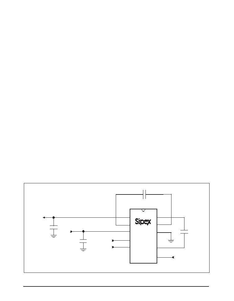
APPLICATION INFORMATION
Refer to Figure 3 for a typical SIM card
application circuit with the SP6681.
Oscillator Control
The external clock frequency required to drive
the internal charge pump oscillator is 32.768kHz
(nominal) at the CLK pin. When there is no
clock signal present at the CLK pin, the SP6681
device is in a low-power shutdown mode.
C/4 and Cx8 are two control lines for the internal
charge pump oscillator. When the C/4 control
line is forced to a logic high and the Cx8 control
line is at a low, the internal charge pump oscillator
is set to 8.192kHz. When both the C/4 and Cx8
control lines are at a logic low, the internal
charge pump oscillator is set to the input clock
signal, 32.768kHz. When the C/4 control line is
forced to a logic high, the internal charge pump
oscillator is set to 262.14kHz.
Figure 2. Typical Application for the SP6681
CF1P
V
IN
CF1N
GND
SP6681
5
3
2
1
4
C
IN
= 4.7
µ
F
C
OUT
= 2.2
µ
F
V
OUT
CF1 = 2.2
µ
F
C/4
Cx8
Frequency
Control
Inputs
CF2N
CF2P
CLK
10
9
8
7
6
CF2 = 2.2
µ
F
Input Clock
2.7V to 5.5V
5.0V
7
Rev:A Date: 11/20/03
SP6681 High Efficiency Boost Charge Pump Regulator © Copyright 2002 Sipex Corporation
PRELIMINARY INFORMATION
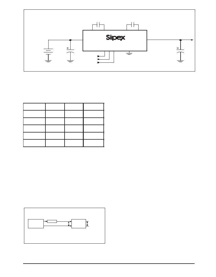
Figure 3. Typical SIM Card Application Circuit for the SP6681
Any standard CMOS logic output is suitable for
driving the C/4 or Cx8 control lines as long as
logic low is less than 0.4V and logic high is
greater than 1.3V.
Efficiency
Power efficiency with the SP6681 charge pump
regulator is improved over standard charge pumps
doubler circuits by the inclusion of an 1.5X
output mode, as described in the Theory of
Operation section. The net result is an increase
in efficiency at battery inputs greater than 3.7 to
3.8V where the SP6681 switches to the 1.5X
mode.
Figure 4. Capacitor Selection Test Circuit
n
i
p
K
L
C
n
i
p
4
/
C
n
i
p
8
x
C
f
P
M
U
P
t
n
e
s
e
r
p
t
o
n
X
X
0
z
H
k
8
6
7
.
2
3
w
o
l
w
o
l
z
H
k
8
6
7
.
2
3
z
H
k
8
6
7
.
2
3
w
o
l
h
g
i
h
z
H
k
4
1
.
2
6
2
z
H
k
8
6
7
.
2
3
h
g
i
h
w
o
l
z
H
k
2
9
1
.
8
z
H
k
8
6
7
.
2
3
h
g
i
h
h
g
i
h
z
H
k
4
1
.
2
6
2
Table 1. Control Line Logic for the Internal Charge
Pump Oscillator
V
OUT
C/4
Cx8
CLK
GND
SP6681
8
CF1P
CF1N
CF2P
CF2N
4.7
µ
F
2.2
µ
F
2
9
10
7
1
6
4
5
3
+3.6V
Lithium-Ion
Battery
V
IN
2.2
µ
F
2.2
µ
F
5.0V output
Power Supply
HP3631A
1000
µ
F
0.25ohm
0.75" Leads
+
-
V
IN
(p-p)
SP6681 EvBd
2.2
µ
F Caps
V
OUT
(p-p)
Capacitor Selection
In order to maintain the lowest output resistance,
input ripple voltage and output ripple voltage,
multi-layer ceramic capacitors with inherently
low ESR are recommended. Refer to Table 2 for
some suggested low ESR capacitors. Tables of
output resistance and ripple voltages for a vari-
ety of input, output and pump capacitors are
included here to use as a guide in capacitor
selection. Measured conditions are with CLK =
32kHz, 5mA output load and all capacitors are
2.2uF except when stated otherwise. A DC
power supply with added 0.25ohm output ESR
was used to simulate a Lithium Ion Battery as
shown in figure 4.
Board Layout
PC board layout is an important design consider-
ation to mitigate switching current effects. High
frequency operation makes PC layout important
for minimizing ground bounc and noise. Com-
ponents should be place as close to the IC as
possible with connections made through short,
low impedance traces. To maximize output
ripple voltage, use a ground plane and solder the
IC's GND pin directly to the ground plane.
8
Rev:A Date: 11/20/03
SP6681 High Efficiency Boost Charge Pump Regulator © Copyright 2002 Sipex Corporation
PRELIMINARY INFORMATION
#
E
N
O
H
P
E
L
E
T
/
R
E
R
U
T
C
A
F
U
N
A
M
R
E
B
M
U
N
T
R
A
P
/
E
C
N
A
T
I
C
A
P
A
C
E
G
A
T
L
O
V
R
S
E
X
A
M
z
H
k
0
0
1
@
R
O
T
I
C
A
P
A
C
E
P
Y
T
/
E
Z
I
S
0
0
1
6
-
3
0
8
-
7
4
8
/
K
D
T
K
5
2
2
A
1
R
5
X
2
1
0
2
C
2
.
2
µ
V
0
1
/
F
0
3
0
.
0
R
5
X
/
5
0
8
0
0
0
1
6
-
3
0
8
-
7
4
8
/
K
D
T
K
5
7
4
C
1
R
5
X
6
1
2
3
C
7
.
4
µ
V
0
1
/
F
0
2
0
.
0
R
5
X
/
6
0
2
1
1
1
4
9
-
8
4
4
-
3
4
8
/
X
V
A
K
5
2
2
C
Z
6
0
2
1
2
.
2
µ
V
0
1
/
F
0
3
0
.
0
R
7
X
/
6
0
2
1
8
8
8
0
-
5
2
9
-
7
4
8
/
n
e
d
u
Y
o
y
i
a
T
G
M
5
2
2
J
B
2
1
2
K
M
L
2
.
2
µ
V
0
1
/
F
0
3
0
.
0
R
5
X
/
5
0
8
0
8
8
8
0
-
5
2
9
-
7
4
8
/
n
e
d
u
Y
o
y
i
a
T
L
M
5
7
4
J
B
6
1
3
K
M
L
7
.
4
µ
V
0
1
/
F
0
2
0
.
0
R
7
X
/
6
0
2
1
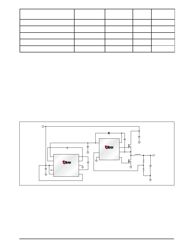
The SP6681 circuit shown in figure 5 acts as a
3.3V in to 5V out for biasing the two 5V Logic
Level N-channel MOSFETs used in a step-
down DC/DC converter. The high current
switching path is from the +3.3V bus through
the N-channel MOSFETs and inductor L1 to the
output capacitors. To fully enhance Logic-
Level N-channel MOSFETs, +5V is needed
from the SP6681 output to the SP6120 VCC pin,
which supplies the low-side MOSFET MN1
with a 0V to 5V gate pulse through the GL pin.
Table 2. Suggested Low ESR Cermic Surface Mount Capacitors.
For the top-side MOSFET MN2 (which has a
floating gate driver biased at the BST pin), the
boost pin BST is charge pumped up from the 0
to 3.3V switching at the switch node pin SWN,
with an additional 5V from SP6681 output,
through the DBST diode to a total of 8.3V when
the SWN is at 3.3V, or a total of 5V from gate to
source to fully enhance the MOSFET MN2. For
a more detailed schematic of a step-down DC/
DC converter, see the SP6120 datasheet.
Figure 5. SP6681 Circuit as a 3.3V to 5.0V Boost for 5V N-Channel MOSFETs in Buck DC/DC Converter Circuit.
SP6120
VCC
VFB
PGND
BST
GH
SWN
GL
MN2
CIN
1.9V
1A to 7A
VOUT
RF
COUT
RI
MN1
DBST
3.3V
VIN
L1
2.2µF
2.2µF
2.2µF
SP6681
VOUT
CF1P
VIN
CD4
Cx8
CF2P
CF1N
GND
CF2N
CLK
10
9
8
7
6
1
2
3
4
5
4.7µF
130kHz Internal Clock
+5VOUT
CBST
9
Rev:A Date: 11/20/03
SP6681 High Efficiency Boost Charge Pump Regulator © Copyright 2002 Sipex Corporation
PRELIMINARY INFORMATION
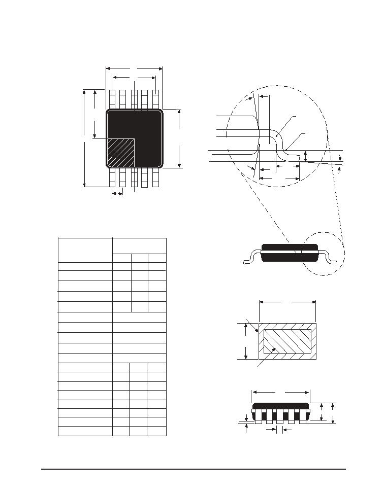
(ALL DIMENSIONS IN MILLIMETERS)
PACKAGE: 10-PIN MSOP
0.07 - -
L1
L
R1
ÿ
ÿ1
R
1
ÿ1
Seating Plane
1
E1
2
E/2
e1
e
E
D
Gauge Plane
L2
D
A2
A
A1
b
- - 1.1
0 - 0.15
Dimensions in (mm)
10-PIN MSOP
JEDEC MO-187
(BA) Variation
0.75 0.85 0.95
0.17 - 0.27
0.08 - 0.23
3.00 BSC
4.90 BSC
3.00 BSC
0.4 0.60 0.80
0.95
- 0.25 -
- 10 -
0.07 - -
0∫ 8∫
A
A1
A2
b
c
D
E
E1
L
L1
L2
N
R
R1
ÿ
0∫ - 15∫
ÿ1
MIN NOM MAX
e1
e
2.00 BSC
0.50 BSC
c
WITH PLATING
BASE METAL
(b)
-
-
Pin #1 indentifier must be indicated within this shaded area (D/2 * E1/2)
10
Rev:A Date: 11/20/03
SP6681 High Efficiency Boost Charge Pump Regulator © Copyright 2002 Sipex Corporation
PRELIMINARY INFORMATION
ORDERING INFORMATION
Model
Temperature Range
Package Type
SP6681EU .............................................. -40∞C to +85∞C ........................................ 10-pin
SOP
SP6681EU/TR ........................................ -40∞C to +85∞C ............... (tape and reel) 10-pin
SOP
SIGNAL PROCESSING EXCELLENCE
Sipex Corporation reserves the right to make changes to any products described herein. Sipex does not assume any liability arising out of the
application or use of any product or circuit described hereing; neither does it convey any license under its patent rights nor the rights of others.
Corporation
Sipex Corporation
Headquarters and
Sales Office
22 Linnell Circle
Billerica, MA 01821
TEL: (978) 667-8700
FAX: (978) 670-9001
e-mail: sales@sipex.com
Sales Office
233 South Hillview Drive
Milpitas, CA 95035
TEL: (408) 934-7500
FAX: (408) 935-7600