 | –≠–ª–µ–∫—Ç—Ä–æ–Ω–Ω—ã–π –∫–æ–º–ø–æ–Ω–µ–Ω—Ç: SP6691ER | –°–∫–∞—á–∞—Ç—å:  PDF PDF  ZIP ZIP |
1
Date: 01/26/05
SP6691 Micro Power Boost Regulator, Series White LED Driver © Copyright 2005 Sipex Corporation
SP6691
FEATURES
Drives up to 6 LED's @ 25mA
Drives up to 8 LED's @ 20mA
High Output Voltage: Up to 34V
Optimized for Single Supply,
2.7V - 4.2V Applications
Operates Down to 1V
High Efficiency: Greater Than 75%
Low Quiescent Current: 20µA
Ultra Low Shutdown Current: 10nA
Single Battery Cell Operation
Programmable Output Voltage
1 switch (350mV at 350mA)
Available in 8 Pin DFN, 5 Pin TSOT or
5 Pin SOT23
Micro Power Boost Regulator Series White LED Driver
APPLICATIONS
White LED Driver
High Voltage Bias
Digital Cameras
Cell Phone
Battery Backup
Handheld Computers
DESCRIPTION
The SP6691 is a micro power boost regulator that is specifically designed for powering series
configuration white LED. The part utilizes fixed off time architecture and consumes only 10nA
quiescent current in shutdown. Low voltage operation, down to 1V, fully utilizes maximal battery
life. The SP6691 is offered in a 8 Pin DFN, 5-pin SOT-23 or 5 Pin TSOT package and enables
the construction of a complete regulator occupying < 0.2 in
2
board space.
Æ
TYPICAL APPLICATION CIRCUIT
V
IN
SW
GND
SHDN
FB
10µH
2.2 µF
4.7µF
2.7 to 4.2V
Æ
R
b
SP6691
D1
L1
C1
C2
Now Available in Lead Free Packaging
NC
SHDN
V
IN
GND
NC
FB
NC
SW
8
7
6
5
1
2
3
4
SP6691
8 Pin DFN
2
Date: 01/26/05
SP6691 Micro Power Boost Regulator, Series White LED Driver © Copyright 2005 Sipex Corporation
V
IN
....................................................................... 15V
SW Voltage .............................................. -0.4 to 34V
FB Voltage ......................................................... 2.5V
All other pins ................................... -0.3 to V
IN
+ 0.3V
Current into FB ................................................. ±1mA
T
J
Max ............................................................. 125∞C
Operating Temperature Range ............ -40∞C to 85∞C
Peak Output Current < 10us SW .................... 500mA
Storage Temperature ...................... -65∞C to +150∞C
Power Dissipation. ......................................... 200mW
ESD Rating ................................................. 2kV HBM
These are stress ratings only and functional operation of the device at
these ratings or any other above those indicated in the operation sections
of the specifications below is not implied. Exposure to absolute maximum
rating conditions for extended periods of time may affect reliability.
PIN DESCRIPTION
ELECTRICAL CHARACTERISTICS
ABSOLUTE MAXIMUM RATINGS
Specifications are at T
A
= 25∞C, V
IN
= 3.3, V
SHDN
= V
IN
,
denotes the specifications which apply over the full operating
temperature range, unless otherwise specified.
PIN NUMBER
PIN NAME
8 PIN DFN DESCRIPTION
1
NC
No connect.
2
FB
Feedback.
3
NC
No connect.
3
SW
Switch input to the internal power switch
5
GND
Ground
6
V
IN
Input Voltage. Bypass this pin with a capacitor as close to the device
as possible.
7
SHDN
Shutdown. Pull high (on) to enable. Pull low (off) for shutdown.
8
NC
No connect.
PARAMETER
SYMBOL
MIN
TYP
MAX
UNITS
CONDITIONS
Input Voltage
V
IN
1.0
13.5
V
Supply Current
I
Q
20
30
µA
No Switching
0.01
1
µA
SHDN = 0V (off)
Reference Voltage
V
FB
1.17
1.22
1.27
V
FB Hysteresis
HYST
8
mV
V
FB
Input Bias Current
I
FB
15
80
nA
V
FB
= 1.22V
Line Regulation
V
o
/V
I
0.1
0.3
%/V
1.2 V
IN
13.5V
Switch Off Time
T
OFF
250
nS
Switch Saturation Voltage
V
CESAT
170
450
mV
I
SW
= 325mA
Switch Current Limit
I
LIM
325
450
575
mA
SHDN Bias Current
I
SHDN
5
12
µA
V
SHDN
= 3.3V
SHDN High Threshold (on)
V
IH
0.9
V
SHDN Low Threshold (off)
V
IL
0.25
V
Switch Leakage Current
I
SWLK
0.01
5
µA
Switch Off, V
SW
= 5V
3
Date: 01/26/05
SP6691 Micro Power Boost Regulator, Series White LED Driver © Copyright 2005 Sipex Corporation
+
-
4
Q1
Q2
R3
R4
R2
R1
X1
Shutdown
Logic
250ns
ONE-SHOT
CLEAR
X2
+
-
SET
DRIVER
GND
2
1
5
3
SW
POWER
TRANSISTOR
DISABLE
VIN
SHDN
FB
FUNCTIONAL DIAGRAM
THEORY OF OPERATION
Operation can be best understood by referring to
the functional diagram above and the typical
application circuit in the front page. Q1 and Q2
along with R3 and R4 form a band gap refer-
ence. The input to this circuit completes a feed-
back path from the high voltage output through
a voltage divider, and is used as the regulation
control input. When the voltage at the FB pin is
slightly above 1.22V, comparator X1 disables
most of the internal circuitry. Current is then
provided by capacitor C2, which slowly dis-
charges until the voltage at the FB pin drops
below the lower hysteresis point of X1, about
6mV. X1 then enables the internal circuitry,
turns on chip power, and the current in the
inductor begins to ramp up. When the current
through the driver transistor reaches about
450mA, comparator X2 clears the latch, which
turns off the driver transistor for a preset 250nS.
At the instant of shutoff, inductor current is
diverted to the output through diode D1. During
this 250nS time limit, inductor current decreases
while its energy charges C2.
At the end of the 250ns time period, driver
transistor is again allowed to turn on which
ramps the current back up to the 450mA level.
Comparator X2 clears the latch, it's output turns
off the driver transistor, and this allows delivery
of L1's stored kinetic energy to C2. This switch-
ing action continues until the output capacitor
voltage is charged to the point where FB is at
band gap (1.22V). When this condition is
reached, X1 turns off the internal circuitry and
the cycle repeats.
PIN DESCRIPTION
PIN NUMBER
PIN NAME
DESCRIPTION
1
SW
Switch input to the internal power switch.
2
GND
Ground
3
FB
Feedback
4
SHDN
Shutdown. Pull high (on) to enable. Pull low (off) for shutdown.
5
V
IN
Input Voltage. Bypass this pin with a capacitor as close to the device
as possible.
4
Date: 01/26/05
SP6691 Micro Power Boost Regulator, Series White LED Driver © Copyright 2005 Sipex Corporation
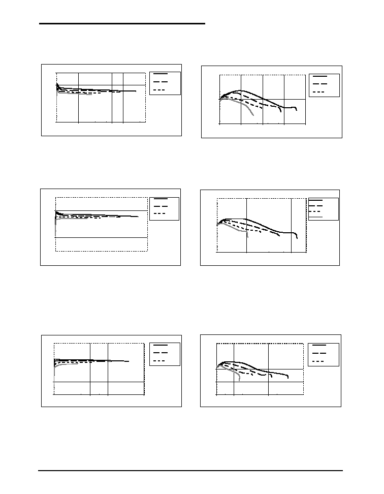
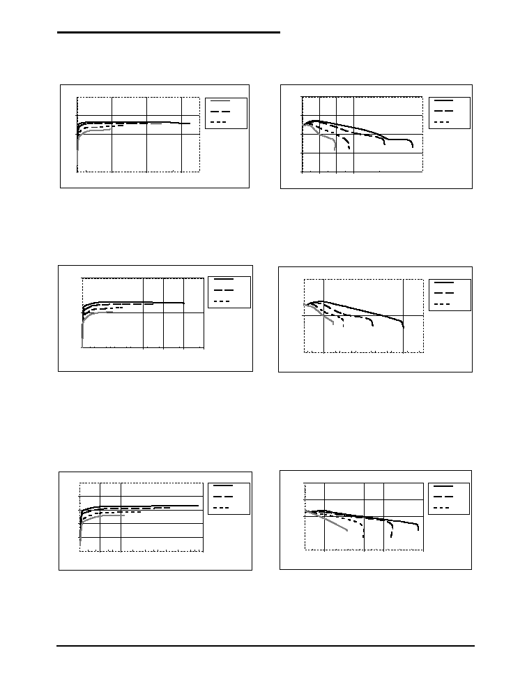
PERFORMANCE CHARACTERISTICS
Refer to the typical application circuit, T
AMB
= 25
∞C, unless otherwise specified.
Figure 1. 12V Output Efficiency
Figure 2. 12V Output Load Regulation
Figure 3. 15V Output Efficiency
Figure 4. 15V Output Load Regulation
Figure 5. 18V Output Efficiency
Figure 6. 18V Output Load Regulation
Vout = 12V Efficiency
50
60
70
80
90
0
20
40
60
80
100
120
140
160
Iout (mA)
Efficiency (%)
Vin =
5.0V
Vin =
4.2V
Vin =
3 3V
Vout = 12V Load Regulation
11.0
11.5
12.0
12.5
13.0
0
20
40
60
80
100
120
140
160
Iout (mA)
Vout (V)
Vin =
5.0V
Vin =
4.2V
Vin =
3 3V
Vout = 15V Efficiency
50
60
70
80
90
0
20
40
60
80
100
120
Iout (mA)
Efficiency (%)
Vin =
5.0V
Vin =
4.2V
Vin =
3.3V
Vi
Vout = 15V Load Regulation
14.0
14.5
15.0
15.5
16.0
0
20
40
60
80
100
120
Iout (mA)
Vout (V)
Vin = 5.0V
Vin = 4.2V
Vin = 3.3V
Vin = 2.7V
Vout = 18V Efficiency
50
60
70
80
90
0
20
40
60
80
100
Iout (mA)
Efficiency (%)
Vin =
5.0V
Vin =
4.2V
Vin =
3 3V
Vout = 18V Load Regulation
17.0
17.5
18.0
18.5
19.0
0
20
40
60
80
100
Iout (mA)
Vout (V)
Vin =
5.0V
Vin =
4.2V
Vin =
3 3V
5
Date: 01/26/05
SP6691 Micro Power Boost Regulator, Series White LED Driver © Copyright 2005 Sipex Corporation
PERFORMANCE CHARACTERISTICS
Refer to the typical application circuit, T
AMB
= 25
∞C, unless otherwise specified.
Figure 7. 21V Output Efficiency
Figure 8. 21V Output Load Regulation
Figure 9. 24V Output Efficiency
Figure 10. 24V Output Load Regulation
Figure 11. 30V Output Efficiency
Figure 12. 30V Output Load Regulation
Vout = 21V Efficiency
50
60
70
80
90
0
10
20
30
40
50
60
70
Iout (mA)
Efficiency (%)
Vin =
5.0V
Vin =
4.2V
Vin =
3 3V
Vout = 21V Load Regulation
20.0
20.5
21.0
21.5
22.0
0
10
20
30
40
50
60
70
Iout (mA)
Vout (V)
Vin =
5.0V
Vin =
4.2V
Vin =
3 3V
Vout = 24V Efficiency
50
60
70
80
90
0
10
20
30
40
50
60
Iout (mA)
Efficiency (%)
Vin =
5.0V
Vin =
4.2V
Vin =
3 3V
Vout = 24V Load Regulation
23.0
23.5
24.0
24.5
25.0
0
10
20
30
40
50
60
Iout (mA)
Vout (V)
Vin =
5.0V
Vin =
4.2V
Vin =
3 3V
Vout = 30V Efficiency
40
50
60
70
80
90
0
5
10
15
20
25
30
Iout (mA)
Efficiency (%)
Vin =
5.0V
Vin =
4.2V
Vin =
3 3V
Vout = 30V Load Regulation
29.0
29.5
30.0
30.5
31.0
0
5
10
15
20
25
30
Iout (mA)
Vout (V)
Vin =
5.0V
Vin =
4.2V
Vin =
3 3V