1
SP6828DS/11 SP6828/6829 +3V Low Power Voltage Inverter © Copyright 2000 Sipex Corporation
s
99.9% Voltage Conversion Efficiency
s
+1.15V to +4.2V Input Voltage Range
s
+1.15 V
IN
Guaranteed Start-up
s
Inverts Input Supply Voltage
s
20
µ
A Quiescent Current for the SP6828
s
40
µ
A Quiescent Current for the SP6829
s
25mA Output Current
s
12kHz Operating Frequency for the SP6828
s
35kHz Operating Frequency for the SP6829
s
Ideal for +3.6V Lithium Ion Battery
Applications
s
Reverse +3.6V Lithium Ion Battery
Protection
s
5-pin SOT23 Package
+3V Low Power Voltage Inverters
SP6828/6829
DESCRIPTION
The SP6828/6829 devices are CMOS Charge Pump Voltage Inverters that can be
implemented in designs requiring a negative voltage from a +3V battery source. The SP6828/
6829 devices are ideal for both battery-powered and board level voltage conversion
applications with a typical operating current of 20
µ
A for the SP6828 and 40
µ
A for the SP6829.
Both devices can output 25mA with a voltage drop of 500mV. These devices combine a low
quiescent current with high efficiency (>95% over most of its load-current range), which is ideal
for designs using +3.3V or +3.6V lithium ion batteries. Applications include cell phones, PDAs,
medical instruments and other portable equipment. The SP6828/6829 devices are available in
a space-saving 5-pin SOT23 Package.
C1-
V
OUT
V
IN
C1+
GND
SP6828
SP6829
5
3
2
1
4
Æ
2
SP6828DS/11 SP6828/6829 +3V Low Power Voltage Inverter © Copyright 2000 Sipex Corporation
SPECIFICATIONS FOR THE SP6828/6829
V
IN
= +3.3V, C1=C2=10
µ
F for the SP6828, C1=C2=3.3
µ
F for the SP6829, and T
AMB
= -40
∞
C to +85
∞
C unless otherwise noted. Typical values are taken
specifically at T
AMB
=+25
∞
C. Test Circuit
Figure 19 unless otherwise noted.
NOTE 1: V
OUT
= -V
IN
+200mV
NOTE 2: Power Efficiency (Ideal) =
V
OUT
x I
OUT
-V
IN
x (-V
IN
/R
L
)
NOTE 3: Power Efficiency (Actual) =
V
OUT
x I
OUT
V
IN
x I
IN
ABSOLUTE MAXIMUM RATINGS
These are stress ratings only and functional operation of the device at
these ratings or any other above those indicated in the operation sections
of the specifications below is not implied. Exposure to absolute maximum
rating conditions for extended periods of time may affect reliability.
V
IN
...................................................................................................+4.5V
V
OUT
.................................................................................................-4.5V
V
OUT
Short Circuit to GND.................................................Indefinite
I
OUT
...................................................................................................50mA
Storage Temperature.....................................................-65∞C to +150∞C
Power Dissipation (T
AMB
=+70
∞
C).................................................571mW
Lead Temperature (Soldering)....................................................300
o
C
ESD Rating...............................................2kV Human Body Model
R
E
T
E
M
A
R
A
P
.
N
I
M
.
P
Y
T
.
X
A
M
S
T
I
N
U
S
N
O
I
T
I
D
N
O
C
e
g
a
t
l
o
V
y
l
p
p
u
S
5
1
.
1
4
.
1
6
8
.
0
2
.
4
V
R
L
k
0
1
=
T
,
B
M
A
1
e
t
o
N
,
C
∞
5
2
+
=
R
L
k
0
1
=
T
,
B
M
A
C
∞
5
8
+
o
t
C
∞
0
4
-
=
t
n
e
r
r
u
C
y
l
p
p
u
S
0
2
0
4
0
4
0
6
0
8
0
2
1
µ
A
8
2
8
6
P
S
T
,
B
M
A
R
,
C
∞
5
2
+
=
L
=
8
2
8
6
P
S
T
,
B
M
A
,
C
∞
5
8
+
o
t
C
∞
0
4
-
=
R
L
=
9
2
8
6
P
S
T
,
B
M
A
R
,
C
∞
5
2
+
=
L
=
9
2
8
6
P
S
T
,
B
M
A
,
C
∞
5
8
+
o
t
C
∞
0
4
-
=
R
L
=
e
c
n
a
t
s
i
s
e
R
t
u
p
t
u
O
9
2
0
5
5
6
I
T
U
O
T
,
A
m
5
=
B
M
A
C
∞
5
2
+
=
I
T
U
O
T
,
A
m
5
=
B
M
A
C
∞
5
8
+
o
t
C
∞
0
4
-
=
y
c
n
e
u
q
e
r
F
r
o
t
a
ll
i
c
s
O
4
.
8
7
5
.
4
2
0
2
2
1
5
3
6
.
5
1
8
1
5
.
5
4
3
5
z
H
k
8
2
8
6
P
S
T
,
B
M
A
C
∞
5
2
+
=
8
2
8
6
P
S
T
,
B
M
A
C
∞
5
8
+
o
t
C
∞
0
4
-
=
9
2
8
6
P
S
T
,
B
M
A
C
∞
5
2
+
=
9
2
8
6
P
S
T
,
B
M
A
C
∞
5
8
+
o
t
C
∞
0
4
-
=
y
c
n
e
i
c
i
f
f
E
n
o
i
s
r
e
v
n
o
C
e
g
a
t
l
o
V
5
9
9
.
9
9
%
R
L
=
)
l
a
e
d
I
(
y
c
n
e
i
c
i
f
f
E
r
e
w
o
P
7
9
%
R
L
k
0
1
=
2
E
T
O
N
,
)
l
a
u
t
c
A
(
y
c
n
e
i
c
i
f
f
E
r
e
w
o
P
5
9
1
9
%
R
L
k
0
1
=
3
E
T
O
N
,
I
T
U
O
3
E
T
O
N
,
A
m
0
1
=
3
SP6828DS/11 SP6828/6829 +3V Low Power Voltage Inverter © Copyright 2000 Sipex Corporation
R
E
T
E
M
A
R
A
P
.
N
I
M
.
P
Y
T
.
X
A
M
S
T
I
N
U
S
N
O
I
T
I
D
N
O
C
e
g
a
t
l
o
V
y
l
p
p
u
S
5
2
.
1
5
.
1
6
8
.
0
5
.
5
V
R
L
k
0
1
=
T
,
B
M
A
1
e
t
o
N
,
C
∞
5
2
+
=
R
L
k
0
1
=
T
,
B
M
A
C
∞
5
8
+
o
t
C
∞
0
4
-
=
t
n
e
r
r
u
C
y
l
p
p
u
S
0
5
5
1
1
µ
A
T
B
M
A
R
,
C
∞
5
8
+
o
t
C
∞
0
4
-
=
L
=
e
c
n
a
t
s
i
s
e
R
t
u
p
t
u
O
4
2
0
5
5
6
I
T
U
O
T
,
A
m
5
=
B
M
A
C
∞
5
2
+
=
I
T
U
O
T
,
A
m
5
=
B
M
A
C
∞
5
8
+
o
t
C
∞
0
4
-
=
y
c
n
e
u
q
e
r
F
r
o
t
a
ll
i
c
s
O
6
0
2
z
H
k
T
B
M
A
C
∞
5
8
+
o
t
C
∞
0
4
-
=
y
c
n
e
i
c
i
f
f
E
n
o
i
s
r
e
v
n
o
C
e
g
a
t
l
o
V
5
9
9
.
9
9
%
R
L
=
)
l
a
e
d
I
(
y
c
n
e
i
c
i
f
f
E
r
e
w
o
P
8
9
%
R
L
k
0
1
=
2
E
T
O
N
,
)
l
a
u
t
c
A
(
y
c
n
e
i
c
i
f
f
E
r
e
w
o
P
1
9
4
9
%
R
L
k
0
1
=
3
E
T
O
N
,
I
T
U
O
3
E
T
O
N
,
A
m
0
1
=
SPECIFICATIONS FOR THE SP6828-5
V
IN
= +5.0V, C1=C2=10
µ
F and T
AMB
= -40
∞
C to +85
∞
C unless otherwise noted.Typical values are taken specifically at T
AMB
=+25
∞
C.
Test Circuit
Figure 19 unless otherwise noted.
NOTE 1: V
OUT
= -V
IN
+200mV
NOTE 2: Power Efficiency (Ideal) =
V
OUT
x I
OUT
-V
IN
x (-V
IN
/R
L
)
NOTE 3: Power Efficiency (Actual) =
V
OUT
x I
OUT
V
IN
x I
IN
ABSOLUTE MAXIMUM RATINGS
These are stress ratings only and functional operation of the device at
these ratings or any other above those indicated in the operation sections
of the specifications below is not implied. Exposure to absolute maximum
rating conditions for extended periods of time may affect reliability.
V
IN
....................................................................................................+6.0V
V
OUT
.................................................................................................-6.0V
V
OUT
Short Circuit to GND.................................................Indefinite
I
OUT
...................................................................................................50mA
Storage Temperature.....................................................-65∞C to +150∞C
Power Dissipation (T
AMB
=+70
∞
C).........................................571mW
Lead Temperature (Soldering)......................................................300
o
C
ESD Rating..................................................2kV Human Body Model
4
SP6828DS/11 SP6828/6829 +3V Low Power Voltage Inverter © Copyright 2000 Sipex Corporation
PIN ASSIGNMENTS
Pin 1-- V
OUT
-- Inverting charge pump output.
Pin 2 -- V
IN
-- Input to the positive power
supply.
Pin 3 -- C1- -- Negative terminal to the charge
pump capacitor.
Pin 4 -- GND -- Ground reference.
Pin 5 -- C1+ -- Positive terminal to the charge
pump capacitor.
PINOUT
C1-
V
OUT
V
IN
C1+
GND
SP6828
SP6829
5
3
2
1
4
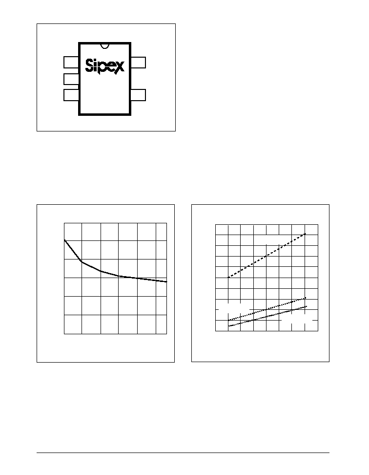
Figure 1. Output Resistance vs. Supply Voltage
Figure 2. Output Resistance vs. Temperature
TYPICAL PERFORMANCE CHARACTERISTICS
V
IN
= +3.3V, C1 = C2 = C3 = 10
µ
F for SP6828, C1 = C2 = C3 = 3.3
µ
F for SP6829, and T
AMB
= 25
o
C unless
otherwise noted. The SP6828/6829 devices use the circuit found in
Figure 19 when obtaining the following typical
performance characteristics (unless otherwise noted).
60
50
40
30
20
10
0
1.5 2.0
2.5
3.0
3.5
4.0
V
IN
(V)
R
OUT
(Ohm)
70
65
60
55
50
45
40
35
30
25
20
-60 -40 -20
0
20 40
Temperature (
o
C)
R
OUT
(Ohm)
60 80 100
V
IN
= 1.5V
V
IN
= 3.3V
V
IN
= 4.2V
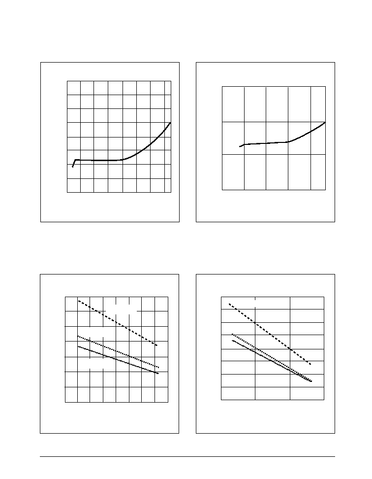
5
SP6828DS/11 SP6828/6829 +3V Low Power Voltage Inverter © Copyright 2000 Sipex Corporation
Figure 3. Charge Pump Frequency vs. Supply Voltage
for the SP6828
Figure 5. Charge Pump Frequency vs. Temperature
for the SP6828
Figure 6. Charge Pump Frequency vs. Temperature
for the SP6829
TYPICAL PERFORMANCE CHARACTERISTICS
V
IN
= +3.3V, C1 = C2 = C3 = 10
µ
F for SP6828, C1 = C2 = C3 = 3.3
µ
F for SP6829, and T
AMB
= 25
o
C unless
otherwise noted. The SP6828/6829 devices use the circuit found in
Figure 19 when obtaining the following typical
performance characteristics (unless otherwise noted).
Figure 4. Charge Pump Frequency vs. Supply Voltage
for the SP6829
16
15
14
13
12
11
10
9
8
0.5 1.0 1.5 2.0 2.5
4.0
V
IN
(V)
f
OUT
(kHz)
3.0 3.5
15
14
13
12
11
10
9
8
-60 -40 -20
0
20 40
Temperature (
o
C)
f
PUMP
(kHz)
60 80 100
V
IN
= 4.2V
V
IN
= 3.3V
V
IN
= 1.5V
40
35
30
25
0
1
2
3
4
Supply Voltage (V)
Pump F
requency (kHz)
41
39
37
35
33
31
29
27
25
-50
0
50
Temperature (
O
C)
Pump F
requency (kHz)
100
V
IN
= 1.5V
V
IN
= 4.2V
V
IN
= 3.3V
6
SP6828DS/11 SP6828/6829 +3V Low Power Voltage Inverter © Copyright 2000 Sipex Corporation
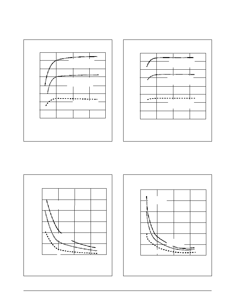
Figure 7. Output Current vs. Capacitance for the SP6828
Figure 8. Output Current vs. Capacitance for the SP6829
Figure 9. Output Voltage Ripple vs. Capacitance
for the SP6828
Figure 10. Output Voltage Ripple vs. Capacitance
for the SP6829
TYPICAL PERFORMANCE CHARACTERISTICS
V
IN
= +3.3V, C1 = C2 = C3 = 10
µ
F for SP6828, C1 = C2 = C3 = 3.3
µ
F for SP6829, and T
AMB
= 25
o
C unless
otherwise noted. The SP6828/6829 devices use the circuit found in
Figure 19 when obtaining the following typical
performance characteristics (unless otherwise noted).
40
35
30
25
20
15
10
5
0
0
10
20
Capacitance (
µ
F)
I
OUT
(mA)
30
40
V
IN
= 4.2V;
V
OUT
= -3.2V
V
IN
= 3.3V;
V
OUT
= -2.5V
V
IN
= 2V;
V
OUT
= -1.5V
600
500
400
300
200
100
0
0
10
20
Capacitance (
µ
F)
Ripple (mV)
30
40
V
IN
= 4.2V;
V
OUT
= -3.2V
V
IN
= 3.3V;
V
OUT
= -2.5V
V
IN
= 2V;
V
OUT
= -1.5V
40
35
30
25
20
15
10
5
0
0
10
20
Capacitance (
µ
F)
Output Current (mA)
30
40
V
IN
= 4.2V;
V
OUT
= -3.2V
V
IN
= 3.3V;
V
OUT
= -2.5V
V
IN
= 2V;
V
OUT
= -1.5V
300
250
200
150
100
50
0
0
10
20
Capacitance (
µ
F)
Output Ripple (mVp-p)
30
40
V
IN
= 2V;
V
OUT
= -1.5V
V
IN
= 3.3V;
V
OUT
= -2.5V
V
IN
= 4.2V;
V
OUT
= -3.2V
7
SP6828DS/11 SP6828/6829 +3V Low Power Voltage Inverter © Copyright 2000 Sipex Corporation
TYPICAL PERFORMANCE CHARACTERISTICS
V
IN
= +3.3V, C1 = C2 = C3 = 10
µ
F for SP6828, C1 = C2 = C3 = 3.3
µ
F for SP6829, and T
AMB
= 25
o
C unless
otherwise noted. The SP6828/6829 devices use the circuit found in
Figure 19 when obtaining the following typical
performance characteristics (unless otherwise noted).
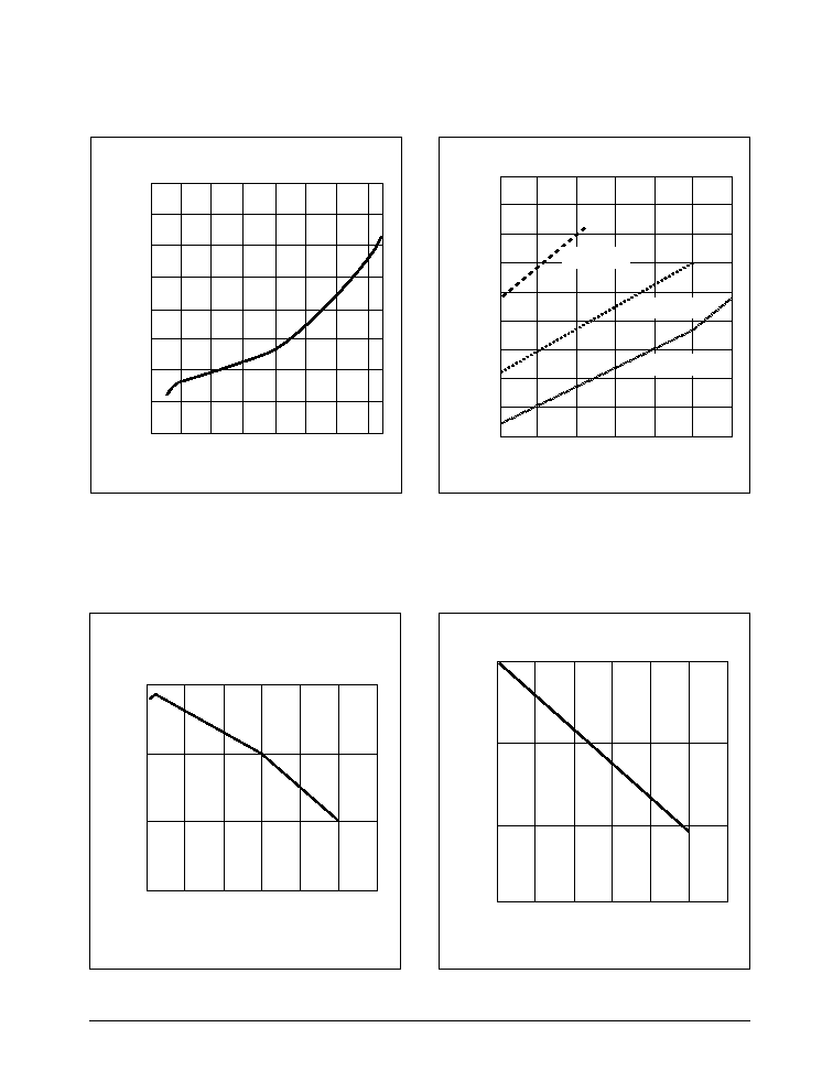
Figure 14. Voltage Efficiency vs. Output Current
Figure 11. SP6828 Supply Current vs. Supply Voltage
Figure 12. Output Voltage vs. Output Current
Figure 13. Power Efficiency vs. Output Current
40
35
30
25
20
15
10
5
0
0.5 1.0 1.5 2.0 2.5
4.0
V
IN
(V)
I
IN
(
µ
A)
3.0 3.5
0.0
-0.5
-1.0
-1.5
-2.0
-2.5
-3.0
-3.5
-4.0
-4.5
0
10
20
30
I
OUT
(mA)
V
OUT
(V)
40
50
60
V
IN
= 2V
V
IN
= 3.3V
V
IN
= 4.2V
100
90
80
70
0
5
10
15
20
I
OUT
(mA)
P
o
w
er Efficiency (%)
25
30
100
90
80
70
0
5
10
15
20
I
OUT
(mA)
V
oltage Efficiency (%)
25
30
8
SP6828DS/11 SP6828/6829 +3V Low Power Voltage Inverter © Copyright 2000 Sipex Corporation
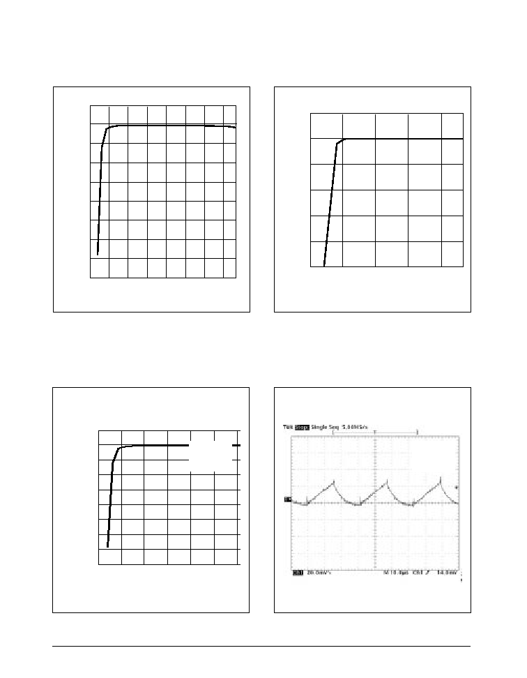
Figure 15. Voltage Efficiency vs. Supply Voltage
with a 10k
load
Figure 16. Voltage efficiency vs. Supply Voltage
without a Load
Figure 17. Output Noise and Ripple for the SP6828
TYPICAL PERFORMANCE CHARACTERISTICS
V
IN
= +3.3V, C1 = C2 = C3 = 10
µ
F for SP6828, C1 = C2 = C3 = 3.3
µ
F for SP6829, and T
AMB
= 25
o
C unless
otherwise noted. The SP6828/6829 devices use the circuit found in
Figure 19 when obtaining the following typical
performance characteristics (unless otherwise noted).
Figure 18. Output Noise and Ripple for the SP6829
102
100
98
96
94
92
90
88
86
84
0.5 1.0 1.5 2.0
V
IN
(V)
V
EFF
(%)
2.5 3.0 3.5
120
100
80
60
40
20
0
0
1
2
3
4
V
IN
(V)
V
EFF
(%)
102
100
98
96
94
92
90
88
86
84
0.5 1.0 1.5 2.0
V
IN
(V)
V
EFF
(%)
2.5 3.0 3.5 4.0
V
IN
= 3.3V
V
OUT
= -3.2V
I
L
= 5mA
V
IN
= 3.3V
V
OUT
= -3.2V
I
L
= 5mA
9
SP6828DS/11 SP6828/6829 +3V Low Power Voltage Inverter © Copyright 2000 Sipex Corporation
Figure 20. SP6828/6829 Connected as a Voltage Inverter with the load from V
OUT
to V
IN
Figure 19. SP6828/6829 in its Typical Operating Circuit as a Negative Voltage Converter; this Circuit Was Used to
Obtain the Typical Performance Characteristics Found in Figures 1 Through 18 (unless otherwise noted)
C1-
V
IN
C1+
GND
SP6828
SP6829
5
3
2
1
4
R
L
C3
C2
V
OUT
C1
C1-
V
IN
C1+
GND
SP6828
SP6829
5
3
2
1
4
C2
V
OUT
C1
R
L
C3
+
10
SP6828DS/11 SP6828/6829 +3V Low Power Voltage Inverter © Copyright 2000 Sipex Corporation
DESCRIPTION
The SP6828/6829 devices are CMOS Charge
Pump Voltage Converters that can be used to
invert a +1.15V to +4.2V input voltage. These
devices are ideal for designs involving battery-
powered and/or board level voltage conversion
applications.
The typical operating frequency of the SP6828
is 12kHz. The typical operating frequency of the
SP6829 is 35kHz. The SP6828 has a typical
operating current of 20
µ
A and the SP6829
operates at 40
µ
A. Both devices can output 25mA
with a voltage drop of 500mV. The devices are
ideal for designs using +3.3V or +3.6V lithium
ion batteries such as cell phones, PDAs, medical
instruments, and other portable equipment. The
SP6828/6829 devices combine a high efficiency
with a low quiescent current.
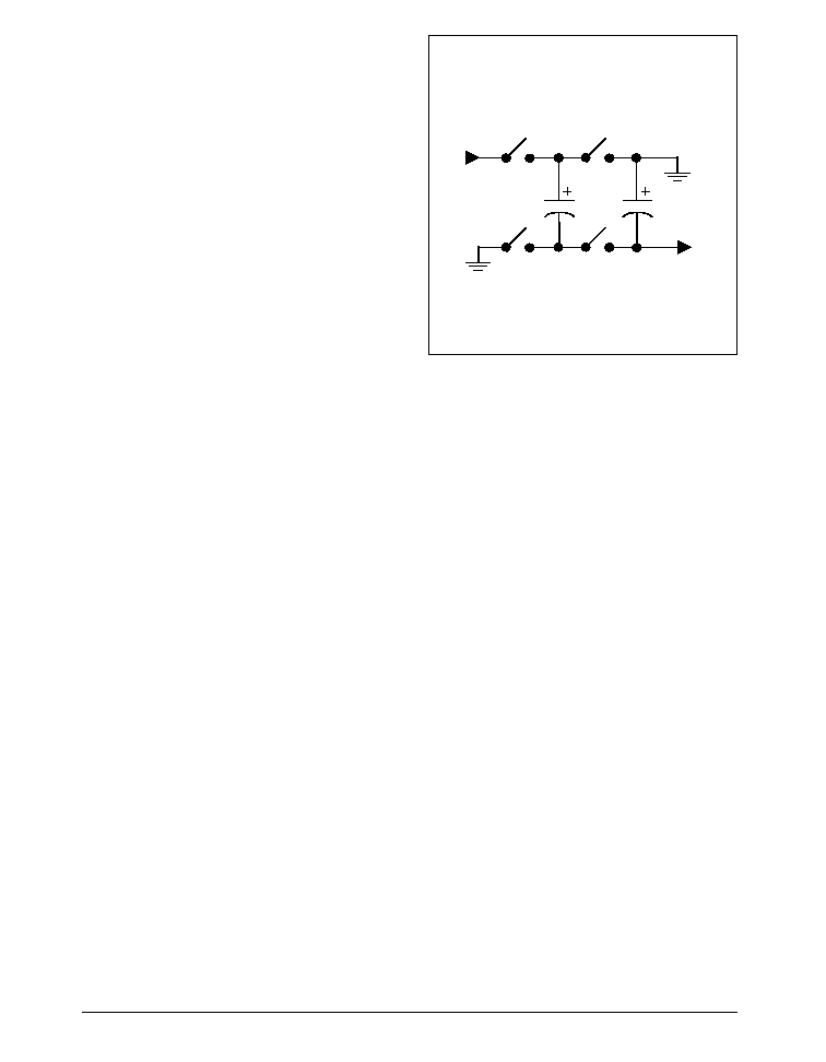
THEORY OF OPERATION
The SP6828/6829 devices should theoretically
produce an inverted input voltage. In real world
applications, there are small voltage drops at the
output that reduce efficiency. The circuit of an
ideal voltage inverter can be found in Figure 21.
The voltage inverters require two external
capacitors to store the charge. A description of
the two phases follows:
Phase 1
In the first phase of the clock cycle, switches S2
and S4 are opened and S1 and S3 closed. This
connects the flying capacitor, C1, from V
IN
to
ground. C1 charges up to the input voltage applied
at V
IN
.
Phase 2
In the second phase of the clock cycle, switches
S2 and S4 are closed and S1 and S3 are opened.
This connects the flying capacitor, C1, in parallel
with the output capacitor, C2. The charge stored
in C1 is now transferred to C2. Simultaneously,
the negative side of C2 is connected to V
OUT
and
the positive side is connected to ground. With
the voltage across C2 smaller than the voltage
across C1, the charge flows from C1 to C2 until
the voltage at the V
OUT
equals -V
IN
.
Charge-Pump Output
The output of the SP6828/6829 devices is not
regulated and therefore is dependent on the
output resistance and the amount of load current.
As the load current increases, losses may slightly
increase at the output and the voltage may become
slightly more positive. The loss at the negative
output, V
LOSS
, equals the current draw, I
OUT
, from
V
OUT
times the negative converter's source
resistance, R
S
:
V
LOSS
= I
OUT
x R
S
.
The actual inverted output voltage at V
OUT
will
equal the inverted voltage difference of V
IN
and
V
LOSS
:
V
OUT
= -(V
IN
- V
LOSS
).
Efficiency
Theoretically, the total power loss of a switched
capacitor voltage converter can be summed up as
follows:
P
LOSS
= P
INT
+ P
CAP
+ P
CONV
,
where P
LOSS
is the total power loss, P
INT
is the total
internal loss in the IC including any losses in the
MOSFET switches, P
CAP
is the resistive loss of
Figure 21. Circuit for an Ideal Voltage Inverter
C1
C2
S1
S3
S4
S2
V
OUT
V
IN
V
OUT
= -V
IN
11
SP6828DS/11 SP6828/6829 +3V Low Power Voltage Inverter © Copyright 2000 Sipex Corporation
the charge pump capacitors, and P
CONV
is the total
conversion loss during charge transfer between
the flying and output capacitors. These are the
three theoretical factors that may effect the power
efficiency of the SP6828/6829 devices in designs.
Internal losses come from the power dissipated
in the IC's internal circuitry.
Losses in the charge pump capacitors will be
induced by the capacitors' ESR. The effects of
the ESR losses and the output resistance can be
found in the following equation:
I
OUT
2
x R
OUT
= P
CAP
+ P
CONV
and
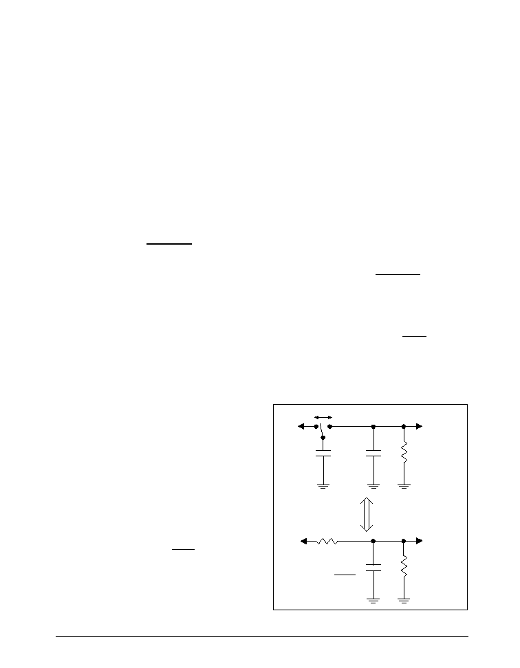
R
OUT
4 x (2 x R
SWITCHES
+ ESR
C1
) +
ESR
C2
+
1
f
OSC
x C1
,
where I
OUT
is the output current, R
OUT
is the
circuit's output resistance, R
SWITCHES
is the internal
resistance of the MOSFET switches, ESR
C1
and
ESR
C2
are the ESR of their respective capacitors,
and f
OSC
is the oscillator frequency. This term
with f
OSC
is derived from an ideal switched-
capacitor circuit as seen in Figure 22.
Conversion losses will happen during the charge
transfer between the flying capacitor, C1, and
the output capacitor, C2, when there is a voltage
difference between them. P
CONV
can be determined
by the following equation:
P
CONV
= f
OSC
x [
1
/
2
x C1 x (V
IN
2
- V
OUT
2
) +
1
/
2
x C2 x (V
RIPPLE
2
- 2 x V
OUT
x V
RIPPLE
) ].
Actual Efficiency
To determine the actual efficiency of the SP6828/
6829 device operation, a designer can use the
following equation:
Efficiency (ACTUAL) = x 100%
P
OUT
P
IN
,
where
P
OUT
= V
OUT
x I
OUT
and
P
IN
= V
IN
x I
IN
where P
OUT
is the power output, V
OUT
is the
output voltage, I
OUT
is the output current, P
IN
is
the power from the supply driving the SP6828/
6829 devices, V
IN
is the supply input voltage, and
I
IN
is the supply input current.
Ideal Efficiency
The ideal efficiency is not the true power
efficiency because it is not calculated relative to
the input power which includes the input current
losses in the charge pump. The ideal efficiency
can be determined with the following equation:
Efficiency (IDEAL) = x 100%
P
OUT
P
OUT (IDEAL)
,
where
P
OUT (IDEAL)
= -V
IN
x
-V
IN
R
L
,
and P
OUT
is the measured power output. Both
efficiencies are provided to designers for
comparison.
Figure 22. Equivalent Circuit for an Ideal Switched
Capacitor
V+
C2
R
L
V
OUT
C1
f
V+
C2
R
L
V
OUT
R
equivalent
=
1
f x C1
R
equivalent

12
SP6828DS/11 SP6828/6829 +3V Low Power Voltage Inverter © Copyright 2000 Sipex Corporation
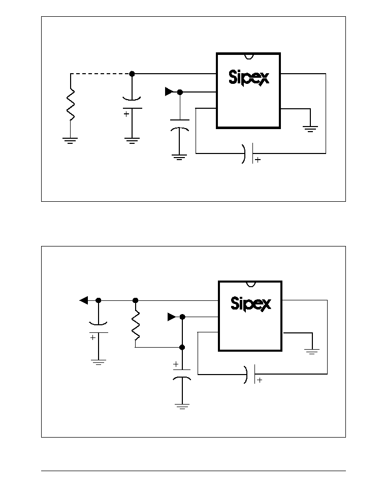
Negative Voltage Converter
The typical operating circuit for the SP6828/
6829 devices is a negative voltage converter.
Refer to Figure 19. This circuit is used to obtain
the Typical Performance Characteristics found
in Figures 1 to 18 (unless otherwise noted).
Voltage Inverter with the Load from
V
OUT
to V
IN
A designer can find the most common application
for the SP6828/6829 devices in Figure 20 as a
voltage inverter. The only external components
needed are 3 capacitors: the flying capacitor, C1,
the output capacitor, C2, and the bypass capacitor,
C3 (if necessary).
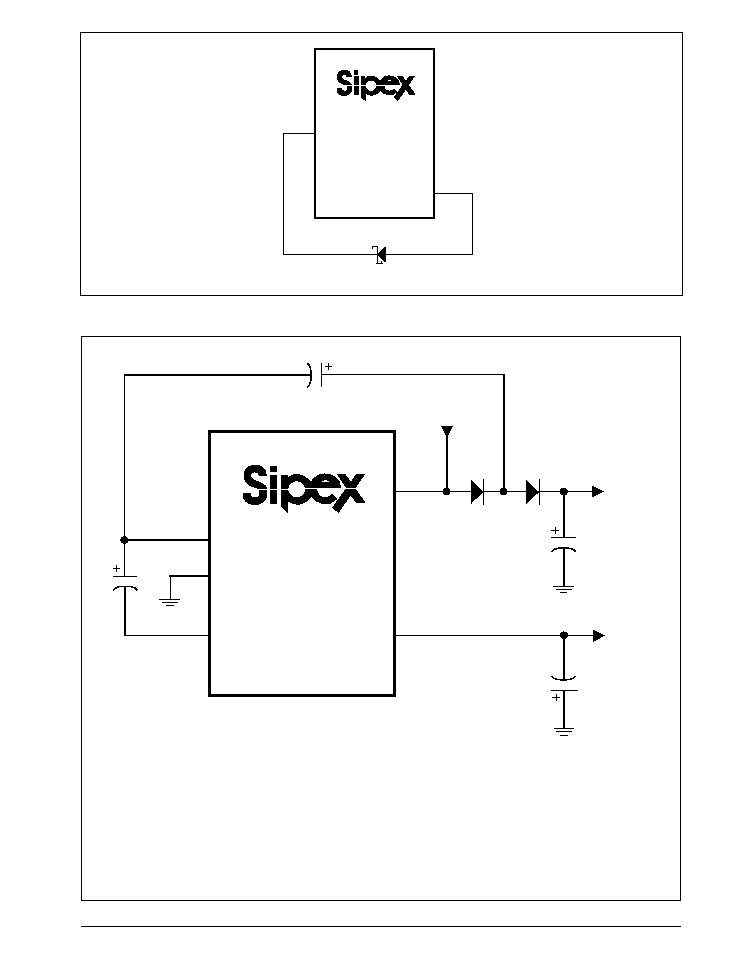
Driving Excessive Loads
The output should never be pulled above ground.
A designer should implement a Schottky diode
(1N5817) from OUT to GND when driving
heavy loads where a higher supply is sourcing
current into OUT. Refer to Figure 23 for this
circuit connection.
APPLICATION INFORMATION
For the following applications, C1 = C2 = 10
µ
F
for the SP6828 and C1 = C2 = 3.3
µ
F for the
SP6829.
Capacitor Selection
Low ESR capacitors are needed to obtain low
output resistance. Refer to Table 1 for some
suggested low ESR capacitors. The output
resistance of the SP6828/6829 devices is a
function of the ESR of C1 and C2. This output
resistance can be determined by the equation
previously provided in the Efficiency
section:
R
OUT
4 x (2 x R
SWITCHES
+ ESR
C1
) +
ESR
C2
+
1
f
OSC
x C1
,
where R
OUT
is the circuit output resistance,
R
SWITCHES
is the internal resistance of the MOSFET
switches, ESR
C1
and ESR
C2
are the ESR of their
respective capacitors, and f
OSC
is the oscillator
frequency. This term with f
OSC
is derived from an
ideal switched-capacitor circuit as seen in
Figure 21.
Minimizing the ESR of C1 and C2 will minimize
the total output resistance and will improve the
efficiency.
Flying Capacitor
Decreasing flying capacitor, C1, values will
increase the output resistance of the SP6828/
6829 devices while increasing C1 will reduce the
output resistance. There is a point where
increasing C1 will have a negligible effect on the
output resistance due to the the domination of the
output resistance by the internal MOSFET switch
resistance and the total capacitor ESR.
Output Capacitor
Increasing output capacitor, C2, values will
decrease the output ripple voltage. Reducing the
ESR of C2 will reduce both output ripple voltage
and output resistance. If higher output ripple can
be tolerated in designs, smaller capacitance values
for C2 should be used with light loads. The
following equation can be used to calculate the
peak-to-peak ripple voltage:
V
RIPPLE
= 2 x I
OUT
x ESR
C2
+
I
OUT
f
OSC
x C2
.
Input Bypass Capacitor
The bypass capacitor at the input pin will reduce
AC impedance and the impact of any of the
SP6828/6829 devices' switching noise. It is
recommended that for heavy loads a bypass
capacitor approximately equal to the flying
capacitor, C1, be used. For light loads, the value
of the bypass capacitor can be reduced.
When loading the SP6828/6829 devices from IN
to OUT, the input current remains constant
(disregarding any spikes due to internal
switching). Implementing a 0.1
µ
F bypass
capacitor should be sufficient.
When loading the SP6828/6829 devices from
OUT to GND, the current from the supply will
flow into the input for half of the cycle and will
be zero for the other half of the cycle. Designers
should implement a large bypass capacitor
(C3 = C1) if the supply has a high AC impedance.
13
SP6828DS/11 SP6828/6829 +3V Low Power Voltage Inverter © Copyright 2000 Sipex Corporation
OUT
SP6828
SP6829
C1
1
5
3
C2
C1+
C1-
GND
2
4
C4
C3
IN
D1
D2
+V
IN
V
OUT1
= (2 x V
IN
) - V
FD1
- V
FD2
V
OUT2
= -V
IN
V
OUT1
V
OUT2
where
V
OUT1
= positive doubled output voltage,
V
IN
= input voltage,
V
FD1
= forward bias voltage across D1,
V
FD2
= forward bias voltage across D2, and
V
OUT2
= inverted output voltage.
D1 = D2 = 1N4148
Figure 24. SP6828/6829 Device Connected in a Doubler/Inverter Combination Circuit
Figure 23. Protection for Heavy Loads
SP6828
SP6829
1
4
OUT
GND
1N5817
14
SP6828DS/11 SP6828/6829 +3V Low Power Voltage Inverter © Copyright 2000 Sipex Corporation
Combining a Doubler and Inverter Circuit
A designer can connect a SP6828/6829 device in
a combination doubler/inverter circuit as seen in
Figure 24. The doubler uses capacitors C3 and
C4 while the inverter uses C1 and C2. Loading
either output decreases both output voltages to
GND because both the doubler and the inverter
circuits use the charge pump. Designers should
not allow the total current output from the doubler
and the inverter to exceed 40mA.
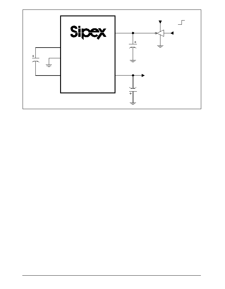
Implementing Shutdown
If shutdown control of the SP6828/6829 devices
is necessary, the circuit found in Figure 25 can
be implemented. The 0.1
µ
F capacitor at IN
absorbs transient input currents. The output
resistance of the devices can be determined by
the following equation:
R
OUT
= 20 + 2 x R
BUFFER
,
where R
OUT
is the output resistance and R
BUFFER
is the output resistance of the buffer driving IN.
R
BUFFER
can be reduced by connecting multiple
buffers in parallel at IN. The polarity of the
SHUTDOWN signal can be changed by using a
noninverting buffer to drive IN.
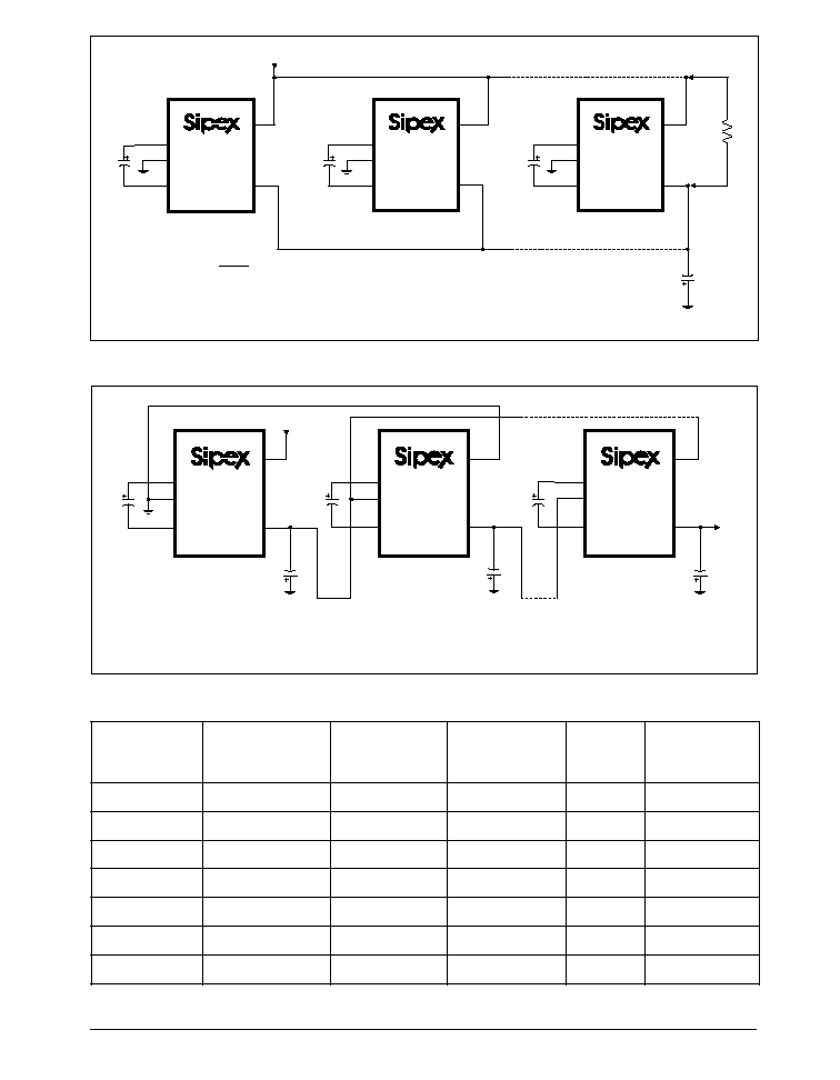
Connecting in Parallel
A designer can parallel a number of SP6828/
6829 devices to reduce the output resistance for
specific designs. All devices will need their own
flying capacitor, C1, but a single output capacitor
will serve all of the devices connected in parallel
by increasing the capacitance of C2 by a factor of
n where n equals the total number of devices
connected. This connection can be found in
Figure 26.
Cascading Devices
A designer can cascade SP6828/6829 devices to
produce a larger inverted voltage output. Refer
to Figure 27 for this circuit connection. With
two cascaded devices, the unloaded output
voltage is decreased by the output resistance of
the first device multiplied by the quiescent current
of the second device connected. The total output
resistance is greatly increased when more than
two devices are cascaded.
Layout and Grounding
Designers should make an effort to minimize
noise by paying special attention to the circuit
layout with the SP6828/6829 devices. External
components should be connected in close
proximity to the device and a ground plane
should be implemented. This will keep electrical
traces short minimizing parasitic inductance and
capacitance.
Figure 25. SP6828/6829 Device with Shutdown Control
OUT
SP6828
SP6829
C1
1
5
3
C2
C1+
C1-
GND
2
4
IN
+V
IN
V
OUT
C
IN
0.1
µ
F
Shutdown
Logic
OFF
ON
15
SP6828DS/11 SP6828/6829 +3V Low Power Voltage Inverter © Copyright 2000 Sipex Corporation
OUT
SP6828
SP6829
+V
IN
C1
5
5
3
C2
C1+
C1-
GND
2
4
OUT
SP6828
SP6829
IN
C1
1
5
3
C2
C1+
C1-
GND
2
4
OUT
SP6828
SP6829
IN
C1
1
3
5
C2
C1+
C1-
GND
2
4
V
OUT
"n"
"1"
"2"
V
OUT
= -n x V
IN
where V
OUT
= output voltage,
V
IN
= input voltage, and
n = the total number of devices connected.
IN
Figure 27. SP6828/6829 Devices Cascaded to Increase Output Voltage
OUT
SP6828
SP6829
+V
IN
C1
1
5
3
C1+
C1-
GND
2
4
OUT
SP6828
SP6829
IN
C1
1
5
3
C1+
C1-
GND
2
4
OUT
SP6828
SP6829
IN
C1
1
5
3
C2 x n
C1+
C1-
GND
2
4
R
L
"n"
"1"
"2"
where V
OUT
= output voltage
,
V
IN
= input voltage,
R
TOT
= total resistance of the devices connected in parallel,
R
OUT
= the output resistance of a single device, and
n = the total number of devices connected in parallel.
IN
R
TOT
=
R
OUT
n
V
OUT
= -V
IN
V
OUT
Figure 26. SP6828/6829 Devices Connected in Parallel to Reduce Total Output Resistance
T
R
A
P
X
E
P
I
S
R
E
B
M
U
N
R
E
R
U
T
C
A
F
U
N
A
M
R
E
B
M
U
N
T
R
A
P
/
E
C
N
A
T
I
C
A
P
A
C
E
G
A
T
L
O
V
R
S
E
X
A
M
z
H
k
0
0
1
@
E
G
A
K
C
A
P
8
2
8
6
P
S
X
V
A
5
2
0
*
6
0
1
C
S
P
T
0
1
µ
V
5
2
/
F
5
.
0
C
e
s
a
C
M
S
8
2
8
6
P
S
E
U
G
A
R
P
S
5
3
0
X
6
0
1
D
3
9
5
0
1
µ
V
5
3
/
F
3
.
0
D
e
s
a
C
M
S
8
2
8
6
P
S
T
E
M
E
K
0
2
0
*
6
0
1
C
4
9
4
T
0
1
µ
V
0
2
/
F
5
.
0
C
e
s
a
C
M
S
8
2
8
6
P
S
N
O
C
S
O
-
O
Y
N
A
S
C
6
1
0
0
X
6
0
1
C
S
4
9
0
1
µ
V
6
1
/
F
5
1
.
0
C
e
s
a
C
l
a
i
d
a
R
9
2
8
6
P
S
T
E
M
E
K
0
2
0
*
5
3
3
B
4
9
4
T
3
.
3
µ
V
0
2
/
F
5
.
1
B
e
s
a
C
M
S
9
2
8
6
P
S
E
U
G
A
R
P
S
5
3
0
0
X
5
3
3
D
5
9
5
3
.
3
µ
V
5
3
/
F
0
.
2
C
e
s
a
C
M
S
9
2
8
6
P
S
N
O
C
S
O
-
O
Y
N
A
S
A
6
1
0
0
X
5
3
3
C
S
4
9
3
.
3
µ
V
6
1
/
F
5
3
.
0
A
e
s
a
C
l
a
i
d
a
R
Table 1. Suggested Low ESR Tantalum Capacitors
16
SP6828DS/11 SP6828/6829 +3V Low Power Voltage Inverter © Copyright 2000 Sipex Corporation
PACKAGE: SOT23-5
SYMBOL
A
A1
A2
b
C
D
E
E1
L
e
e1
a
1.45
0.15
1.30
0.50
0.20
3.10
3.00
1.75
0.55
10
O
0.90
0.00
0.90
0.25
0.09
2.80
2.60
1.50
0.35
0
O
MIN
MAX
0.95ref
1.90ref
E
A
e
C
L
b
e1
D
C
L
A2
A1
A
A
.10
C
L
E1
L
2
0.20
DATUM 'A
'
C
a
17
SP6828DS/11 SP6828/6829 +3V Low Power Voltage Inverter © Copyright 2000 Sipex Corporation
ORDERING INFORMATION
Model
Temperature Range
Package Type
SP6828EK . ............................................ -40∞C to +85∞C ............................................... SOT23-5
SP6828-5EK ........................................... -40∞C to +85∞C ............................................... SOT23-5
SP6828EK/TR ......................................... -40∞C to +85∞C ............................................... SOT23-5
SP6828-5EK/TR ..................................... -40∞C to +85∞C ............................................... SOT23-5
SP6829EK . ............................................ -40∞C to +85∞C ............................................... SOT23-5
SP6829EK/TR ......................................... -40∞C to +85∞C ............................................... SOT23-5
Corporation
SIGNAL PROCESSING EXCELLENCE
Sipex Corporation reserves the right to make changes to any products described herein. Sipex does not assume any liability arising out of the
application or use of any product or circuit described hereing; neither does it convey any license under its patent rights nor the rights of others.
Please consult the factory for pricing and availability on a Tape-On-Reel option.
Sipex Corporation
Headquarters and
Sales Office
22 Linnell Circle
Billerica, MA 01821
TEL: (978) 667-8700
FAX: (978) 670-9001
e-mail: sales@sipex.com
Sales Office
233 South Hillview Drive
Milpitas, CA 95035
TEL: (408) 934-7500
FAX: (408) 935-7600