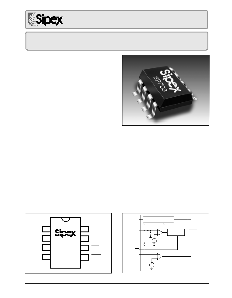
 | –≠–ª–µ–∫—Ç—Ä–æ–Ω–Ω—ã–π –∫–æ–º–ø–æ–Ω–µ–Ω—Ç: SP704 | –°–∫–∞—á–∞—Ç—å:  PDF PDF  ZIP ZIP |
SP703/704DS/07
SP703/704 Low Power Microprocessor Supervisory
© Copyright 2000 Sipex Corporation
1
SP703/SP704
Low Power Microprocessor Supervisory
with Battery Switch-Over
The SP703/704 devices are microprocessor (
µ
P) supervisory circuits that integrate a myriad
of components involved in discrete solutions to monitor power-supply and battery-control
functions in
µ
P and digital systems. The series will significantly improve system reliability and
operational efficiency when compared to discrete solutions. The features of the SP703/704
devices include a manual reset input, a
µ
P reset and backup-battery switchover, and power-
failure warning. The series is ideal for applications in computers, controllers, intelligent
instruments and automotive systems. All designs where it is critical to monitor the power
supply to the
µ
P and its related digital components will find the series to be an ideal solution.
s
Precision Voltage Monitor:
SP703 at 4.65V
SP704 at 4.40V
s
Reset Time Delay - 200ms
s
Debounced TTL/CMOS -
Compatible Manual - Reset Input
s
Minimum component count
s
60
µ
A Maximum Operating Supply Current
s
0.6
µ
A Maximum Battery Backup Current
s
0.1
µ
A Maximum Battery Standby Current
s
Power Switching
250mA Output in V
CC
Mode (0.6
)
25mA Output in Battery Mode (5
)
s
Voltage Monitor for Power Fail or
Low Battery Warning
s
Available in 8 pin SO and DIP packages
s
RESET asserted down to V
CC
= 1V
s
Pin Compatible Upgrades to
MAX703/MAX704
DESCRIPTION
PINOUT
V
OUT
V
CC
GND
PFI
V
BATT
RESET
MR
PFO
1
2
3
4
5
6
7
8
INTERNAL BLOCK DIAGRAM
1.25V
1.25V
BATTERY SWITCHOVER
CIRCUITRY
PFI
MR
V
CC
V
BATT
RESET
GENERATOR
V
OUT
RESET
PFO
Æ
SP703/704DS/07
SP703/704 Low Power Microprocessor Supervisory
© Copyright 2000 Sipex Corporation
2
ABSOLUTE MAXIMUM RATINGS
These are stress ratings only and functional operation
of the device at these ratings or any other above those
indicated in the operation sections of the specifica-
tions below is not implied. Exposure to absolute maxi-
mum rating conditions for extended periods of time
may affect reliability and cause permanent damage to
the device.
V
CC
........................................................-0.3V to 6.0V
V
BATT
.....................................................-0.3V to 6.0V
All Other Inputs......................................-0.3V to (V
CC
+0.3V)
Input Current:
V
CC
.........................................................250mA
V
BATT
........................................................50mA
GND........................................................20mA
Output Current:
V
OUT
.....Short-Circuit Protected for up to 10sec
All Other Inputs.................................20mA
Rate of Rise, V
CC
,V
BATT
..................100V/
µ
s
Continuous Power Dissipation.......500mW
Storage Temperature.......-65
∞
C to +160
∞
C
Lead Temperature(soldering,10sec).................+300
∞
C
ESD Rating.............................4kV Human Body Model
SPECIFICATIONS
V
cc
=4.75v to 5.50V for SP703, V
CC
= 4.50V to 5.50V for SP704, V
BATT
=2.80V, T
A
=T
MIN
to T
MAX
, typical specified at 25
O
C, unless otherwise noted.
S
R
E
T
E
M
A
R
A
P
.
N
I
M
.
P
Y
T
.
X
A
M
S
T
I
N
U
S
N
O
I
T
I
D
N
O
C
,
e
g
n
a
R
e
g
a
t
l
o
V
g
n
i
t
a
r
e
p
O
0
5
.
5
s
t
l
o
V
V
C
C
V
r
o
T
T
A
B
1
E
T
O
N
,
I
,
t
n
e
r
r
u
C
y
l
p
p
u
S
Y
L
P
P
U
S
,
5
3
0
6
µ
A
I
g
n
i
d
u
l
c
x
e
T
U
O
I
Y
L
P
P
U
S
,
e
d
o
M
p
u
k
c
a
B
y
r
e
t
t
a
B
n
i
V
C
C
V
,
V
0
=
T
T
A
B
V
8
.
2
=
1
0
0
.
0
6
.
0
µ
A
V
T
T
A
B
2
E
T
O
N
,
t
n
e
r
r
u
C
y
b
d
n
a
t
S
1
.
0
-
2
0
.
0
µ
A
V
C
C
V
>
T
T
A
B
V
2
.
0
+
V
T
U
O
t
u
p
t
u
O
V
C
C
1
.
0
-
V
C
C
3
0
.
0
-
V
C
C
5
1
.
0
-
s
t
l
o
V
I
T
U
O
A
m
0
5
=
I
T
U
O
A
m
0
5
2
=
V
T
U
O
e
d
o
M
p
u
k
c
a
B
-
y
r
e
t
t
a
B
n
i
V
C
C
V
<
T
T
A
B
V
2
.
0
-
V
T
T
A
B
5
1
.
0
-
V
T
T
A
B
4
0
.
0
-
V
T
T
A
B
0
2
.
0
-
s
t
l
o
V
I
T
U
O
A
m
5
=
I
T
U
O
A
m
5
2
=
,
d
l
o
h
s
e
r
h
T
h
c
t
i
w
S
y
r
e
t
t
a
B
V
C
C
V
o
t
T
T
A
B
0
2
0
2
-
V
m
p
u
-
r
e
w
o
P
n
w
o
d
-
r
e
w
o
P
s
i
s
e
r
e
t
s
y
H
r
e
v
o
h
c
t
i
w
S
y
r
e
t
t
a
B
0
4
V
m
k
a
e
P
o
t
k
a
e
P
d
l
o
h
s
e
r
h
T
t
e
s
e
R
0
5
.
4
5
2
.
4
5
6
.
4
0
4
.
4
5
7
.
4
0
5
.
4
s
t
l
o
V
3
0
7
P
S
4
0
7
P
S
SP703/704DS/07
SP703/704 Low Power Microprocessor Supervisory
© Copyright 2000 Sipex Corporation
3
S
R
E
T
E
M
A
R
A
P
.
N
I
M
.
P
Y
T
.
X
A
M
S
T
I
N
U
S
N
O
I
T
I
D
N
O
C
s
i
s
e
r
e
t
s
y
H
d
l
o
h
s
e
r
h
T
t
e
s
e
R
0
4
V
m
k
a
e
P
o
t
k
a
e
P
t
,
h
t
d
i
W
e
s
l
u
P
t
e
s
e
R
S
R
0
4
1
0
0
2
0
8
2
s
m
e
g
a
t
l
o
V
t
u
p
t
u
O
T
E
S
E
R
V
C
C
5
.
1
-
I
E
C
R
U
O
S
0
0
8
=
µ
A
1
.
0
4
0
0
.
0
4
.
0
3
.
0
s
t
l
o
V
I
K
N
I
S
A
m
2
.
3
=
I
K
N
I
S
0
5
=
µ
V
,
A
C
C
V
0
.
1
=
d
l
o
h
s
e
r
h
T
t
u
p
n
I
R
M
W
O
L
H
G
I
H
0
.
2
8
.
0
V
h
t
d
i
W
e
s
l
u
P
m
u
m
i
n
i
M
R
M
0
5
1
s
n
y
a
l
e
D
T
E
S
E
R
o
t
R
M
0
5
2
s
n
t
n
e
r
r
u
C
p
U
ll
u
P
R
M
0
0
1
0
5
2
0
0
6
A
µ
V
0
=
R
M
d
l
o
h
s
e
r
h
T
t
u
p
n
I
I
F
P
0
0
2
.
1
0
5
2
.
1
0
0
3
.
1
s
t
l
o
V
t
n
e
r
r
u
C
t
u
p
n
I
I
F
P
5
2
-
1
0
.
0
5
2
A
n
e
g
a
t
l
o
V
t
u
p
t
u
O
O
F
P
V
C
C
5
.
1
-
1
.
0
4
.
0
s
t
l
o
V
I
E
C
R
U
O
S
0
0
8
=
µ
A
I
K
N
I
S
A
m
2
.
3
=
NOTE 1: Either V
CC
or V
BATT
can go to 0V if the other is greater than 2.0V.
NOTE 2: "-" equals the battery-charging current, "+" equals the battery-discharging current.
SPECIFICATIONS (continued)
V
cc
=4.75V to 5.50V for SP703, V
CC
= 4.5 0V to 5.50V for SP704, V
BATT
=2.80V, T
A
=T
MIN
to T
MAX
, typical specified at 25
O
C, unless otherwise noted.
SP703/704DS/07
SP703/704 Low Power Microprocessor Supervisory
© Copyright 2000 Sipex Corporation
4
PIN ASSIGNMENTS
Pin 1 --V
OUT
-- Output Supply Voltage. V
OUT
connects to V
CC
when V
CC
is greater than
V
BATT
and V
CC
is above the reset thresh-
old. When V
CC
falls below V
BATT
and
V
CC
is below the reset threshold, V
OUT
connects to V
BATT
. Connect a 0.1
µ
F ca-
pacitor from V
OUT
to GND.
Pin 2 -- V
CC
-- +5V Supply Input
Pin3 -- GND -- Ground reference for all signals
Pin 4 -- PFI -- Power-Fail Input. This is the
noninverting input to the power-fail com-
parator. When PFI is less than 1.25V,
PFO goes low. Connect PFI to GND or
V
OUT
when not used.
Pin 5 -- PFO -- Power-Fail Output.
Pin 6 -- MR -- Manual Reset Input. This input
generates a reset pulse when pulled below
0.8V. This active LOW input is TTL/
CMOS compatible and can be shorted to
ground with a switch. It has an internal
250
µ
A (typical) pull-up current. Leave
this pin floating when not used.
Pin 7 -- RESET (Active Low)≠ Reset Output.
RESET Output goes low whenever
V
CC
falls below the reset threshold or
whenever MR is pulled below 0.8V for
longer than 150nS. RESET remains low
for 200ms after V
CC
crosses the reset
threshold voltage on power-up or after
being triggered by MR.
Pin 8 -- V
BATT
-- Backup-Battery Input. When
V
CC
falls below the reset threshold, V
BATT
will be switched to V
OUT
if V
BATT
is
20mV greater than V
CC
. When V
CC
rises
20mV above V
BATT
, V
OUT
will be recon-
nected to V
CC
. The 40mV hysteresis pre-
vents repeated switching if V
CC
falls
slowly.
PINOUT
INTERNAL BLOCK DIAGRAM
V
OUT
V
CC
GND
PFI
V
BATT
RESET
MR
PFO
1
2
3
4
5
6
7
8
1.25V
1.25V
BATTERY SWITCHOVER
CIRCUITRY
PFI
MR
V
CC
V
BATT
RESET
GENERATOR
V
OUT
RESET
PFO

SP703/704DS/07
SP703/704 Low Power Microprocessor Supervisory
© Copyright 2000 Sipex Corporation
5
V
CC
Supply Current vs.
Temperature (Normal Mode)
Battery Supply Current vs.
Temperature (Backup Mode)
51
47
43
39
35
31
27
23
19
-60 -30 0 30
60 90 120 150
V
CC
Current (
µ
A)
Temperature Deg. C
2.9
2.4
1.9
1.4
0.9
0.4
-0.1
V
BATT
Current (
µ
A)
-60
Temperature Deg. C
-40 -20
0 20 40 60 80 100 120 140
V
CC
=5V
V
BATT
=2.8V
V
CC
=0V
V
BATT
=2.8V
TYPICAL CHARACTERISTICS
(25
o
C, unless otherwise noted)
-60 -30 0 30
60 90 120 150
Temperature Deg. C
PFI Threshold
vs. Temperature
1.256
1.254
1.252
1.250
1.248
1.246
PFI Threshold (V)
V
CC
=5V
V
BATT
=0
NO LOAD ON PFO
V
BATT
to V
OUT
ON
Resistance vs. Temperature
V
CC
to V
OUT
On
Resistance vs. Temperature
15
10
5
0
Resistance (ohms)
-60 -30 0 30 60 90 120 150
Temperature Deg. C
0.9
0.8
0.7
0.6
0.5
0.4
0.3
Resistance (ohms)
Temperature Deg. C
V
BATT
=2.8V
V
BATT
=4.5V
V
CC
=0V V
BATT
=2V
Reset Threshold
vs. Temperature
4.70
4.69
4.68
4.67
4.66
4.65
4.64
4.63
4.62
4.61
4.60
Reset Threshold (V)
Temperature Deg. C
V
BATT
=0V
Power Down
V
CC
=5V
V
BATT
=0V
Reset Output Resistance
vs. Temperature
Reset Delay
vs. Temperature
600
500
400
300
200
100
0
Resistance (ohms)
-60 -30 0 30
60 90 120 150
Temperature Deg. C
212
210
208
206
204
202
200
Reset Delay (mS)
-60 -30 0 30
60 90 120 150
Temperature Deg. C
V
CC
=5V,V
BATT
=2.8V
Soucing Current
V
CC
=0V to 5V Step,
V
BATT
=2.8V
V
CC
=0V,V
BATT
=2.8V
Sink Current
IE+2
IE+1
IE+0
IE-1
IE-2
IE-3
IE-4
IE-5
IE-6
IE-7
IE-8
V
BATT
Current(
µ
A) Log Scale
.0000 5.000
V
CC
(0.5V/div)
Battery Current vs. V
CC
Voltage
V
BATT
=2.8V
SP703
-60 -30 0 30 60 90 120 150
-60 -30 0 30 60 90 120 150