SP706-708 Final Rev. 9-13-00
1
Rev. 10-17-00 SP706 +3.0/ +3.3 Low Power Microprocessor Circuits © Copyright 2000 Sipex Corporation
SP706P/R/S/T, SP708R/S/T
s
Precision Low Voltage Monitor:
SP706P/R and SP708R at +2.63V
SP706S and SP708S at +2.93V
SP706T and SP708T at +3.08V
s
RESET Pulse Width - 200ms
s
Independent Watchdog Timer - 1.6 sec
Timeout (SP706P/S/R/T)
s
40
µ
A Maximum Supply Current
s
Debounced TTL/CMOS Manual-Reset Input
s
RESET Asserted Down to V
CC
= 1V
s
RESET Output:
SP706P Active-High
SP706R/S/T Active-Low
SP708R/S/T Both Active High + Active Low
s
WDI Can Be Left Floating, Disabling the
Watchdog Function
DESCRIPTION
The SP706P/S/R/T, SP708R/S/T series is a family of microprocessor (
µ
P) supervisory circuits
that integrate myriad components involved in discrete solutions which monitor power-supply and
battery, in
µ
P, and digital systems. The SP706P/S/R/T, SP708R/S/T series will significantly
improve system reliability and operational efficiency when compared to results obtained with
discrete components. The features of the SP706P/S/R/T, SP708R/S/T series include a
watchdog timer, a
µ
P reset, a Power Fail Comparator, and a manual-reset input. The SP706P/
S/R/T, SP708R/S/T series is ideal for +3.0V or +3.3V applications in automotive systems,
computers, controllers, and intelligent instruments. The SP706P/S/R/T, SP708R/S/T series is
an ideal solution for systems in which critical monitoring of the power supply to the
µ
P and related
digital components is demanded.
r
e
b
m
u
N
t
r
a
P
e
v
i
t
c
A
T
E
S
E
R
d
l
o
h
s
e
r
h
T
T
E
S
E
R
t
e
s
e
R
l
a
u
n
a
M
y
c
a
r
u
c
c
A
I
F
P
t
u
p
n
I
g
o
d
h
c
t
a
W
P
6
0
7
P
S
H
G
I
H
V
3
6
.
2
S
E
Y
%
4
S
E
Y
R
6
0
7
P
S
W
O
L
V
3
6
.
2
S
E
Y
%
4
S
E
Y
S
6
0
7
P
S
W
O
L
V
3
9
.
2
S
E
Y
%
4
S
E
Y
T
6
0
7
P
S
W
O
L
V
8
0
.
3
S
E
Y
%
4
S
E
Y
R
8
0
7
P
S
H
G
I
H
/
W
O
L
V
3
6
.
2
S
E
Y
%
4
O
N
S
8
0
7
P
S
H
G
I
H
/
W
O
L
V
3
9
.
2
S
E
Y
%
4
O
N
T
8
0
7
P
S
H
G
I
H
/
W
O
L
V
8
0
.
3
S
E
Y
%
4
O
N
s
Built-In V
cc
Glitch Immunity
s
Available in 8-pin PDIP, NSOIC, and
µ
SOIC packages
s
Voltage Monitor for Power Failure or Low
Battery Warning
s
Pin Compatible Enhancement to Industry
Standards 706P/R/S/T and 708R/S/T
+3.0V/+3.3V Low Power Microprocessor
Supervisory Circuits
®
2
Rev. 10-17-00 SP706 +3.0/ +3.3 Low Power Microprocessor Circuits © Copyright 2000 Sipex Corporation
SPECIFICATIONS
V
cc
= 2.7V to 5.5V for SP70_P/R, V
CC
= 3.0 to 5.5V for SP70_S, V
CC
= 3.15V to 5.5V for SP70_T, T
A
= T
MIN
to T
MAX
to T
MAX
, unless otherwise noted,
typical at 25
°
C.
ABSOLUTE MAXIMUM RATINGS
These are stress ratings only and functional operation
of the device at these ratings or any other above those
indicated in the operation sections of the specifications
below is not implied. Exposure to absolute maximum
rating conditions for extended periods of time may
affect reliability.
Terminal Voltage (with respect to GND):
V
CC
........................................................-0.3V to +6.0V
All Other Inputs (Note 1)..............-0.3V to (V
CC
+3.0V)
Input Current:
V
CC
.....................................................................20mA
GND...................................................................20mA
Output Current (all outputs)...............................20mA
ESD Rating...........................................................2kV
R
E
T
E
M
A
R
A
P
.
N
I
M
.
P
Y
T
.
X
A
M
S
T
I
N
U
S
N
O
I
T
I
D
N
O
C
V
,
e
g
n
a
R
e
g
a
t
l
o
V
g
n
i
t
a
r
e
p
O
C
C
0
.
1
5
.
5
V
I
,
t
n
e
r
r
u
C
y
l
p
p
u
S
Y
L
P
P
U
S
5
2
0
4
µ
A
V
=
R
M
C
C
g
n
i
t
a
o
l
F
I
D
W
,
g
n
i
t
a
o
l
F
r
o
d
l
o
h
s
e
r
h
T
t
e
s
e
R
5
5
.
2
5
8
.
2
0
0
.
3
3
6
.
2
3
9
.
2
8
0
.
3
0
7
.
2
0
0
.
3
5
1
.
3
V
R
/
P
_
0
7
P
S
S
_
0
7
P
S
T
_
0
7
P
S
s
i
s
e
r
e
t
s
y
H
d
l
o
h
s
e
r
h
T
t
e
s
e
R
0
2
V
m
2
e
t
o
N
t
,
h
t
d
i
W
e
s
l
u
P
t
e
s
e
R
S
R
0
4
1
0
0
2
0
8
2
s
m
2
e
t
o
N
T
E
S
E
R
e
g
a
t
l
o
V
t
u
p
t
u
O
V
H
O
V
L
O
V
H
O
V
L
O
V
x
8
.
0
C
C
V
C
C
5
.
1
-
3
.
0
4
.
0
V
V
)
X
A
M
(
T
S
R
V
<
C
C
I
,
V
6
.
3
<
E
C
R
U
O
S
0
0
5
=
µ
A
V
)
X
A
M
(
T
S
R
V
<
C
C
I
,
V
6
.
3
<
K
N
I
S
2
.
1
=
mA
V
<
V
5
.
4
C
C
I
,
V
5
.
5
<
E
C
R
U
O
S
0
0
8
=
µ
A
V
<
V
5
.
4
C
C
I
,
V
5
.
5
<
K
N
I
S
A
m
2
.
3
=
e
g
a
t
l
o
V
t
u
p
t
u
O
T
E
S
E
R
V
H
O
V
L
O
V
H
O
V
L
O
V
C
C
6
.
0
-
V
C
C
5
.
1
-
3
.
0
4
.
0
V
V
)
X
A
M
(
T
S
R
V
<
C
C
I
,
V
6
.
3
<
E
C
R
U
O
S
5
1
2
=
µ
A
V
)
X
A
M
(
T
S
R
V
<
C
C
I
,
V
6
.
3
<
E
C
R
U
O
S
A
m
2
.
1
=
V
<
V
5
.
4
C
C
I
,
V
5
.
5
<
E
C
R
U
O
S
0
0
8
=
µ
A
V
<
V
5
.
4
C
C
I
,
V
5
.
5
<
E
C
R
U
O
S
A
m
2
.
3
=
t
,
d
o
i
r
e
P
t
u
o
e
m
i
T
g
o
d
h
c
t
a
W
D
W
0
0
.
1
0
6
.
1
5
2
.
2
s
V
C
C
V
6
.
3
<
t
,
h
t
d
i
W
e
s
l
u
P
I
D
W
P
W
0
5
s
n
V
L
I
V
,
V
4
.
0
=
H
I
V
x
8
.
0
=
C
C
,
d
l
o
h
s
e
r
h
T
t
u
p
n
I
I
D
W
V
L
I
V
H
I
V
L
I
V
H
I
V
x
7
.
0
C
C
5
.
3
6
.
0
8
.
0
V
V
)
X
A
M
(
T
S
R
V
<
C
C
V
6
.
3
<
V
T
S
R
)
X
A
M
(
V
<
C
C
V
6
.
3
<
V
C
C
V
0
.
5
=
V
C
C
V
0
.
5
=
t
n
e
r
r
u
C
t
u
p
n
I
I
D
W
1
-
2
0
.
0
1
µ
A
V
r
o
0
=
I
D
W
C
C
Continuous Power Dissipation
Plastic DIP
(derate 9.09mW/
O
C above +70
O
C)..................727mW
SO
(derate 5.88mW/
O
C above +70
O
C)..................471mW
Mini SO
(derate 4.10mW/
O
C above +70
O
C)..................330mW
Storage Temperature Range.............-65°C to +160°C
Lead Temperature (solding 10 sec)................+300°C
3
Rev. 10-17-00 SP706 +3.0/ +3.3 Low Power Microprocessor Circuits © Copyright 2000 Sipex Corporation
SPECIFICATIONS (continued)
V
cc
= 2.7V to 5.5V for SP70_P/R, V
CC
= 3.0 to 5.5V for SP70_S, V
CC
= 3.15V to 5.5V for SP70_T, T
A
= T
MIN
to T
MAX
to T
MAX
, unless otherwise noted,
typical at 25
°
C.
R
E
T
E
M
A
R
A
P
.
N
I
M
.
P
Y
T
.
X
A
M
S
T
I
N
U
S
N
O
I
T
I
D
N
O
C
e
g
a
t
l
o
V
t
u
p
t
u
O
O
D
W
V
H
O
V
L
O
V
H
O
V
L
O
V
x
8
.
0
C
C
V
C
C
5
.
1
-
3
.
0
4
.
0
V
V
)
X
A
M
(
T
S
R
V
<
C
C
I
,
V
6
.
3
<
E
C
R
U
O
S
0
0
5
=
µ
A
V
)
X
A
M
(
T
S
R
V
<
C
C
I
,
V
6
.
3
<
K
N
I
S
A
m
2
.
1
=
V
<
V
5
.
4
C
C
I
,
V
5
.
5
<
E
C
R
U
O
S
0
0
8
=
µ
A
V
<
V
5
.
4
C
C
I
,
V
5
.
5
<
K
N
I
S
A
m
2
.
3
=
R
M
t
n
e
r
r
u
C
p
U
-
ll
u
P
5
2
0
0
1
0
7
0
5
2
0
5
2
0
0
6
µ
A
R
M
V
,
V
0
=
)
X
A
M
(
T
S
R
V
<
C
C
V
6
.
3
<
V
<
V
5
.
4
,
V
0
=
R
M
C
C
V
5
.
5
<
R
M
t
,
h
t
d
i
W
e
s
l
u
P
R
M
0
0
5
0
5
1
s
n
V
)
X
A
M
(
T
S
R
V
<
C
C
V
6
.
3
<
V
<
V
5
.
4
C
C
V
5
.
5
<
R
M
d
l
o
h
s
e
r
h
T
t
u
p
n
I
V
L
I
V
H
I
V
L
I
V
H
I
V
x
7
.
0
C
C
0
.
2
6
.
0
8
.
0
V
V
)
X
A
M
(
T
S
R
V
<
C
C
V
6
.
3
<
V
)
X
A
M
(
T
S
R
V
<
C
C
V
6
.
3
<
V
<
V
5
.
4
C
C
V
5
.
5
<
V
<
V
5
.
4
C
C
V
5
.
5
<
R
M
t
,
y
a
l
e
D
t
u
O
t
e
s
e
R
o
t
D
M
0
5
7
0
5
2
s
n
V
)
X
A
M
(
T
S
R
V
<
C
C
2
E
T
O
N
,
V
6
.
3
<
V
<
V
5
.
4
C
C
2
E
T
O
N
,
V
5
.
5
<
d
l
o
h
s
e
r
h
T
t
u
p
n
I
I
F
P
0
2
.
1
5
2
.
1
0
3
.
1
V
V
C
C
e
h
t
r
o
f
V
0
.
3
=
R
/
P
_
0
7
P
S
V
,
C
C
=
e
h
t
r
o
f
V
3
.
3
T
/
S
_
0
7
P
S
g
n
il
l
a
f
I
F
P
,
t
n
e
r
r
u
C
t
u
p
n
I
I
F
P
0
0
.
5
2
-
1
0
.
0
0
0
.
5
2
A
n
O
F
P
e
g
a
t
l
o
V
t
u
p
t
u
O
V
H
O
V
L
O
V
H
O
V
L
O
V
x
8
.
0
C
C
V
C
C
5
.
1
-
3
.
0
4
.
0
V
V
)
X
A
M
(
T
S
R
V
<
C
C
I
,
V
6
.
3
<
E
C
R
U
O
S
0
0
5
=
µ
A
V
)
X
A
M
(
T
S
R
V
<
C
C
I
,
V
6
.
3
<
K
N
I
S
2
.
1
=
mA
V
<
V
5
.
4
C
C
I
,
V
5
.
5
<
E
C
R
U
O
S
0
0
8
=
µ
A
V
<
V
5
.
4
C
C
I
,
V
5
.
5
<
K
N
I
S
A
m
2
.
3
=
4
Rev. 10-17-00 SP706 +3.0/ +3.3 Low Power Microprocessor Circuits © Copyright 2000 Sipex Corporation
SP706P/R/S/T
1
8
7
6
5
4
3
2
1
MR
V
CC
GND
PFI
WDO
RESET / RESET*
WDI
PFO
SP708S/R/T
1
8
7
6
5
4
3
2
1
MR
V
CC
GND
PFI
RESET
RESET
N.C.
PFO
*SP706P only
DIP and SOIC
1
8
7
6
5
4
3
2
1
WDO
MR
V
CC
WDI
PFO
PFI
GND
1
8
7
6
5
4
3
2
1
RESET
RESET
MR
V
CC
N.C.
PFO
PFI
GND
RESET / RESET*
SP706P/R/S/T
SP708S/R/T
*SP706P only
µ
SOIC
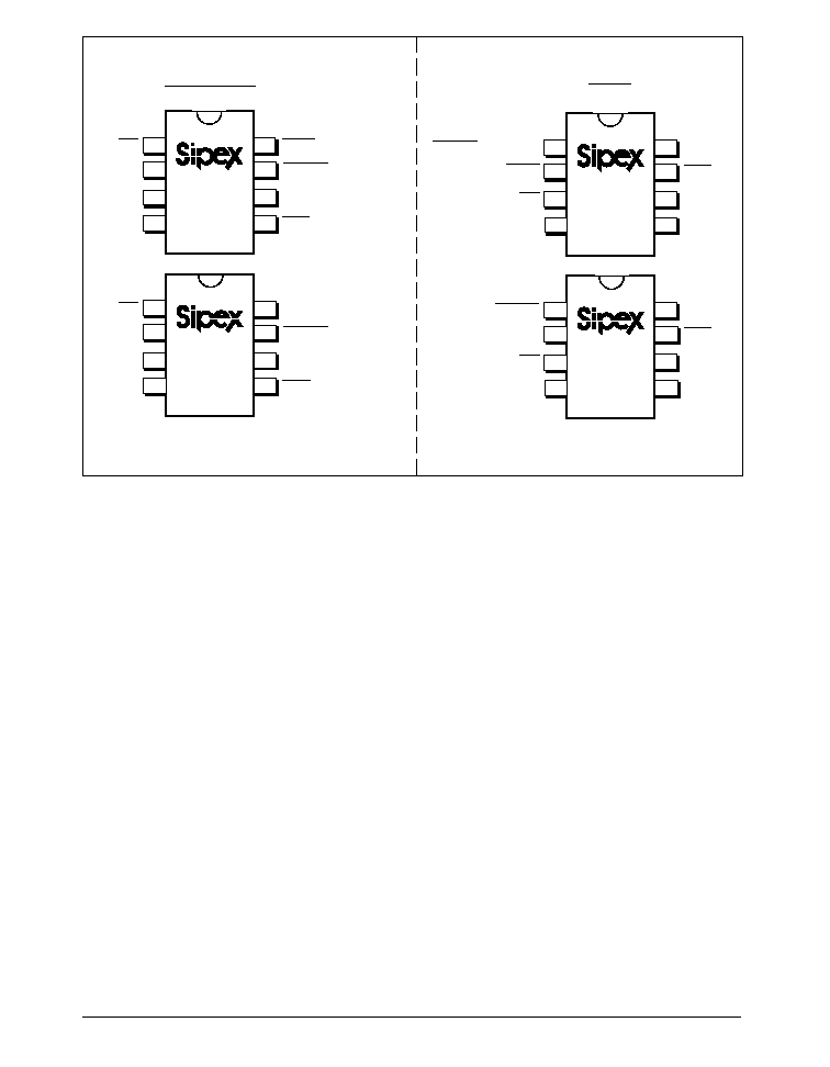
Figure 1. Pinouts
5
Rev. 10-17-00 SP706 +3.0/ +3.3 Low Power Microprocessor Circuits © Copyright 2000 Sipex Corporation
E
M
A
N
N
O
I
T
C
N
U
F
N
O
I
T
P
I
R
C
S
E
D
N
I
P
P
6
0
7
P
S
T
/
S
/
R
6
0
7
P
S
T
/
S
/
R
8
0
7
P
S
/
P
I
D
C
I
O
S
µ
C
I
O
S
/
P
I
D
C
I
O
S
µ
C
I
O
S
/
P
I
D
C
I
O
S
µ
C
I
O
S
R
M
e
s
l
u
p
t
e
s
e
r
a
s
r
e
g
g
i
r
t
t
u
p
n
i
s
i
h
T
-
t
e
s
e
R
l
a
u
n
a
M
t
u
p
n
i
W
O
L
-
e
v
i
t
c
a
s
i
h
T
.
V
8
.
0
w
o
l
e
b
d
e
ll
u
p
n
e
h
w
0
7
l
a
n
r
e
t
n
i
n
a
s
a
h
µ
e
b
n
a
c
t
I
.
t
n
e
r
r
u
c
p
u
-
ll
u
p
A
d
e
t
r
o
h
s
r
o
e
n
il
c
i
g
o
l
S
O
M
C
r
o
L
T
T
a
m
o
r
f
n
e
v
i
r
d
h
c
t
i
w
s
a
h
t
i
w
d
n
u
o
r
g
o
t
1
3
1
3
1
3
V
C
C
.
t
u
p
n
i
e
g
a
t
l
o
V
2
4
2
4
2
4
D
N
G
s
l
a
n
g
i
s
ll
a
r
o
f
e
c
n
e
r
e
f
e
r
d
n
u
o
r
G
3
5
3
5
3
5
I
F
P
t
u
p
n
i
r
o
t
i
n
o
m
e
g
a
t
l
o
v
s
i
h
t
n
e
h
W
-
t
u
p
n
I
li
a
F
-
r
e
w
o
P
I
F
P
t
c
e
n
n
o
C
.
W
O
L
s
e
o
g
O
F
P
,
V
5
2
.
1
n
a
h
t
s
s
e
l
s
i
V
r
o
d
n
u
o
r
g
o
t
C
C
.
e
s
u
n
i
t
o
n
n
e
h
w
4
6
4
6
4
6
O
F
P
I
F
P
li
t
n
u
H
G
I
H
s
i
t
u
p
t
u
o
s
i
h
T
-
t
u
p
t
u
O
li
a
F
-
r
e
w
o
P
.
V
5
2
.
1
n
a
h
t
s
s
e
l
s
i
5
7
5
7
5
7
I
D
W
r
o
H
G
I
H
s
n
i
a
m
e
r
t
u
p
n
i
s
i
h
t
f
I
-
t
u
p
n
I
g
o
d
h
c
t
a
W
s
e
m
i
t
r
e
m
i
t
g
o
d
h
c
t
a
w
l
a
n
r
e
t
n
i
e
h
t
,
s
6
.
1
r
o
f
W
O
L
r
o
I
D
W
g
n
i
t
a
o
l
F
.
W
O
L
s
e
o
g
O
D
W
d
n
a
t
u
o
e
t
a
t
s
-
i
r
t
e
c
n
a
d
e
p
m
i
-
h
g
i
h
a
o
t
I
D
W
g
n
i
t
c
e
n
n
o
c
l
a
n
r
e
t
n
i
e
h
T
.
e
r
u
t
a
e
f
g
o
d
h
c
t
a
w
e
h
t
s
e
l
b
a
s
i
d
r
e
f
f
u
b
s
i
T
E
S
E
R
r
e
v
e
n
e
h
w
s
r
a
e
l
c
r
e
m
i
t
g
o
d
h
c
t
a
w
s
e
e
s
I
D
W
r
e
v
e
n
e
h
w
r
o
,
d
e
t
a
t
s
-
i
r
t
s
i
I
D
W
,
d
e
t
r
e
s
s
a
.
e
g
d
e
g
n
il
l
a
f
r
o
g
n
i
s
i
r
a
6
8
6
8
-
-
.
C
.
N
.
t
c
e
n
n
o
C
o
N
-
-
-
-
6
8
T
E
S
E
R
s
e
s
l
u
p
t
u
p
t
u
o
s
i
h
T
-
t
u
p
t
u
O
T
E
S
E
R
W
O
L
-
e
v
i
t
c
A
W
O
L
s
y
a
t
s
d
n
a
d
e
r
e
g
g
i
r
t
n
e
h
w
s
m
0
0
2
r
o
f
W
O
L
V
r
e
v
e
n
e
h
w
C
C
t
I
.
d
l
o
h
s
e
r
h
t
t
e
s
e
r
e
h
t
w
o
l
e
b
s
i
V
r
e
t
f
a
s
m
0
0
2
r
o
f
W
O
L
s
n
i
a
m
e
r
c
c
e
h
t
e
v
o
b
a
s
e
s
i
r
.
H
G
I
H
o
t
W
O
L
m
o
r
f
s
e
o
g
R
M
r
o
d
l
o
h
s
e
r
h
t
t
e
s
e
r
s
s
e
l
n
u
T
E
S
E
R
r
e
g
g
i
r
t
t
o
n
ll
i
w
t
u
o
e
m
i
t
g
o
d
h
c
t
a
w
A
.
R
M
o
t
d
e
t
c
e
n
n
o
c
s
i
O
D
W
-
-
7
1
7
1
O
D
W
n
e
h
w
W
O
L
s
ll
u
p
t
u
p
t
u
o
s
i
h
T
-
t
u
p
t
u
O
g
o
d
h
c
t
a
W
t
n
u
o
c
s
6
.
1
s
t
i
s
e
h
s
i
n
i
f
r
e
m
i
t
g
o
d
h
c
t
a
w
l
a
n
r
e
t
n
i
e
h
t
s
i
g
o
d
h
c
t
a
w
e
h
t
li
t
n
u
n
i
a
g
a
H
G
I
H
o
g
t
o
n
s
e
o
d
d
n
a
e
n
il
-
w
o
l
g
n
i
r
u
d
W
O
L
s
e
o
g
o
s
l
a
O
D
W
.
d
e
r
a
e
l
c
V
r
e
v
e
n
e
h
W
.
s
n
o
i
t
i
d
n
o
c
C
C
t
e
s
e
r
e
h
t
w
o
l
e
b
s
i
e
k
il
n
u
,
r
e
v
e
w
o
H
.
W
O
L
s
y
a
t
s
O
D
W
,
d
l
o
h
s
e
r
h
t
e
s
l
u
p
m
u
m
i
n
i
m
a
e
v
a
h
t
o
n
s
e
o
d
O
D
W
,
T
E
S
E
R
V
s
a
n
o
o
s
s
A
.
h
t
d
i
w
C
C
t
e
s
e
r
e
h
t
e
v
o
b
a
s
i
.
y
a
l
e
d
o
n
h
t
i
w
H
G
I
H
s
e
o
g
O
D
W
,
d
l
o
h
s
e
r
h
t
8
2
8
2
-
-
T
E
S
E
R
e
h
t
s
i
t
u
p
t
u
o
s
i
h
T
-
t
u
p
t
u
O
T
E
S
E
R
H
G
I
H
-
e
v
i
t
c
A
s
i
T
E
S
E
R
r
e
v
e
n
e
h
W
.
T
E
S
E
R
f
o
t
n
e
m
e
l
p
m
o
c
e
h
t
e
t
o
N
.
a
s
r
e
v
e
c
i
v
d
n
a
,
W
O
L
s
i
T
E
S
E
R
,
H
G
I
H
T
/
S
/
R
8
0
7
P
S
.
y
l
n
o
t
u
p
t
u
o
t
e
s
e
r
a
s
a
h
7
1
-
-
8
2
Table 1. Device Pin Description
6
Rev. 10-17-00 SP706 +3.0/ +3.3 Low Power Microprocessor Circuits © Copyright 2000 Sipex Corporation
GND
* For the SP706P only
1.25V
2.63V for the SP706P/R
2.93V for the SP706S
3.08V for the SP706T
V
CC
TIMEBASE FOR
RESET AND
WATCHDOG
WATCHDOG
TIMER
RESET
GENERATOR
WATCHDOG
TRANSITION
DETECTOR
70
µ
A
MR
V
CC
RESET/RESET*
WDO
PFI
PFO
WDI
SP706P/R/S/T
1.25V
2.63V for the SP708R
2.93V for the SP708S
3.08V for the SP708T
V
CC
RESET
GENERATOR
250
µ
A
MR
V
CC
RESET
PFI
PFO
GND
RESET
SP708R/S/T
Figure 2. Internal Block Diagram for the SP706P/R/S/T
7
Rev. 10-17-00 SP706 +3.0/ +3.3 Low Power Microprocessor Circuits © Copyright 2000 Sipex Corporation
Figure 4A. Power-Fail Comparator De-assertion
Response Time.
30pF
1K
PFO
+1.25V
+3.3V
PFI
V
CC
= +3.3V
T
A
= +25 C
Figure 4B. Circuit for the Power-Fail Comparator
De-assertion Response Time.
Figure 5A. Power-Fail Comparator Assertion
Response Time.
Figure 5B. Circuit for the Power-Fail Comparator
Assertion Response Time.
Figure 6A. SP706 RESET Output Voltage vs. Supply
Voltage.
Figure 6B. Circuit for the SP706 RESET Output
Voltage vs. Supply Voltage.
330pF
2K
V
CC
T
A
= +25
o
C
V
CC
RESET
RESET
GND
30pF
1K
PFO
+1.25V
+3.3V
PFI
V
CC
= +3.3V
T
A
= +25 C
1.2V
0V
1.4V
PFI
3V
PFO
PFI
1.2V
PFO
0V
3V
1.4V
3.6V
V
CC
0V
RESET

8
Rev. 10-17-00 SP706 +3.0/ +3.3 Low Power Microprocessor Circuits © Copyright 2000 Sipex Corporation
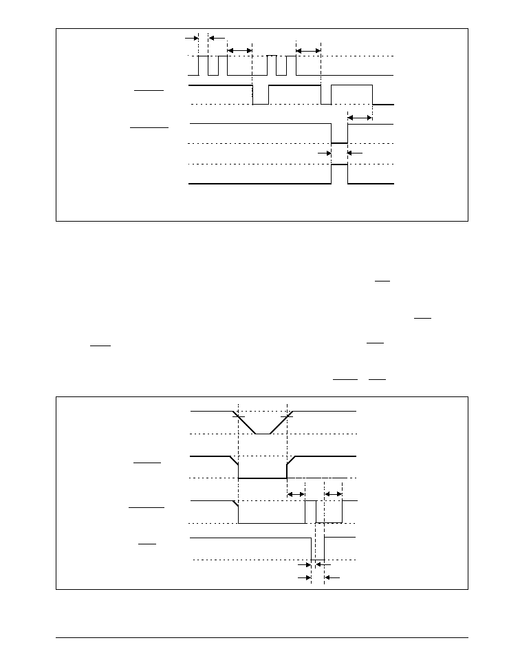
Figure 7A. SP706 RESET Response Time
Figure 7B. Circuit for the SP706 RESET Response
Time
Figure 8. SP708 RESET and RESET Assertion
Figure 9. SP708 RESET and RESET De-Assertion
Figure 10. Circuit for the SP708 RESET and RESET Assertion and De-Assertion
330pF
V
CC
T
A
= +25
o
C
10K
RESET
RESET
330pF
10K
GND
V
CC
330pF
10K
V
CC
T
A
= +25
o
C
V
CC
RESET
RESET
GND
0V
3.2V
RESET
0V
3.2V
RESET
2.8V
0V
0V
2.8V
RESET
RESET
9
Rev. 10-17-00 SP706 +3.0/ +3.3 Low Power Microprocessor Circuits © Copyright 2000 Sipex Corporation
Figure 11. SP708 RESET Output Voltage vs. Supply
Voltage
Figure 12. SP708 RESET Response Time
Figure 13. Circuit for the SP708 RESET Output Voltage vs. Supply Voltage and the RESET Response Time
Figures
GND
RESET
V
CC
330pF
V
CC
10K
0V
0V
RESET
3.6V
V
CC

10
Rev. 10-17-00 SP706 +3.0/ +3.3 Low Power Microprocessor Circuits © Copyright 2000 Sipex Corporation
the reset threshold, an internal timer releases
RESET after 200ms. RESET pulses LOW when-
ever V
CC
dips below the reset threshold, such as
in a brownout condition. When a brownout
condition occurs in the middle of a previously
initiated reset pulse, the pulse continues for at
least another 140ms. During power-down, once
V
CC
falls below the reset threshold, RESET
stays LOW and is guaranteed to be 0.4V or less
until V
CC
drops below 1V.
The active-HIGH RESET output is simply
the complement of the RESET output and is
guaranteed to be valid with V
CC
down to 1.1V.
Some
µ
Ps, such as Intel's 80C51, require an
active-HIGH reset pulse.
Watchdog Timer
The SP706P/R/S/T-SP708R/S/T series watchdog
circuit monitors the
µ
P's activity. If the
µ
P does
not toggle the watchdog input (WDI) within 1.6
seconds and WDI is not tri-stated, WDO goes
LOW. As long as RESET is asserted or the WDI
input is tri-stated, the watchdog timer will stay
cleared and will not count. As soon as RESET
is released and WDI is driven HIGH or LOW,
the timer will start counting. Pulses as short as
50ns can be detected.
Typically, WDO will be connected to the
non-maskable interrupt input (NMI) of a
µ
P.
When V
CC
drops below the reset threshold, WDO
will go LOW independent of the current status
of the watchdog timer. Normally this would
trigger an NMI but RESET goes LOW simulta-
neously, and thus overrides the NMI.
If WDI is left unconnected, WDO can be used as
a low-line output. Since floating WDI disables
the internal timer, WDO goes LOW only when
V
CC
falls below the reset threshold, thus
functioning as a low-line output.
Power-Fail Comparator
The power-fail comparator can be used for
various purposes because its output and
noninverting input are not internally connected.
The inverting input is internally connected to
a 1.25V reference.
FEATURES
The SP706P/R/S/T-SP708R/S/T series provides
four key functions:
1. A reset output during power-up, power-down
and brownout conditions.
2. An independent watchdog output that goes
LOW if the watchdog input has not been toggled
within 1.6 sec.
3. A 1.25V threshold detector for power-fail
warning, low battery detection, or monitoring a
power supply other than +3.3V/+3.0V.
4. An active-LOW manual-reset that allows
RESET to be triggered by a pushbutton switch.
The SP706R/S/T devices are the same as the
SP708R/S/T devices except for the active-HIGH
RESET substitution of the watchdog timer. The
SP706P device is the same as the SP706R de-
vice except an active-HIGH RESET is provided
rather than an active-LOW RESET.
THEORY OF OPERATION
The SP706P/R/S/T-SP708R/S/T series is a mi-
croprocessor (
µ
P) supervisory circuit that moni-
tors the power supplied to digital circuits such
as microprocessors, microcontrollers, or
memory. The series is an ideal solution for
portable, battery-powered equipment that re-
quires power supply monitoring. Implementing
this series will reduce the number of compo-
nents and overall complexity of a system. The
watchdog functions of this product family will
continuously oversee the operational status of a
system. The operational features and benefits of
the SP706P/R/S/T-SP708R/S/T series are de-
scribed, in more detail, below.
RESET Output
A microprocessor's reset input starts the
µ
P
in a known state. The SP706P/R/S/T-SP708R/
S/T series asserts reset during power-up and
prevents code execution errors during power-
down or brownout conditions.
During power-up, once V
CC
reaches 1V, RESET
is a guaranteed logic LOW of 0.4V or less. As
V
CC
rises, RESET stays LOW. When V
CC
rises above
11
Rev. 10-17-00 SP706 +3.0/ +3.3 Low Power Microprocessor Circuits © Copyright 2000 Sipex Corporation
To build an early-warning circuit for power
failure, connect the PFI pin to a voltage divider
as shown in Figure 16. Choose the voltage
divider ratio so that the voltage at PFI falls
below 1.25V just before the +5V regulator drops
out. Use PFO to interrupt the
µ
P so it can prepare
for an orderly power-down.
Manual Reset
The manual-reset input (MR) allows RESET to
be triggered by a pushbutton switch. The switch
is effectively debounced by the 140ms
minimum RESET pulse width. MR is TTL/
CMOS logic compatible, so it can be driven by
an external logic line. MR can be used to force
a watchdog timeout to generate a RESET pulse
in the SP706P/R/S/T-SP708R/S/T series.
Simply connect WDO to MR.
Figure 14. Watchdog Timing Waveforms
Figure 15. Timing Diagrams with WDI Tri-stated. The RESET Output is the Inverse of the RESET Waveform
Shown.
t
RS
RESET*
WDO
0V
WDI
RESET*
0V
+3.3V
0V
0V
t
WD
t
WD
t
WD
t
WP
* externally triggered LOW by MR,
RESET is for the SP813L/813M only
+3.3V
+3.3V
+3.3V
V
CC
RESET
0V
0V
0V
t
RS
t
RS
t
MR
0V
MR*
WDO
V
RT
V
RT
*externally driven LOW
t
MD
+3.3V
+3.3V
+3.3V
+3.3V
12
Rev. 10-17-00 SP706 +3.0/ +3.3 Low Power Microprocessor Circuits © Copyright 2000 Sipex Corporation
Ensuring a Valid RESET Output Down to
V
CC
= 0V
When V
CC
falls below 1V, the RESET output no
longer sinks current, it becomes an open circuit.
High-impedance CMOS logic inputs can drift to
undetermined voltages if left undriven. If a pull-
down resistor is added to the RESET pin, any
stray charge or leakage currents will be shunted
to ground, holding RESET LOW. The resistor
value is not critical. It should be about 100K
,
large enough not to load RESET and small
enough to pull RESET to ground.
Monitoring Voltages Other Than the
Unregulated DC Input
Monitor voltages other than the unregulated DC
by connecting a voltage divider to PFI and
adjusting the ratio appropriately. If required,
add hysteresis by connecting a resistor (with a
value approximately 10 times the sum of the
two resistors in the potential divider network)
between PFI and PFO. A capacitor between PFI
and GND will reduce the power-fail circuit's
sensitivity to high-frequency noise on the
line being monitored. RESET can be used to
monitor voltages other than the +3.3V/+3.0V
V
CC
line. Connect PFO to MR to initiate a
RESET pulse when PFI drops below 1.25V.
Figure 17 shows the SP706R/S/T-SP708R/
S/T series configured to assert RESET when the
+3.3V/+3.0V supply falls below the RESET
threshold, or when the +12V supply falls below
approximately 11V.
Monitoring a Negative Voltage Supply
The power-fail comparator can also monitor a
negative supply rail, shown in Figure 18.
When the negative rail is good (a negative
voltage of large magnitude), PFO is LOW. By
adding the resistors and transistor as shown, a
HIGH PFO triggers RESET. As long as PFO
remains HIGH, the SP706P/R/S/T-SP708R/S/
T series will keep RESET asserted (where
RESET = LOW and RESET = HIGH). Note that
this circuit's accuracy depends on the PFI
threshold tolerance, the V
CC
line, and the resis-
tors.
Interfacing to mPs with Bidirectional
RESET Pins
µ
Ps with bidirectional RESET pins, such as the
Motorola 68HC11 series, can contend with the
RESET output. If, for example, the RESET
PFI
PFO
V
CC
+3.3V/+3.0V
GND
RESET
to
µ
P
MR
+12V
1M
1%
130K
1%
Figure 17. Monitoring Both +3.3V/+3.0V and +12V
Power Supplies
GND
GND
RESET
INTERRUPT
I/O LINE
V
CC
RESET
PFO
PFI
R
2
R
1
Unregulated DC
Power Supply
Regulated +3.3V/+3.0V
Power Supply
V
CC
0.1
µ
F
PFI
µ
P
NMI
WDO
PUSHBUTTON
SWITCH
MR
Figure 16. Typical Operating Circuit
13
Rev. 10-17-00 SP706 +3.0/ +3.3 Low Power Microprocessor Circuits © Copyright 2000 Sipex Corporation
output is driven HIGH and the
µ
P wants to pull
it LOW, indeterminate logic levels may result.
To correct this, connect a 4.7k
resistor
between the RESET output and the
µ
P reset
I/O, as shown if Figure 19. Buffer the
RESET output to other system components.
Negative-Going V
CC
Transients
While issuing resets to the
µ
P during power-up,
power-down, and brownout conditions, these
supervisors are relatively immune to short-
duration negative-going V
CC
transients (glitches).
It is usually undesirable to reset the
µ
P when V
CC
experiences only small glitches.
Figure 20 shows maximum transient dura-
tion vs. reset-comparator overdrive, for which
reset pulses are not generated. The data was gen-
erated using negative-going V
CC
pulses, starting
at 3.3V and ending below the reset threshold by
Figure 18. Monitoring a Negative Voltage Supply
Figure 19. Interfacing to Microprocessors with
Bidirectional RESET I/O for the SP706
PFI
PFO
R
2
R
1
V
CC
+3.3V/+3.0V
GND
PFO
V-
+3.3V
V
TRIP
0V
0V
V
CC
- 1.25
R
1
1.25 - V
TRIP
R
2
V-
=
100k
100k
RESET
to
µ
P
2N3904
, V
TRIP
< 0
V-
MR
0V
+3.3V
MR
the magnitude indicated (reset comparator over-
drive). The graph shows the maximum pulse
width a negative-going V
CC
transient may
typically have without causing a reset pulse to
be issued. As the amplitude of the transient
increases (i.e. goes farther below the reset
threshold), the maximum allowable pulse width
decreases. Typically, a V
CC
transient that goes
100mV below the reset threshold and lasts for
40
µ
s or less will not cause a reset pulse to be
issued. A 100nF bypass capacitor mounted close
to the V
CC
pin provides additional transient
immunity.
Applications
The SP706P/R/S/T-SP708R/S/T series offers
unmatched performance and the lowest power
consumption for these industry standard de-
vices. Refer to Figures 21 and 22 for supply
current performance characteristics rated against
temperature and supply voltages.
V
CC
+3.3V/+3.0V
GND
V
CC
+3.3V/+3.0V
GND
RESET
RESET
4.7K
µ
P
Buffered RESET connects to System Components
14
Rev. 10-17-00 SP706 +3.0/ +3.3 Low Power Microprocessor Circuits © Copyright 2000 Sipex Corporation
Reset Overdrive (mV)
Maximum Transient Duration
100
80
60
40
20
0
10
100
1000
10000
Figure 20. Maximum Transient Duration Without
Causing a Reset Pulse vs. Reset Comparator Overdrive
Figure 21. Supply Current vs. Temperature
Figure 22. Supply Current vs. Supply Voltage
1nF Capacitor
V
OUT
TO GND
Above Line
RESET
Generated
NO
RESET
Generated
14
16
18
20
22
24
26
28
30
2.5
3
3.5
4
4.5
5
5.5
Supply Voltage (V)
19.4
19.5
19.6
19.7
19.8
19.9
20.0
20.1
20.2
-60
-40
-20
0
20
40
60
80
100
Temperature (°C)
Vcc=3.3V
Supply Current (mA)
Supply Current (
µ
A)
Transient Duration (
µ
S)
15
Rev. 10-17-00 SP706 +3.0/ +3.3 Low Power Microprocessor Circuits © Copyright 2000 Sipex Corporation
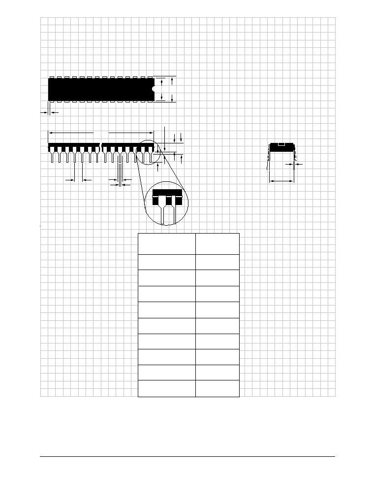
D
ALTERNATE
END PINS
(BOTH ENDS)
D1 = 0.005" min.
(0.127 min.)
E
PACKAGE: PLASTIC
DUALINLINE
(NARROW)
DIMENSIONS (Inches)
Minimum/Maximum
(mm)
A = 0.210" max.
(5.334 max).
E1
C
Ø
L
A2
A1 = 0.015" min.
(0.381min.)
B
B1
e = 0.100 BSC
(2.540 BSC)
e
A
= 0.300 BSC
(7.620 BSC)
A2
B
B1
C
D
E
E1
L
Ø
0.115/0.195
(2.921/4.953)
0.014/0.022
(0.356/0.559)
0.045/0.070
(1.143/1.778)
0.008/0.014
(0.203/0.356)
0.355/0.400
(9.017/10.160)
0.300/0.325
(7.620/8.255)
0.240/0.280
(6.096/7.112)
0.115/0.150
(2.921/3.810)
0
°
/ 15
°
(0
°
/15
°
)
8PIN
16
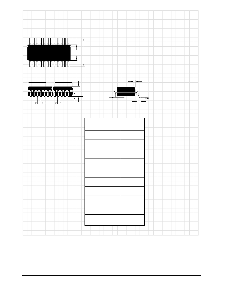
Rev. 10-17-00 SP706 +3.0/ +3.3 Low Power Microprocessor Circuits © Copyright 2000 Sipex Corporation
D
E
H
PACKAGE: PLASTIC
SMALL OUTLINE (SOIC)
(NARROW)
DIMENSIONS (Inches)
Minimum/Maximum
(mm)
8PIN
A
A1
Ø
L
B
e
h x 45
°
A
A1
B
D
E
e
H
h
L
Ø
0.053/0.069
(1.346/1.748)
0.004/0.010
(0.102/0.249
0.014/0.019
(0.35/0.49)
0.189/0.197
(4.80/5.00)
0.150/0.157
(3.802/3.988)
0.050 BSC
(1.270 BSC)
0.228/0.244
(5.801/6.198)
0.010/0.020
(0.254/0.498)
0.016/0.050
(0.406/1.270)
0
°
/8
°
(0
°
/8
°
)
17
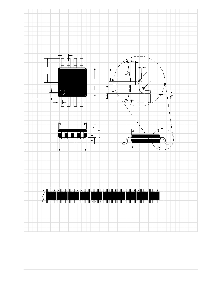
Rev. 10-17-00 SP706 +3.0/ +3.3 Low Power Microprocessor Circuits © Copyright 2000 Sipex Corporation
PACKAGE:
PLASTIC
MICRO SMALL
OUTLINE (
µ
SOIC)
1
0.013
±
0.005
0.0256
BSC
0.118
±
0.004
0.020
2
0.020
0.116
±
0.004
0.034
±
0.004
0.040
±
0.003
0.004
±
0.002
0.118
±
0.004
0.118
±
0.004
0.037
Ref
0.0215
±
0.006
3.0°
±
3°
R .003
12.0°
±
4°
0.006
±
0.006
0.006
±
0.006
0.008
0° - 6°
0.012
±
0.003
0.01
12.0°
±
4°
0.16
±
0.003
0.0965
±
0.003
0.116
±
0.004
50 USOIC devices per tube
All package dimensions are in inches
18
Rev. 10-17-00 SP706 +3.0/ +3.3 Low Power Microprocessor Circuits © Copyright 2000 Sipex Corporation
ORDERING INFORMATION
Model ....................................................................................... Temperature Range ................................................................................ Package
SP706PCP ..................................................................................... 0
°
C to +70
°
C ................................................................................... 8pin PDIP
SP706PCN ..................................................................................... 0
°
C to +70
°
C ................................................................................ 8pin NSOIC
SP706PCU ..................................................................................... 0
°
C to +70
°
C ................................................................................. 8-pin
µ
SOIC
SP706RCP ..................................................................................... 0
°
C to +70
°
C ................................................................................... 8pin PDIP
SP706RCN ..................................................................................... 0
°
C to +70
°
C ................................................................................ 8pin NSOIC
SP706RCU ..................................................................................... 0
°
C to +70
°
C ................................................................................. 8-pin
µ
SOIC
SP706SCP ..................................................................................... 0
°
C to +70
°
C ................................................................................... 8pin PDIP
SP706SCN ..................................................................................... 0
°
C to +70
°
C ................................................................................ 8pin NSOIC
SP706SCU ..................................................................................... 0
°
C to +70
°
C ................................................................................. 8-pin
µ
SOIC
SP706TCP ..................................................................................... 0
°
C to +70
°
C ................................................................................... 8pin PDIP
SP706TCN ..................................................................................... 0
°
C to +70
°
C ................................................................................ 8pin NSOIC
SP706TCU ..................................................................................... 0
°
C to +70
°
C ................................................................................. 8-pin
µ
SOIC
SP706PEP ................................................................................... -40
°
C to +85
°
C ................................................................................. 8pin PDIP
SP706PEN ................................................................................... -40
°
C to +85
°
C .............................................................................. 8pin NSOIC
SP706PEU ................................................................................... -40
°
C to +85
°
C ............................................................................... 8-pin
µ
SOIC
SP706REP ................................................................................... -40
°
C to +85
°
C ................................................................................. 8pin PDIP
SP706REN ................................................................................... -40
°
C to +85
°
C .............................................................................. 8pin NSOIC
SP706REU ................................................................................... -40
°
C to +85
°
C ............................................................................... 8-pin
µ
SOIC
SP706SEP ................................................................................... -40
°
C to +85
°
C ................................................................................. 8pin PDIP
SP706SEN ................................................................................... -40
°
C to +85
°
C .............................................................................. 8pin NSOIC
SP706SEU ................................................................................... -40
°
C to +85
°
C ............................................................................... 8-pin
µ
SOIC
SP706TEP ................................................................................... -40
°
C to +85
°
C ................................................................................. 8pin PDIP
SP706TEN ................................................................................... -40
°
C to +85
°
C .............................................................................. 8pin NSOIC
SP706TEU ................................................................................... -40
°
C to +85
°
C ............................................................................... 8-pin
µ
SOIC
SP708RCP ..................................................................................... 0
°
C to +70
°
C ................................................................................... 8pin PDIP
SP708RCN ..................................................................................... 0
°
C to +70
°
C ................................................................................ 8pin NSOIC
SP708RCU ..................................................................................... 0
°
C to +70
°
C ................................................................................. 8-pin
µ
SOIC
SP708SCP ..................................................................................... 0
°
C to +70
°
C ................................................................................... 8pin PDIP
SP708SCN ..................................................................................... 0
°
C to +70
°
C ................................................................................ 8pin NSOIC
SP708SCU ..................................................................................... 0
°
C to +70
°
C ................................................................................. 8-pin
µ
SOIC
SP708TCP ..................................................................................... 0
°
C to +70
°
C ................................................................................... 8pin PDIP
SP708TCN ..................................................................................... 0
°
C to +70
°
C ................................................................................ 8pin NSOIC
SP708TCU ..................................................................................... 0
°
C to +70
°
C ................................................................................. 8-pin
µ
SOIC
SP708REP ................................................................................... -40
°
C to +85
°
C ................................................................................. 8pin PDIP
SP708REN ................................................................................... -40
°
C to +85
°
C .............................................................................. 8pin NSOIC
SP708REU ................................................................................... -40
°
C to +85
°
C ............................................................................... 8-pin
µ
SOIC
SP708SEP ................................................................................... -40
°
C to +85
°
C ................................................................................. 8pin PDIP
SP708SEN ................................................................................... -40
°
C to +85
°
C .............................................................................. 8pin NSOIC
SP708SEU ................................................................................... -40
°
C to +85
°
C ............................................................................... 8-pin
µ
SOIC
SP708TEP ................................................................................... -40
°
C to +85
°
C ................................................................................. 8pin PDIP
SP708TEN ................................................................................... -40
°
C to +85
°
C .............................................................................. 8pin NSOIC
SP708TEU ................................................................................... -40
°
C to +85
°
C ............................................................................... 8-pin
µ
SOIC
Please consult the factory for pricing and availability on a Tape-On-Reel option.
Corporation
SIGNAL PROCESSING EXCELLENCE
Sipex Corporation reserves the right to make changes to any products described herein. Sipex does not assume any liability arising out of the
application or use of any product or circuit described herein; neither does it convey any license under its patent rights nor the rights of others.
Sipex Corporation
Headquarters and
Sales Office
22 Linnell Circle
Billerica, MA 01821
TEL: (978) 667-8700
FAX: (978) 670-9001
e-mail: sales@sipex.com
Sales Office
233 South Hillview Drive
Milpitas, CA 95035
TEL: (408) 934-7500
FAX: (408) 935-7600