 | ÐлекÑÑоннÑй компоненÑ: SP7648ER | СкаÑаÑÑ:  PDF PDF  ZIP ZIP |
DATASHEET SEARCH SITE | WWW.ALLDATASHEET.COM
1
Date: 7/20/05
SP7648 Ultra-low Quiescent Current, High Efficiency Boost Regulator © Copyright 2005 Sipex Corporation
SP7648
FEATURES
True Shutdown
700mA Output Current at 3.3V Input; 4.2V
output
92% Efficiency from 2.7V
IN
to 3.3V
OUT
Wide Input Voltage Range: 2.7V to 4.5V
5V Fixed or Adjustable Output
0.3
Switch
Integrated Synchronous Rectifier:0.3
Anti-Ringing Switch Technology
Programmable Inductor Peak Current
Logic Shutdown Control
Low 0.8V or 0.288V Reference Voltage
Small 10 pin DFN or MSOP Package
Low Reference High Efficiency Boost Regulator
APPLICATIONS
LED Driver
Camera Flash
Handheld Portable Devices
DESCRIPTION
The SP7648 is an ultra-low quiescent current, high efficiency step-up DC-DC converter ideal for
single cell Li-Ion or dual cell alkaline battery applications to drive various LEDs. The SP7648
combines low quiescent current and excellent light-load efficiency of PFM control. The SP7648
features synchronous rectification, a 0.3
charging switch, an anti-ringing inductor switch, under-
voltage lockout and programmable inductor peak current. The device can be shut down by a
1nA active LOW shutdown pin. A very low 0.288V reference voltage is optimized for driving a
constant current load.
®
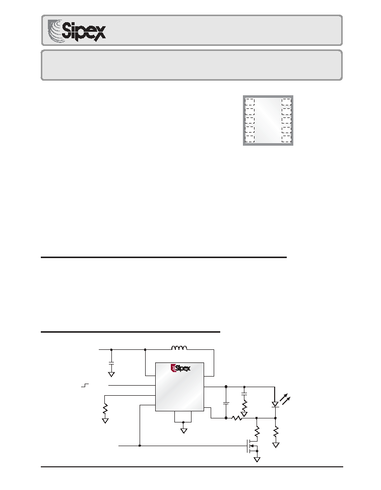
TYPICAL APPLICATION CIRCUIT
Now Available in Lead Free Packaging
SP7648
10 Pin DFN
10
9
8
7
6
1
2
3
4
5
V
OUT
LX
P
GND
GND
FB
FLASH
SHDN
NC (Test)
R
LIM
V
BATT
Preliminary
®
4.7
µ
H
V
IN
SP7648
V
BATT
FLASH
FB
LX
V
OUT
NC
1.0K
ON/OFF
10
µ
F
SHDN
GND
10
µ
F
P
GND
0.33
R
LIM
(2.7 - 4.5V)
FLASH
470pF
R
LIM
1K
R
1
R
2
Q
1
D
1
2
Date: 7/20/05
SP7648 Ultra-low Quiescent Current, High Efficiency Boost Regulator © Copyright 2005 Sipex Corporation
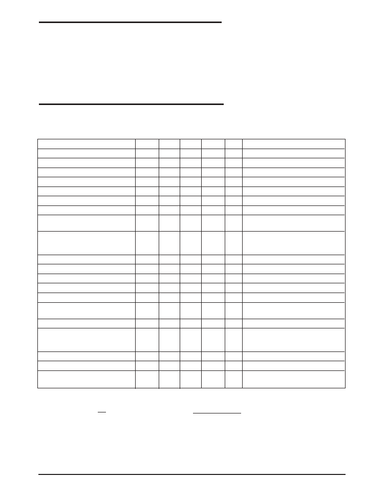
LX, Vo, V
BATT
, FLASHOUT, FB to GND pin ...................... -0.3 to 6.0V
SHDN, FLASH ..................................................... -0.3V to V
BATT
+1.0V
Vo, GND, LX Current ....................................................................... 2A
Reverse V
BATT
Current .............................................................. 220mA
Forward V
BATT
Current .............................................................. 500mA
Storage Temperature .................................................. -65
°
C to 150
°
C
PARAMETER
MIN
TYP
MAX
UNITS
CONDITIONS
Input Voltage Operating Range, V
BATT
2.7
-
4.5
V
After Startup
Output Voltage Range, V
OUT
2.7
-
5.5
V
Under Voltage Lock-out/UVLO
0.5
0.61
0.7
V
Output Voltage, V
O
4.6
5.0
5.4
V
Internal Feedback Divider
Shutdown Current into V
O,
I
SDO
-
1
500
nA
V
SHDN
= ZeroV
Shutdown Current into V
BATT,
I
SDB
-
250
750
nA
V
SHDN
= ZeroV, V
BATT
= 2.7V
Efficiency
92
-
%
-
V
BATT
= 2.7V, I
OUT
= 200mA, R
LIM
= 2k
Inductor Peak Current Limit, I
PK
650
800
1000
mA
R
LIM
= 2k
, I
PK
= 1600/R
LIM
1600
mA
R
LIM
= 1k
, I
PK
= 1600/R
LIM
Output Current (Note 2)
-
800
-
mA
-
V
BATT
= 2.7V, R
LIM
=1k
-
400
-
mA
-
V
BATT
= 2.7V, R
LIM
=2k
-
200
-
mA
-
V
BATT
= 2.7V, R
LIM
= 4k
Minimum Off-Time Constant K
OFF
0.5
1.0
1.5
V*
µ
s
K
OFF
T
OFF
(V
OUT
- V
BATT
)
Maximum On-Time Constant K
ON
2.0
3.5
5.0
V*
µ
s
K
ON
T
ON
(V
BATT
)
Enable Valid to Output Stable (Note 3)
-
300
500
µ
s
-
I
LOAD
= 1mA
NMOS
Switch Resistance
-
0.30
0.6
I
NMOS
= 100mA
PMOS
Switch Resistance
-
0.30
0.6
I
PMOS
= 100mA
FB Set Voltage, V
FB
0.76
0.8
0.84
V
External feedback Flash = 0
0.266
0.288
0.310
V
External feedback Flash = 1
FB Input Current
-
1
100
nA
V
FB
=1.3V
SHDN Input Voltage (Note 1)
V
IL
-
-
0.5
V
V
BATT
= 2.7V
V
IH
2.0
-
-
V
BATT
= 2.7V
SHDN Input Current
-
1
100
nA
LX Pin Leakage
-
-
3
µ
A
-
FLASH Threshold V
IL
-
-
0.4
V
V
IH
1.0
-
-
V
ELECTRICAL SPECIFICATIONS
V
BATT
=V
SHDN
= 3.6V, V
FB
=ZeroV, I
LOAD
= 0mA, T
AMB
= -40
°
C to +85
°
C, V
OUT
= 5.0V, typical values at 27
°
C unless
otherwise noted. The
denotes the specifications which apply over full operating temperature range -40ºC to +85
°
C, unless
otherwise specified.
Operating Temperature ................................................ -40
°
C to +85
°
C
ESD Rating ........................................................................ 1.5kV HBM
These are stress ratings only and functional operation of the device at
these ratings or any other above those indicated in the operation sections
of the specifications below is not implied. Exposure to absolute maximum
rating conditions for extended periods of time may affect reliability.
ABSOLUTE MAXIMUM RATINGS
Note 1: SHDN must transition faster than 1V/100mS for proper operation.
Note 2: Output Current I =
{
VIN
}
X Efficiency x
{
Inductor Peak Current - Inductor Ripple Current
}
VOUT
2
Note 3: Guaranteed by Design.
3
Date: 7/20/05
SP7648 Ultra-low Quiescent Current, High Efficiency Boost Regulator © Copyright 2005 Sipex Corporation
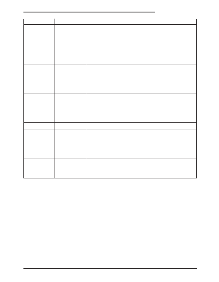
PIN DESCRIPTION
PIN NUMBER
PIN NAME
DESCRIPTION
1
V
BATT
Battery Voltage. The startup circuitry is powered by this pin. Battery
Voltage is used to calculate switch off time: T
OFF
= K
OFF
/ (V
OUT
-
V
BATT
). When the battery voltage drops below 0.61V the SP7648
goes into an undervoltage lockout mode (UVLO), where the part is shut
down.
2
FLASH
Reference Control Input. Internal Reference defaults to 0.8V if FLASH
= LOW and 0.288V if FLASH = HIGH.
3
NC (Test)
No connection. This pin is bonded out for test purposes only and
must be left floating in all applications.
4
R
LIM
Current Limit Resistor. By connecting a resistor R
LIM
from this pin to
ground the inductor peak current is set by I
PEAK
=1600/R
LIM
. The range
for R
LIM
is 9k
(for 180mA) to 1.K
(for 1.6A).
5
SHDN
Shutdown Not. Tie this pin high to V
BATT,
for normal operation. Pull
this pin to ground to disable all circuitry inside the chip.
6
FB
Feedback. Connect this pin to GND for fixed +5V operation. Connect
this pin to a resistor voltage divider between V
OUT
and GND for
adjustable output operation.
7
GND
Ground. Connect to ground plane.
8
PGND
Power Ground. The inductor charging current flows out of this pin.
9
LX
Inductor Switching Node. Connect one terminal of the inductor to the
positive terminal of the battery. Connect the second terminal of the
inductor to this pin. The inductor charging current flows into LX,
through the internal charging N-channel FET, and out the PGND pin.
10
V
OUT
Output Voltage. The inductor current flows out of this pin during
switch off-time. It is also used as the internal regulator voltage supply.
Connect this pin to the positive terminal of the output capacitor.
4
Date: 7/20/05
SP7648 Ultra-low Quiescent Current, High Efficiency Boost Regulator © Copyright 2005 Sipex Corporation
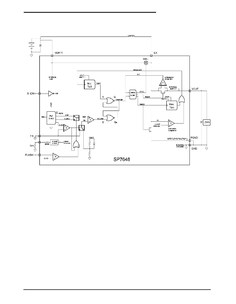
FUNCTIONAL DIAGRAM

5
Date: 7/20/05
SP7648 Ultra-low Quiescent Current, High Efficiency Boost Regulator © Copyright 2005 Sipex Corporation
_________________________DETAILED
DESCRIPTION
The SP7648 is a step-up DC-DC converter
with an input voltage operation range from
2.7V to 4.7V. In addition to the main 0.3
internal NMOSFET switch the SP7648 has
an internal synchronous rectifier, thereby
increasing efficiency and reducing the space
and cost of an external diode. An internal
inductive-damping switch significantly re-
duces inductive ringing for low noise-high
efficiency operation. If the supply voltage
drops below 0.61V the SP7648 goes into
under voltage lockout, thus opening both
internal switches. The inductor peak current
is externally programmable to allow for a
range of inductor values.
__________________________ CIRCUIT
LAYOUT
Printed circuit board layout is a critical part of
a power supply design. Poor designs can
result in excessive EMI on the feedback
paths and on the ground planes with applica-
tions involving high switching frequencies
and large peak currents. Excessive EMI can
result in instability or regulation errors. All
power components should be placed on the
PC board as closely as possible with the
traces kept short, direct, and wide (>50mils
or 1.25mm). Extra copper on the PC board
should be integrated into ground as a pseudo-
ground plane. On a multilayer PC board,
route the star ground using component-side
copper fill, then connect it to the internal
ground plane using vias. For the SP7648
THEORY OF OPERATION
devices, the inductor and input & output filter
capacitors should be soldered with their
ground pins as close together as possible in
a star-ground configuration. The V
OUT
pin
must be bypassed directly to ground as
close to the SP7648 devices as possible
(within 0.2in or 5mm). The DC-DC converter
and any digital circuitry should be placed on
the opposite corner of the PC board as far
away from sensitive RF and analog input
stages. Noisy traces, such as from the LX
pin, should be kept away from the voltage-
feedback V
FB
node and separated from it
using grounded copper to minimize EMI.
See the SP7648EB Evaluation Board
Manual for PC Board Layout design details.
________________ CONTROL SCHEME
A minimum off-time, current limited pulse
frequency modulation (PFM) control scheme
combines the high output power and effi-
ciency of a pulse width modulation (PWM)
device with the ultra low quiescent current of
the traditional PFM. At low to moderate
output loads the PFM control provides higher
efficiency than traditional PWM converters
are capable of delivering. At these loads the
switching frequency is determined by a mini-
mum off-time (T
OFF
, MIN) and a maximum
on-time (T
ON
, MAX) where:
T
OFF
< K
OFF
/ (V
OUT
- V
BATT
)
T
ON
> K
ON
/ V
BATT
K
OFF
= 1.0V
µ
s
K
ON
= 3.5 V
µ
s
6
Date: 7/20/05
SP7648 Ultra-low Quiescent Current, High Efficiency Boost Regulator © Copyright 2005 Sipex Corporation
THEORY OF OPERATION
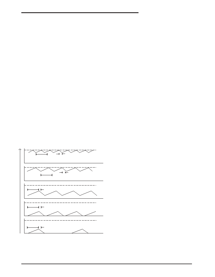
Figure 1. Inductor Current vs. Load
At light loads (as shown in plot A in Figure 1)
the charge cycle will last the maximum value
for
t
ON
: For a 3V battery this would be as
follows: T
ON
= K
ON
/ V
BATT
= 3.5V
µ
S/ 3V =
1.17
µ
S. The current built up in the coil during
the charge cycle gets fully discharged in the
discontinuous conduction mode (DCM).
When the current in the coil has reached
zero, the synchronous rectifier switch is
opened and the voltage across the coil (from
V
BATT
to LX) is shorted internally to eliminate
inductive ringing. With increasing load (as
shown in plot B in Figure 1) this inductor
damping time becomes shorter, because
the output will quickly drop below its regula-
tion point due to heavier load. If the load
current increases further, the SP7648 en-
ters continuous conduction mode (CCM)
where there is always current flowing in the
inductor. The charge time remains at maxi-
mum T
ON
as long as the inductor peak
current limit is not reached as shown in plot
C in Figure 1. The inductor peak current limit
can be programmed by tying a resistor R
LIM
from the R
LIM
pin to ground where:
I
PEAK
= 1600 / R
LIM
When the peak current limit is reached the
charge time is short-cycled. In plot D of
Figure 1, the switch current reaches the
peak current limit during the charge period
which ends the charge cycle and starts the
discharge cycle. However, full load is not yet
achieved because at the end of the mini-
mum discharge time the output was still
within regulation. Maximum load is reached
when this discharge time has shrunk to the
minimum allowed value T
OFF
as shown in
Plot E of Figure 1.
_____________________ COMPONENT
SELECTION
Selection of capacitors for SP7648 power
supply circuits can be made through the use
of the Component Selection Table. Capaci-
tor equivalent series resistance (ESR) in the
range of 0.2 to 0.3
is a requirement for
obtaining sufficient output voltage ripple for
the SP7648 to properly regulate under its
load. For example, in the SP7648 applica-
tion circuit a 10
µ
F, 10V, X5R, surface mount
ceramic output filter capacitor is used.
Ceramic capacitors have an ESR too low to
produce enough output ripple for the SP7648
to regulate the output; therefore, a 0.33
resistor is added in series with the 10
µ
F
capacitor at the V
OUT
pin. Designers should
select input and output capacitors with a
rating exceeding the inductor current ripple,
which is typically set by the inductor value
and the K
ON
value as given in the following
relationship:
I
L(RIPPLE)
= K
ON
/L, where K
ON
= 3.5V*
µ
S
Inductor Current vs. Load
Ton Max.
Toff Min.
E. Iripple=Toff* (Vo
- Vi)/L
llim
llim
llim
llim
llim
Ton Max.
Ton Max.
Ton Max.
Ton Max.
Toff Min.
Toff Min.
Toff Min.
Toff Min.
D. Toff*= (Vo
- Vi)/L<Iripple<Ton*Vi/L
C. Iripple=Ton*Vi/L
B. Iripple=Ton*Vi/L
A. Iripple=Ton*Vi/L
E
D
C
B
A
7
Date: 7/20/05
SP7648 Ultra-low Quiescent Current, High Efficiency Boost Regulator © Copyright 2005 Sipex Corporation
For the example, a 10
µ
H inductor would
have an inductor current ripple of 350mA,
while a 4.7
µ
H inductor would have an in-
ductor current ripple value of 740mA. Do not
allow tantalum capacitors to exceed their
ripple-current ratings. An input filter capaci-
tor can reduce peak currents drawn from
the battery and improve efficiency. For
most applications, use the same capacitor
for the input and output.
Low-ESR tantalum capacitors are accept-
able provided they meet the ESR require-
ment of 0.2
to 0.3
. In selecting an
inductor, the saturation current specified for
the inductor needs to be greater than the
SP7648 peak current to avoid saturating
the inductor, which would result in a loss of
efficiency and could damage the inductor.
The SP7648 evaluation board uses a Wurth
4.7
µ
H inductor with an I
SAT
value of 1.7A
and a DCR of 0.065
, which handles the
I
PEAK
of 1.6A of the SP7648 and will deliver
high efficiencies. Other inductors could be
selected provided their I
SAT
is greater than
the I
PEAK
of the SP7648.
THEORY OF OPERATION
______________ V
OUT
PROGRAMMING
The SP7648 can be programmed as either
a voltage source or a current source. To
program the SP7648 as voltage source, the
SP7648 requires 2 feedback resistors R1 &
R2 to control the output voltage. To set V
OUT
in the voltage mode, use the equation:
R1 = [(V
OUT
/0.8)-1] * R2, where flash < 0.4V,
R1 = [(V
OUT
/0.288)-1] * R2, where flash > 1.0V
_______________________ USING THE
R
LIM
FUNCTION
The peak inductor current, I
PEAK
, is pro-
grammed externally by the R
LIM
resistor
connected between the R
LIM
pin and GND.
The peak inductor current is defined by:
I
PEAK
= 1600/R
LIM
The saturation current specified for the in-
ductor needs to be greater than the peak
INDUCTORS - SURFACE MOUNT
Inductor Specification
Inductance
Manufacturer/Part No.
Series R
Isat
Size LxWxH
Inductor Type
Manufacturer
(uH)
ohms
(A)
(mm)
Website
4.7
Wurth Elektronik 744042004
0.070
1.70
4.8x4.8x1.8
Shielded Ferrite Core
www.we-online.de
4.7
TDK SLF6025T-4R7M1R5-PF
0.031
1.50
6.0x6.0x2.5
Shielded Ferrite Core
www.tdk.com
4.7
Coilcraft MSS6122-4R7MX
0.065
1.85
6.1x6.1x2.2
Shielded Ferrite Core
www.coilcraft.com
6.8
Wurth Elektronik 744042006
0.080
1.50
4.8x4.8x1.8
Shielded Ferrite Core
www.we-online.de
6.8
TDK SLF6025T-6R8M1R3-PF
0.044
1.30
6.0x6.0x2.5
Shielded Ferrite Core
www.tdk.com
6.8
Coilcraft MSS6122-6R8MX
0.100
1.45
6.1x6.1x2.2
Shielded Ferrite Core
www.coilcraft.com
CAPACITORS - SURFACE MOUNT
Capacitor Specification
Capacitance
Manufacturer/Part No.
ESR
Ripple Current
Size LxWxH
Voltage
Capacitor
Manufacturer
(uF)
ohms (max)
10C Rise (A)
(mm)
(V)
Type
Website
10
TDK C2012X5R0J106M
0.020
1.70
2.0x1.2x1.35
6.3
X5R Ceramic
www.tdk.com
10
Murata GRM21BR60J106KE19L
0.020
1.70
2.0x1.2x1.35
6.3
X5R Ceramic
www.murata.com
MOSFETS - SURFACE MOUNT
MOSFET Specification
MOSFET
Manufacturer/Part No.
RDS(on)
Id
Package
Manufacturer
type
ohms
(A)
Size
Website
NMOS
Vishay Si1400DL
0.190
1.70
SC70-6
www.vishay.com
NMOS
Fairchild FDN337N
0.070
2.20
SOT23-3
www.fairchildsemi.com
RESISTORS - LOW VALUE SURFACE MOUNT
Resistor Specification
Resistor
Manufacturer/Part No.
Resistance
Pd
Package
Manufacturer
Ref. Des.
ohms
(W)
Size
Website
Rc, R2
Vishay CRCW0603R33F
0.33
0.10
0603
www.vishay.com
Rc, R2
Vishay CRCW0603R22F
0.22
0.10
0603
www.vishay.com
Note: Components highlighted in bold are those used on the SP7648EB Evaluation Board.
30V, Vgs = 2.5V, Pd = 0.5W
MOSFET
Specifications
20V, Vgs = 2.5V, Pd = 0.5W
Resistor
Specifications
Thick Film 1% or 5%
Thick Film 1% or 5%
Table 1: Component Selection

8
Date: 7/20/05
SP7648 Ultra-low Quiescent Current, High Efficiency Boost Regulator © Copyright 2005 Sipex Corporation
current to avoid saturating the inductor,
which would result in a loss in efficiency and
could damage the inductor. The SP7648
evaluation board uses a R
LIM
value of 1K
for an I
PEAK
= 1.6A to allow the circuit to
deliver up to 700mA for V
IN
= 3.3V and V
OUT
= 4.2V. Other values could be selected using
the above relationships.
_________________USING THE FLASH
CONTROL PIN
The SP7648 will regulate the output by the
equations above depending on the state of
the FLASH pin. When the FLASH pin is low
(<0.4V), the internal reference voltage is
defined as 0.8V. When the FLASH pin is
high (>0.4V), the internal reference voltage
is defined as 0.288V. This allows the use of
smaller values for the sense resistor for
current regulation mode. This improves effi-
ciency and reduces the physical size of the
sense resistor. An external MOSFET switch
can be used to change the sense resistor
when changing to the Flash Mode.
________________ HIGH BRIGHTNESS
WHITE LED
For the high brightness LumiLED white LED
application, the SP7648 is generally pro-
grammed as a current source. The bias
resistors R1 and R2 are used to set the
operating current of the white LED with the
equation:
R = V
FB
/I
F
where V
FB
is 0.8V in torch mode and 0.288V
in flash mode, I
F
is the operating current of
THEORY OF OPERATION
the LED. To set the operating current to be
about 200mA in torch mode, the flash pin is
forced low, R2 is selected as 0.8V/ 0.2 = 4
,
as shown in the typical application circuit. To
set the operating current to 700mA in flash
mode, the flash pin is forced high, R is
selected as 0.288V/0.41
= 700mA. In real-
ity R in Flash includes the series MOSFET
R
DSON
and the parallel combination of R
2
=
4
shown by the formula:
R in Flash =
{R
1
X (R
2
+ Q
1
R
DSON
)}
{R
1
+ R
2
+ Q
1
R
DSON
}
If the SP7648 is powered up before the LED
is plugged in, the circuit will bring the feed-
back pin to ZeroV and the SP7648 has a
feature to set the output voltage to be 5V.
Once the LED is plugged in, the feedback
pin will go up to 0.8V in torch mode or 0.288V
in flash mode and begin to regulate. The
output voltage will go from 5V to V
F
+V
FB
,
where V
F
is the forward voltage of the LED.
When the LED is open, the feedback pin
voltage will go to ZeroV and the output
voltage will go to 5V which will protect the
part from overvoltage at the output.
One approach to control LED brightness is
to apply a PWM signal to the SHDN input of
the SP7648. In this case, the output current
will be equal to the product of V
REF
/R1 and
the average duty cycle at the SHDN pin. An
optional 10K
potentiometer may also be
used for dimming the LED current by varying
the potentiometer between low brightness
and full brightness.
If the FB pin is pulled below 150mV the
output will default to 5V defined by an inter-
nal resistor divider.
9
Date: 7/20/05
SP7648 Ultra-low Quiescent Current, High Efficiency Boost Regulator © Copyright 2005 Sipex Corporation
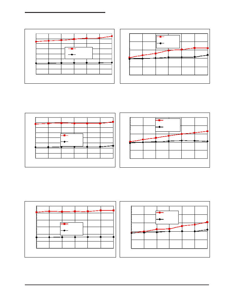
TYPICAL PERFORMANCE CHARACTERISTICS
SP7648 for Luxeon I
0
100
200
300
400
500
600
700
800
3.0
3.2
3.4
3.6
3.8
4.0
4.2
Vin (V)
Output current (mA)
Flash Mode,
Vf=3.6V
Torch Mode,
Vf=3.2V
SP7648 for Luxeon I
50
60
70
80
90
100
3.0
3.2
3.4
3.6
3.8
4.0
4.2
Vin (V)
Efficiency (%)
Flash Mode,
Vf=3.6V
Torch Mode,
Vf=3.2V
SP7648 for AOT(2015HPW1915B)
0
100
200
300
400
500
600
700
800
3.0
3.2
3.4
3.6
3.8
4.0
4.2
Vin (V)
Output current (mA)
Flash Mode,
Vf=3.9V
Torch Mode,
Vf=3.3V
SP7648 for AOT(2015HPW1915B)
50
60
70
80
90
100
3.0
3.2
3.4
3.6
3.8
4.0
4.2
Vin (V)
Efficiency (%)
Flash Mode,
Vf=3.9V
Torch
Mode,Vf=3.3V
SP7648 for AOT(6060HPW0305BD)
0
100
200
300
400
500
600
3.0
3.2
3.4
3.6
3.8
4.0
4.2
Vin (V)
Output current (mA)
Flash Mode,
Vf=4.2V
Torch Mode,
Vf=3.5V
SP7648 for AOT(6060HPW0305BD)
50
60
70
80
90
100
3.0
3.2
3.4
3.6
3.8
4.0
4.2
Vin (V)
Efficiency (%)
Flash Mode,
Vf=4.2V
Torch Mode,
Vf=3.5V
10
Date: 7/20/05
SP7648 Ultra-low Quiescent Current, High Efficiency Boost Regulator © Copyright 2005 Sipex Corporation
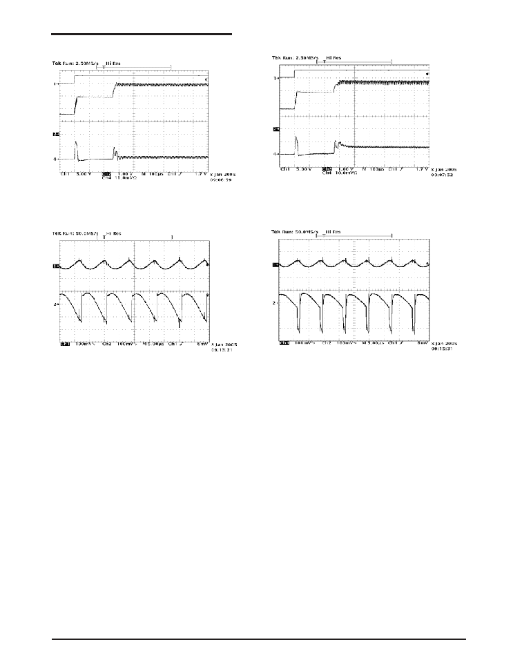
Startup 700mA Flash, Vin = 3.6V, Vout = 3.65V
Startup 200mA Torch, Vin = 3.6V, Vout = 3.9V
Ripple 700mA Flash, Vin = 3.6V, Vout = 3.65V
Ripple 200mA Torch, Vin = 3.6V, Vout = 3.9V
TYPICAL PERFORMANCE CHARACTERISTICS
Ch1 = SHDN (5V/div)
Ch2 = Vout (1V/div)
Ch4 = Iin (1A/div)
Ch1 = Vin (AC)
100mV/div
Ch2 = Vout (AC)
100mV/div
11
Date: 7/20/05
SP7648 Ultra-low Quiescent Current, High Efficiency Boost Regulator © Copyright 2005 Sipex Corporation
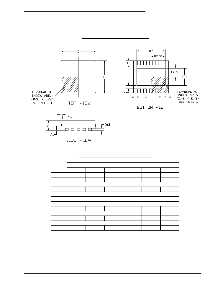
PACKAGE: 10 PIN DFN
MINIMUM
NOMINAL MAXIMUM MINIMUM
NOMINAL MAXIMUM
A
0.80
0.90
1.00
0.032
0.035
0.039
A1
0.00
0.02
0.05
0.000
0.001
0.002
A3
b
0.18
0.25
0.30
0.007
0.010
0.012
e
D
E
D2
2.20
--
2.70
0.087
--
0.106
E2
1.40
--
1.75
0.055
--
0.069
L
0.30
0.40
0.50
0.012
0.016
0.020
K
0.20
--
--
0.008
--
--
0
o
--
14
o
0
o
--
14
o
N
ND
NOTE 1: PIN #1 INDICATOR MUST BE WITHIN THIS AREA AND CAN BE ANY SHAPE
(CONVERT UNIT 1MM = 0.0394INCH)
0.20 REF
10
0.008 REF
10
10-PIN 3X3MM DFN PACKAGE OUTLINE
JEDEC DOCUMENT MO-229 VARIATION VEED-5
0.50 BSC
3.00 BSC
DIMENSIONS IN MILLIMETERS
SYMBOL
(CONTROLLING UNIT)
DIMENSIONS IN INCHES
5
0.020 BSC
0.118 BSC
0.118 BSC
5
3.00 BSC
12
Date: 7/20/05
SP7648 Ultra-low Quiescent Current, High Efficiency Boost Regulator © Copyright 2005 Sipex Corporation
Corporation
ANALOG EXCELLENCE
Sipex Corporation reserves the right to make changes to any products described herein. Sipex does not assume any liability arising out of the
application or use of any product or circuit described herein; neither does it convey any license under its patent rights nor the rights of others.
Sipex Corporation
Headquarters and
Sales Office
233 South Hillview Drive
Milpitas, CA 95035
TEL: (408) 934-7500
FAX: (408) 935-7600
Sales Office
22 Linnell Circle
Billerica, MA 01821
TEL: (978) 667-8700
FAX: (978) 670-9001
e-mail: sales@sipex.com
Part Number
Operating Temperature Range
Package Type
SP7648ER .................................................. -40
°
C to +85
°
C ........................................................... 10 Pin DFN
SP7648ER/TR ............................................ -40
°
C to +85
°
C .......................................................... 10 Pin DFN
SP7648EU .................................................. -40
°
C to +85
°
C ........................................................ 10 Pin MSOP
SP7648EU/TR ............................................ -40
°
C to +85
°
C ....................................................... 10 Pin MSOP
ORDERING INFORMATION
Available in lead free packaging. To order add "-L" suffix to part number.
Example: SP7648ER/TR = standard; SP7648ER-L/TR = lead free
/TR = Tape and Reel
Pack quantity is 2,500 for DFN and MSOP.
CLICK HERE TO ORDER SAMPLES