SP7683 Four Channel Charge Pump LED Driver
1
Date: 12/21/04
SP7683 Four Channel Charge Pump LED Driver © Copyright 2004 Sipex Corporation
SP7683
FEATURES
2.7V to 5.5V Input Voltage Range
Up to 4 LEDS with matching currents
LEDs can be Driven from the Charge
Pump Output
1X and 1.5X Mode Charge Pump
High Efficiency Operation
1.2 MHz Switching Frequency
Programable LED Drive Capabliity
PWM Dimming Control
Low 0.5µA Shutdown Current
Soft-Start Limits Inrush Current
Output Overvoltage Protection
Thermal Shutdown Protection
QFN (4mm x 4mm) package
Four Channel Charge Pump Regulator LED Driver
APPLICATIONS
Smart Phones
Cell Phones
PDA's
Digital Cameras
MP3 Players
Other Portables
The SP7683 is high efficiency Charge Pump which regulates up to four white LEDs with matching
current. Based on the supply headroom available for the four precision current sinks, SP7683
automatically switches between 1X and 1.5X modes. The part powers up in 1X mode, with low
quiescent current of 70uA (typ) and remains in 1X mode as long as the LED current has not
decreased by more than 0.5%. If the current decreases, then it switches into 1.5X mode where
it regulates the lowest of the LED cathode voltages to 0.1V. Other features include soft-start, over
current protection, overvoltage protection and thermal shutdown at 140°C. Offered in 4X4 16 pin
QFN.
®
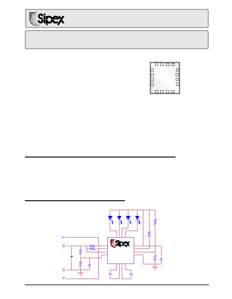
TYPICAL APPLICATION SCHEMATIC
Now Available in Lead Free Packaging
Advanced
DESCRIPTION
R1
50k - 200k
GND
R3
100k
LED_EN
U1
SP7683
R5
10k
R4
270k
R9
100k
C1
1uF
C5
1uF
C4
1uF
C2
1uF
R2
1M
D1
D2
EN
Vin
D3
D4
C3
0.1uF
R10
100k
®
®
SP7683
1
2
7
4
6
5
3
9
8
12
13
10
11
14
15 16
R
SE
T
C1P
GND
C2P
C1N
SP7683
4x4 mm
16 Pin QFN
V
OUT
8
7
6
5
4
3
2
1
FB
EN/ PWM
C2N
LED1
LED2
On/Off
LED3
LED4
12
11
10
9
16
15
14
13
I
SET
V
MODE
V
IN

2
Date: 12/21/04
SP7683 Four Channel Charge Pump LED Driver © Copyright 2004 Sipex Corporation
ELECTRICAL CHARACTERISTICS
Unless otherwise specified: V
IN
= 3.6V, MODE = 0V, ILX = 0mA, T
A
= -40°C to +85°C, typical values at 27º unless
otherwise noted.
These are stress ratings only and functional operation of the device at these ratings or any other above those indicated in the operation sections of the
specifications below is not implied. Exposure to absolute maximum rating conditions for extended periods of time may affect reliability.
I
SET
Voltage to GND.....................................................0.5V
IN, OUT, EN1, EN2 to GND................................-0.3V to 6V
SET, LED1, LED2, LED3, LED4 to GND -0.3V to IN+0.3V
C1N, C2N to GND...........................................-0.3 to IN+1V
C1P, C2P to GND - 0.3V to greater than IN+1 or OUT+1V
OUT Short Circuit to GND.........................Continious
Storage Temperature ........................-65°C to 150°C
Operating Temperature......................-40°C to +85°C
Lead Temperature (Soldering, 10 sec)............300°C
ABSOLUTE MAXIMUM RATINGS
Note 1: Output current Multiplication Ratio (I
LED
/I
SET
) is not linear. For actual ratio and I
LED
please refer to typical
performance characteristics @ page 4 and page 5 of SP7614 datasheet.
R
E
T
E
M
A
R
A
P
N
I
M
P
Y
T
X
A
M
S
T
I
N
U
S
N
O
I
T
I
D
N
O
C
e
g
a
t
l
o
V
t
u
p
n
I
7
.
2
5
.
5
V
t
n
e
r
r
u
C
t
n
e
c
s
e
i
u
Q
5
.
3
A
m
V
N
I
V
,
V
5
.
5
-
V
3
=
T
U
O
,
V
6
.
3
=
I
T
U
O
A
µ
0
0
1
=
t
n
e
r
r
u
C
n
w
o
d
t
u
h
S
5
.
5
.
1
A
µ
V
N
E
V
,
V
0
=
M
W
P
/
N
I
V
5
.
5
=
t
n
e
r
r
u
C
d
a
o
L
m
u
m
i
x
a
M
0
0
2
A
m
V
N
I
V
,
V
2
.
4
=
T
U
O
V
6
.
3
=
V
T
U
O
e
m
I
T
n
o
-
n
r
u
T
0
5
2
0
0
5
s
µ
n
o
i
t
a
l
u
g
e
r
%
0
9
n
i
h
t
i
w
B
F
V
,
e
d
o
M
X
5
.
1
T
U
O
I
,
6
.
3
=
T
U
O
A
µ
0
0
1
=
n
o
i
t
a
c
il
p
i
t
l
u
M
t
n
e
r
r
u
C
t
u
p
t
u
O
)
1
e
t
o
N
(
o
i
t
a
R
0
4
1
0
0
2
0
6
2
I
T
E
S
V
,
A
µ
0
0
1
=
D
E
L
V
3
.
=
g
n
i
h
c
t
a
M
t
n
e
r
r
u
C
D
E
L
3
-
8
.
0
3
%
s
D
E
L
2
y
n
A
e
g
a
t
l
o
V
e
d
o
h
t
a
C
D
E
L
5
.
0
V
4
D
-
1
D
s
D
E
L
e
d
o
M
F
F
O
n
i
t
n
e
r
r
u
C
1
0
.
0
1
A
µ
V
N
E
V
0
=
y
c
n
e
u
q
e
r
F
r
o
t
a
ll
i
c
s
O
7
.
2
.
1
5
.
1
z
H
M
V
N
I
V
5
.
5
-
V
7
.
2
=
e
g
a
t
l
o
V
e
c
n
e
r
e
f
e
R
B
F
7
7
2
.
0
1
3
.
2
4
3
.
V
I
T
U
O
V
,
A
m
0
2
=
T
U
O
E
D
O
M
X
5
.
1
,
V
6
.
3
=
t
n
e
r
r
u
C
n
i
P
B
F
1
0
.
0
5
.
0
A
µ
V
B
F
V
1
=
e
c
n
a
t
s
i
s
e
R
t
u
p
t
u
O
8
5
1
s
m
h
O
d
a
o
l
A
m
0
0
1
,
E
D
O
M
X
5
.
1
3
7
d
a
o
l
A
m
0
0
1
,
E
D
O
M
X
1
V
E
D
O
M
e
g
a
t
l
o
V
d
l
o
h
s
e
r
h
T
1
5
2
.
1
5
.
1
V
V
N
I
g
n
il
l
a
f
V
E
D
O
M
s
i
s
e
r
e
t
s
y
H
0
3
V
m
V
E
D
O
M
t
n
e
r
r
u
C
n
i
P
1
0
.
0
5
.
0
A
µ
V
E
D
O
M
V
5
2
.
1
=
h
g
i
H
c
i
g
o
L
M
W
P
/
E
L
B
A
N
E
6
.
1
V
w
o
L
c
i
g
o
L
M
W
P
/
E
L
B
A
N
E
4
.
0
V
t
n
e
r
r
u
C
n
i
P
M
W
P
/
e
l
b
a
n
E
1
0
.
0
5
.
0
A
µ
V
N
E
V
2
.
4
=
M
W
P
/

3
Date: 12/21/04
SP7683 Four Channel Charge Pump LED Driver © Copyright 2004 Sipex Corporation
ELECTRICAL CHARACTERISTICS
PIN DESCRIPTION
Note 2: "ON" is V
ON/OFF
where I
LED1
> 20mA @ V
LED1
= 0.3V.
"OFF" is V
ON/OFF
where I
LED1
< 1µA @ V
LED1
> 0.3V.
Unless otherwise specified: V
IN
=3.6V, MODE=0V, ILX=omA, T
A
=-40
°C to +85°C, typical values at 27º unless otherwise
noted.
#
N
I
P
E
M
A
N
N
I
P
N
O
I
T
P
I
R
C
S
E
D
1
I
T
E
S
V
n
e
e
w
t
e
b
d
e
h
c
a
t
t
a
r
o
t
s
i
s
e
r
p
u
ll
u
p
A
T
U
O
y
b
t
n
e
r
r
u
c
t
u
p
t
u
o
e
h
t
s
t
e
s
n
i
p
s
i
h
t
d
n
a
I
.
p
i
h
s
n
o
i
t
a
l
e
r
e
h
t
D
E
L
V
(
0
0
2
=
T
U
O
V
-
T
E
S
I
R
/
)
T
E
S
2
F
F
O
/
N
O
.
)
4
D
E
L
-
1
D
E
L
(
l
o
r
t
n
o
c
F
F
O
/
N
O
D
E
L
3
3
D
E
L
V
s
e
t
a
l
u
g
e
r
p
m
u
p
e
g
r
a
h
c
e
h
t
e
d
o
M
X
5
.
1
n
I
.
4
D
E
L
r
o
f
n
o
i
t
c
e
n
n
o
C
e
d
o
h
t
a
C
T
U
O
o
s
o
t
t
c
e
n
n
o
C
.
V
m
0
5
1
s
i
s
e
g
a
t
l
o
v
4
D
E
L
d
n
a
,
3
D
E
L
,
2
D
E
L
,
1
D
E
L
f
o
t
s
e
w
o
l
e
h
t
t
a
h
t
V
T
U
O
.
d
e
s
u
t
o
n
f
i
4
4
D
E
L
V
s
e
t
a
l
u
g
e
r
p
m
u
p
e
g
r
a
h
c
e
h
t
e
d
o
M
X
5
.
1
n
I
.
3
D
E
L
r
o
f
n
o
i
t
c
e
n
n
o
C
e
d
o
h
t
a
C
T
U
O
o
s
o
t
t
c
e
n
n
o
C
.
V
m
0
5
1
s
i
s
e
g
a
t
l
o
v
4
D
E
L
d
n
a
,
3
D
E
L
,
2
D
E
L
,
1
D
E
L
f
o
t
s
e
w
o
l
e
h
t
t
a
h
t
V
T
U
O
.
d
e
s
u
t
o
n
f
i
5
N
1
C
.
l
a
n
i
m
r
e
t
e
v
i
t
a
g
e
N
1
r
o
t
i
c
a
p
a
C
g
n
i
y
l
F
6
P
2
C
l
a
n
i
m
r
e
T
e
v
i
t
i
s
o
P
2
r
o
t
i
c
a
p
a
C
g
n
i
y
l
F
7
V
T
U
O
h
g
i
H
.
r
o
t
i
c
a
p
a
c
F
µ
1
a
h
t
i
w
D
N
G
o
t
s
s
a
p
y
B
.
s
D
E
L
ll
a
f
o
s
e
d
o
n
a
e
h
t
s
e
v
i
r
D
.
t
u
p
t
u
O
n
w
o
d
t
u
h
S
e
c
n
a
d
e
p
m
I
8
D
N
G
n
o
i
t
c
e
n
n
o
C
d
n
u
o
r
G
9
P
1
C
.
l
a
n
i
m
r
e
t
e
v
i
t
s
o
P
1
r
o
t
i
c
a
p
a
C
g
n
i
y
l
F
0
1
V
N
I
D
N
G
o
t
r
o
t
i
c
a
p
a
c
c
i
m
a
r
e
c
F
µ
1
a
h
t
i
w
s
s
a
p
y
B
.
t
u
p
n
i
e
g
a
t
l
o
v
y
l
p
p
u
S
1
1
V
E
D
O
M
1
X
a
,
V
5
2
.
1
n
a
h
t
r
e
t
a
e
r
g
s
i
e
d
o
m
V
n
e
h
W
.
n
i
p
m
a
r
g
o
r
p
e
d
o
m
p
m
u
p
e
g
r
a
h
C
e
g
a
t
l
o
v
A
.
e
d
o
m
5
.
1
X
o
t
s
e
h
c
t
i
w
s
p
m
u
p
e
g
r
a
h
c
,
e
s
i
w
r
e
h
t
O
.
d
e
s
u
s
i
p
m
u
p
e
g
r
a
h
c
e
g
r
a
h
c
r
o
f
d
l
o
h
s
e
r
h
t
n
i
V
e
h
t
s
m
a
r
g
o
r
p
t
i
u
c
r
i
c
n
o
i
t
a
c
il
p
p
a
l
a
c
i
p
y
t
n
i
n
w
o
h
s
r
e
d
i
v
i
d
.
g
n
i
h
c
t
i
w
s
e
d
o
m
p
m
u
p
2
1
B
F
f
o
e
g
a
t
l
o
v
e
h
T
.
n
o
i
t
a
l
u
g
e
r
e
g
a
t
l
o
v
r
o
t
n
e
r
r
u
c
t
u
p
t
u
o
r
o
f
n
i
p
k
c
a
b
d
e
e
f
e
h
t
s
i
s
i
h
T
.
e
c
n
e
r
e
f
e
r
V
m
6
0
3
l
a
n
r
e
t
n
i
n
a
h
t
i
w
d
e
r
a
p
m
o
c
s
i
n
i
p
s
i
h
t
3
1
N
2
C
.
l
a
n
i
m
r
e
t
e
v
i
t
a
g
e
N
2
r
o
t
i
c
a
p
a
C
g
n
i
y
l
F
4
1
M
W
P
/
N
E
.
t
u
p
n
i
l
o
r
t
n
o
c
g
n
i
m
m
i
d
M
W
P
/
e
l
b
a
n
E
5
1
1
D
E
L
V
s
e
t
a
l
u
g
e
r
p
m
u
p
e
g
r
a
h
c
e
h
t
e
d
o
M
X
5
.
1
n
I
.
1
D
E
L
r
o
f
n
o
i
t
c
e
n
n
o
C
e
d
o
h
t
a
C
T
U
O
o
s
o
t
t
c
e
n
n
o
C
.
V
m
0
5
1
s
i
s
e
g
a
t
l
o
v
4
D
E
L
d
n
a
,
3
D
E
L
,
2
D
E
L
,
1
D
E
L
f
o
t
s
e
w
o
l
e
h
t
t
a
h
t
V
T
U
O
.
d
e
s
u
t
o
n
f
i
6
1
2
D
E
L
V
s
e
t
a
l
u
g
e
r
p
m
u
p
e
g
r
a
h
c
e
h
t
e
d
o
M
X
5
.
1
n
I
.
2
D
E
L
r
o
f
n
o
i
t
c
e
n
n
o
C
e
d
o
h
t
a
C
T
U
O
o
s
o
t
t
c
e
n
n
o
C
.
V
m
0
5
1
s
i
s
e
g
a
t
l
o
v
4
D
E
L
d
n
a
,
3
D
E
L
,
2
D
E
L
,
1
D
E
L
f
o
t
s
e
w
o
l
e
h
t
t
a
h
t
V
T
U
O
.
d
e
s
u
t
o
n
f
i
R
E
T
E
M
A
R
A
P
N
I
M
P
Y
T
X
A
M
S
T
I
N
U
S
N
O
I
T
I
D
N
O
C
"
e
g
a
t
l
o
V
n
O
"
F
F
O
/
N
O
n
i
M
)
2
e
t
o
N
(
h
g
i
H
c
i
g
o
L
3
V
"
e
g
a
t
l
o
V
f
f
O
"
F
F
O
/
N
O
x
a
M
)
2
e
t
o
N
(
w
o
L
c
i
g
o
L
5
.
0
V
4
Date: 12/21/04
SP7683 Four Channel Charge Pump LED Driver © Copyright 2004 Sipex Corporation
BLOCK DIAGRAM
V
OUT
306mV
EN/PWM
1.25V
C2N
Start-up
and
Charge
Pump
Switches
V
MODE
C2P
C1P
FB
Mode Control
V
IN
C1N
600 kHz
Clock
Manager
Voltage
Reference
MODE
COMP
V
OUT
COMP
GND
Logic
Control
LDO Current
Regulator
LED1
LED2
LED3 LED4
ON/OFF

5
Date: 12/21/04
SP7683 Four Channel Charge Pump LED Driver © Copyright 2004 Sipex Corporation
The SP7683 is comprised of two stages. First is a regulated change pump to convert the input
voltage V
IN
into a stable output voltage
or current depending on the mode used. The second stage
is a low dropout current matching regulator that provides stable identical currents in all four
channels to drive LED1 - LED4. The first stage can drive an additional four LEDs that are
connected in parallel to the V
OUT
pin. It is recommended to use resistors in series with these
additional diodes for current matching.
The SP7683 provides dimming control for the LEDs, with a constant ratio of brightness between
them. It can also be used to turn off the LEDs completely.
The Charge Pump
The regulated charge pump can operate in two modes 1X V
IN
and 1.5X V
IN
to optimize efficiency
over the entire battery voltage range. The input voltage trip point at which the charge pump will
automatically switch from a 1X mode to 1.5X mode is defined by an external voltage divider
connected to V
MODE
pin. Cycle-by-cycle regulation ensures that no mode change occurs during
a switching cycle. To achieve better efficiency it is recommended that the V
IN_TRIP
is set at
V
IN_TRIP
=
V
F
+ 0.31 + MI
LED
*R
OUT
where
V
F
is the LED forward voltage and (M) is the number of LEDs
connected to V
OUT
. R
OUT
is the output resistance. I
LED
is the current per LED.
The charge pump may be configured in voltage mode or as a current source. When used as a
voltage source the output voltage is determined by an external resistive divider connected to FB
pin as: V
OUT
= (1+R10/R5)*V
FB
(see Figure 2) where V
FB
= 0.31V.
When used as a current source the current in one single LED (D5 - D8) may be set by series
resistor R
S
as I
LED
= V
FB
/ R
S.
The current in the remaining LEDs will track based on the ballast
resistors. Three-wire LED modules with internal series resistors can also be driven in this way.
The flying capacitors C1 an C2 of the charge pump control the tade-off between the output voltage
ripple and the output current capability. Decreasing the flying capacitors will reduce the output
voltage ripple because less charge will be delivered to the output capacitor. However, smaller
flying capacitors lead to larger output resistance, thus decreasing the output current handling
capability and circuit efficiency. We recommend using ceramic capacitors in the range of 1µF -
4.7µF with low ESR, which helps reduce peak-to-peak output ripple and reduce high frequency
noise spikes.
Dimming control can be achieved by applying a PWM control signal to the EN/PWM pin. The
brightness of the LEDs is controlled by varying the duty cycle of the PWM signal. PWM repetition
rate from 60Hz - 700Hz. A repetition rate of at least 60Hz is required to prevent visible flickering.
Applying a logic low signal to EN/PWM control input turns of the device resulting in supply current
below 1µA and high impedance state of the V
OUT
pin.
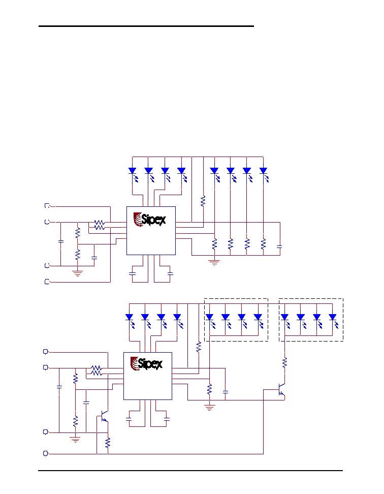
CIRCUIT DESCRIPTION
6
Date: 12/21/04
SP7683 Four Channel Charge Pump LED Driver © Copyright 2004 Sipex Corporation
The Low Dropout Regulator
The low dropout regulator provides matched currents into four LEDs. The current in the LED can
be programmed by an external resistor connected between the V
OUT
and I
SET
pins.
I
LED
= 200*(V
OUT
- 0.5)/R
SET
where the 200 is the Output Current Multiplying Ratio and 0.5 is I
SET
voltage value.
Board Layout and Grounding
To obtain the best performance from the SP7683, a printed circuit board with ground plane is
required. High quality, low series resistance ceramic 0.1µF bypass capacitors should be used at
the V
IN
and V
OUT
pins (pin 10 and 7). These capacitors and flying capacitors C1 and C2 must be
located as close to the part as possible. The traces connecting the pins to these capacitors should
be made as short and wide as possible.
CIRCUIT DESCRIPTION
R1
50k - 200k
GND
D5
D6
D7
R7
D8
R8
R6
R3
100k
LED_EN
U1
SP7683
R5
20
R4
270k
R9
100k
C1
1uF
C5
1uF
C4
1uF
C2
1uF
R2
1M
D1
D2
EN
Vin
D3
D4
C3
0.1uF
R1
50k - 200k
GND
D5
D6
D7
D8
R4
100k
LED_EN
U1
SP7683
R6
R5
270k
R7
100k
C1
1uF
C5
1uF
C4
1uF
C2
1uF
R3
1M
D1
D2
EN
Vin
D3
D4
C3
0.1uF
Q1
Q2
R8
R2
D9
D10
D11
D12
®
®
SP7683
1
2
7
4
6
5
3
9
8
12
13
10
11
14
15 16
®
®
SP7683
1
2
7
4
6
5
3
9
8
12
13
10
11
14
15 16
7
Date: 12/21/04
SP7683 Four Channel Charge Pump LED Driver © Copyright 2004 Sipex Corporation
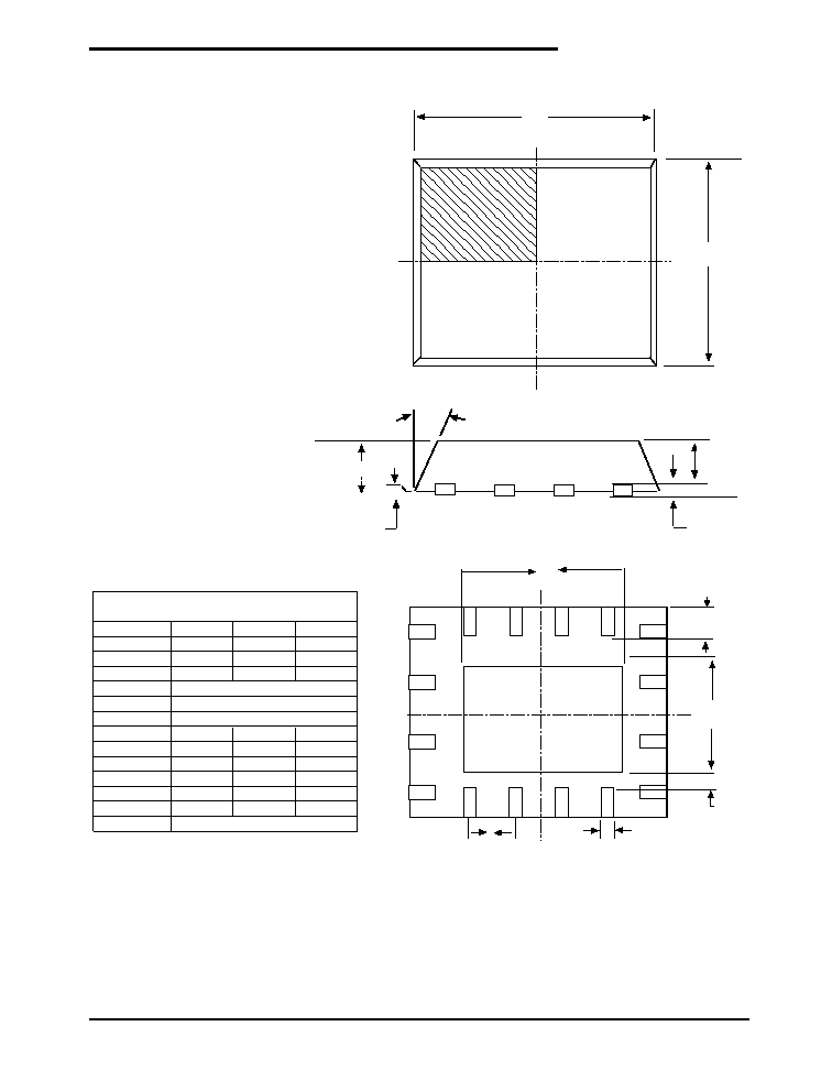
PACKAGE: 16 PIN QFN
16 PIN QFN
SEATING PLANE
A1
A
4 X
Ø
º
A3
A2
D2
NX L
E2
NX K
NX b
e
D
E
SYMBOL
MIN
NOM
MAX
A
0.8
0.9
1
A1
0
0.02
0.05
A2
0
0.65
1
A3
D
E
E2
7.4
7.8
8.2
D2
2.2
2.4
2.6
E2
2.2
2.4
2.6
L
0.45
0.55
0.65
K
0.2
-
-
b
0.25
0.3
0.35
e
Note: Dimensions in (mm)
0.65 BSC
16 Pin QFN JEDEC MO-220 VGGC-4
Variation
0.20 REF
4.00 BSC
4.00 BSC
8
Date: 12/21/04
SP7683 Four Channel Charge Pump LED Driver © Copyright 2004 Sipex Corporation
Corporation
ANALOG EXCELLENCE
Sipex Corporation reserves the right to make changes to any products described herein. Sipex does not assume any liability arising out of the
application or use of any product or circuit described herein; neither does it convey any license under its patent rights nor the rights of others.
Sipex Corporation
Headquarters and
Sales Office
233 South Hillview Drive
Milpitas, CA 95035
TEL: (408) 934-7500
FAX: (408) 935-7600
ORDERING INFORMATION
Part Number
Operating Temperature Range
Package Type
SP7683ER .................................................. -40°C to +85°C ............................................ 16 Pin 4 x 4mm QFN
SP7683ER/TR ............................................ -40°C to +85°C ............................................ 16 Pin 4 x 4mm QFN
Available in lead free packaging. To order add "-L" suffix to part number.
Example: SP7683ER/TR = standard; SP7683ER-L/TR = lead free
/TR = Tape and Reel
Pack quantity is 2500 for QFN.
CLICK HERE TO ORDER SAMPLES