 | –≠–ª–µ–∫—Ç—Ä–æ–Ω–Ω—ã–π –∫–æ–º–ø–æ–Ω–µ–Ω—Ç: SP7800AJN | –°–∫–∞—á–∞—Ç—å:  PDF PDF  ZIP ZIP |
SP7800ADS/02
SP7800A 12-Bit 3
µ
s Sampling A/D Converter
© Copyright 2000 Sipex Corporation
1
s
333k Samples Per Second
s
Standard
±
10V and
±
5V Input
s
No Missing Codes Over Temperature
s
AC Performance Over Temperature
71.5dB Signal≠to≠Noise Ratio at Nyquist
85dB Spurious≠free Dynamic Range at
49KHz
≠81dB Total Harmonic Distortion at
49KHz
s
Internal Sample/Hold, Reference,
Clock, and 3-State Outputs
s
Power Dissipation: 90mW
s
24≠Pin Narrow DIP and 24≠Lead SOIC
s
Enhanced Single (+5V) Supply Version of
ADS7800
DESCRIPTION...
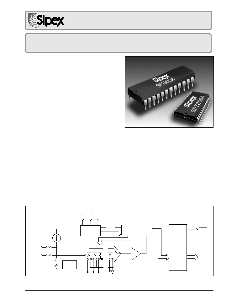
The SP7800A is a complete 12-bit sampling A/D converter using state≠of≠the≠art CMOS structures.
It contains a complete 12≠bit successive approximation A/D converter with internal sample/hold,
reference, clock, digital interface for microprocessor control, and three≠state output drivers. AC and
DC performance are completely specified. Two grades based on linearity and dynamic performance
are available to provide the optimum price/performance fit in a wide range of applications.
.....
.....
.....
.....
±10V
CS
R/C HBE
IBIP
IN
±5V
IN
Internal
Ref
Control
Logic
Clock
SAR
Comparator
Output
Latches
And
Three
State
Drivers
Three
State
Parallel
Output
Data
Bus
BUSY
CDAC
SP7800A
12-Bit 3
µ
s Sampling A/D Converter
Æ
SP7800ADS/02
SP7800A 12-Bit 3
µ
s Sampling A/D Converter
© Copyright 2000 Sipex Corporation
2
ABSOLUTE MAXIMUM RATINGS
These are stress ratings only and functional operation of the device
at these or any other above those indicated in the operation
sections of the specifications below is not implied. Exposure to
absolute maximum rating conditions for extended periods of time
may affect reliability.
V
S
to Digital Common ............................................................... +7V
Pin 23 (V
SO
) to Pin 24 (V
SA
) ....................................................
±
0.3V
Analog Common to Digital Common ......................................
±
0.3V
Control Inputs to Digital Common ....................... ≠0.3 to V
S
+ 0.3 V
Analog Input Voltage ..............................................................
±
20V
Maximum Junction Temperature ........................................... 160
∞
C
Internal Power Dissipation .................................................. 750mW
Lead Temperature (soldering, 10s) ..................................... +300
∞
C
Thermal Resistance. ÿ
JA
:
Plastic DIP ....................................................................... 50
∞
C/W
SOIC ............................................................................ 100
∞
CC/W
SPECIFICATIONS
T
A
= 25
∞
C, Sampling Frequency, f
8
, = 333kHz, V
S
= +5V, unless otherwise specified.
PARAMETER
MIN .
TYP.
MAX .
UNITS
CONDITIONS
RESOLUTION
12
BITS
ANALOG INPUT
Voltage Ranges
±
10V/
±
5V
V
Impedance
±
10V Range
4.7
6.7
8.7
k
T
MIN
T
A
T
MAX
±
5V Range
2.7
3.9
5.1
k
T
MIN
T
A
T
MAX
THROUGHPUT SPEED
Conversion Time
2.6
2.7
µ
s
Conversion alone
Complete Cycle
333
µ
s
Acquisition plus conversion
Throughput Rate
3.0
kHz
DC ACCURACY
T
MIN
T
A
T
MAX
Full Scale Error
Note 1
≠J
±
0.50
%
≠K
±
0.35
%
Integral Linearity Error
Note 2
≠J
±
1
LSB
≠K
±
1
/2
LSB
Differential Linearity Error
≠J
±
1
LSB
≠K
±
3
/4
LSB
No Missing Codes
Guaranteed
Bipolar Zero
Note 1
≠J
±
4
LSB
≠K
±
2
LSB
Power Supply Sensitivity
Note 3
≠J
±
.1
LSB
≠K
±
0.5
LSB
AC ACCURACY
T
MIN
T
A
T
MAX
Spurious-Free Dynamic Range
≠J
74
77
dB
Note 4; f
IN
= 47kHz
≠K
77
80
dB
Total Harmonic Distortion
f
IN
= 47kHz
≠J
≠77
≠74
dB
≠K
≠80
≠77
dB
Two-tone Intermod. Distortion
f
IN1
= 24.4kHz (≠6dB); f
IN2
=
28.5kHz (-6dB)
≠J
≠77
≠74
dB
≠K
≠80
≠77
dB
SP7800ADS/02
SP7800A 12-Bit 3
µ
s Sampling A/D Converter
© Copyright 2000 Sipex Corporation
3
SPECIFICATIONS (continued)
T
A
= 25
∞
C, Sampling Frequency, f
8
, = 333kHz, V
S
= +5V, unless otherwise specified.
PARAMETER
MIN .
TYP.
MAX .
UNITS
CONDITIONS
AC ACCURACY
T
MIN
T
A
T
MAX
Signal to (Noise + Distortion) Ratio
f
IN
= 47kHz
≠J
67
70
dB
≠K
69
71.0
dB
Signal to Noise Ratio (SNR)
f
IN
= 47kHz
≠J
68
71
dB
≠K
70
71.5
dB
SAMPLING DYNAMICS
Aperture Delay
13
ns
Aperture Jitter
150
ps, rms
Transient Response
Note 5
≠J
130
ns
≠K
150
ns
Overvoltage Recovery
150
ns
Note 6
DIGITAL INPUTS
T
MIN
T
A
T
MAX
Logic Levels
V
IL
≠0.3
+0.8
V
V
IH
+2.4
+5.3
V
I
IL
≠5
µ
A
I
IH
+5
µ
A
DIGITAL OUTPUTS
Data Format
Parallel; 12-bit or 8-bit/4-bit
Data Coding
Binary; Offset Binary
V
OL
DGND
+0.4
V
I
SINK
= 1.6mA
V
OH
+2.4
V
DD
V
I
SOURCE
= 1.6mA
I
LEAKAGE
(High-Z State)
±
0.1
±
5
µ
A
POWER SUPPLY REQUIREMENTS
Rated Voltage
+4.75
+5.0
+5.25
V
V
S
(V
SA
and V
SD
)
Current
18
21
mA
I
S
Power Consumption
90
mW
ENVIRONMENTAL AND MECHANICAL
Specification
≠J, ≠K
0
+70
∞
C
Storage
≠65
+150
∞
C
Package
≠_N
24≠pin Narrow DIP
≠_S
24≠pin SOIC
NOTES
1.
Adjustable to zero with external potentiometer.
2.
LSB means Least Significant Bit. For SP7800A, 1LSB = 2.44mV for
±
5V range, 1 LSB = 4.88mV for
±
10V range.
3.
Measured at mid-range, between 4.75 < V
S
< 5.25 volts.
4.
All specifications in dB are referred to a full-scale input, either
±
10V or
±
5V.
5.
For full-scale step input, 12-bit accuracy attained in specified time.
6.
Recovers to specified performance in specified time after 2 x F
S
input overvoltage.
SP7800ADS/02
SP7800A 12-Bit 3
µ
s Sampling A/D Converter
© Copyright 2000 Sipex Corporation
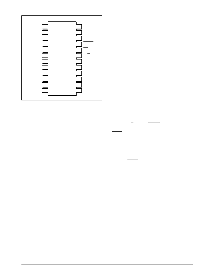
4
24 V
SA
23 V
SD
22 N.C.
21 BUSY
20 CS
19 R/C
18 HBE
17 D
0
16 D
1
15 D
2
14 D
3
13 DGND
IN
1
1
IN
2
2
N.C. 3
AGND 4
D
11
5
D
10
6
D
9
7
D
8
8
D
7
9
D
6
10
D
5
11
D
4
12
SP7800A
PINOUT
Pin 12 -- D
4
-- Data Bit 4 if HBE is LOW; LOW if
HBE is HIGH.
Pin 13 -- DGND -- Digital Ground. Connect to pin
4 at the device.
Pin 14 -- D
3
-- Data Bit 3 if HBE is LOW; Data Bit
11 if HBE is HIGH.
Pin 15 -- D
2
-- Data Bit 2 if HBE is LOW; Data Bit
10 if HBE is HIGH.
Pin 16 -- D
1
-- Data Bit 1 if HBE is LOW; Data Bit
9 if HBE is HIGH.
Pin 17 -- D
0
-- Data Bit 0 if HBE is LOW. Least
Significant Bit (LSB). Data Bit 8 if HBE is HIGH.
Pin 18 -- HBE -- High Byte Enable, When held
LOW, data output as 12-bits in parallel. When held
HIGH, four MSBs presented on pins 14≠17, pins 9 ≠
12 output LOWs. Must be LOW to initiate conver-
sion.
Pin 19 -- R/C -- Read/Convert. Falling edge initiates
conversion when CS is LOW, HBE is LOW, and
BUSY is HIGH.
Pin 20 -- CS -- Chip Select. Outputs in Hi-Z state
when HIGH. Must be LOW to initiate conversion or
read data.
Pin 21 -- BUSY . Output LOW during conversion.
Data valid on rising edge in Convert Mode.
Pin 22 -- N.C. -- This pin is not internally connected.
Pin 23 -- V
SD
-- Positive Digital Power Supply, +5V.
Connect to pin 24, and bypass to DGND.
Pin 24 -- V
SA
-- Positive Analog Power Supply.
+5V. Connect to pin 23, and bypass to AGND.
PIN ASSIGNMENT
Pin 1 -- IN
1
--
±
10V Analog Input. Connected to
AGND for
±
5V range.
Pin 2 -- IN
2
--
±
5V Analog Input. Connected to
AGND for
±
10V range.
Pin 3 -- N.C. -- This pin is not internally connected.
Pin 4 -- AGND -- Analog Ground. Connect to pin
13 at the device.
Pin 5 -- D
11
-- Data Bit 11. Most Significant Bit
(MSB).
Pin 6 -- D
10
-- Data Bit 10.
Pin 7 -- D
9
-- Data Bit 9.
Pin 8 -- D
8
-- Data Bit 8.
Pin 9 -- D
7
-- Data Bit 7 if HBE is LOW; LOW if
HBE is HIGH.
Pin 10 -- D
6
-- Data Bit 6 if HBE is LOW; LOW if
HBE is HIGH.
Pin 11 -- D
5
-- Data Bit 5 if HBE is LOW; LOW if
HBE is HIGH.
FEATURES...
The SP7800A is specified at a 333kHz sampling rate.
Conversion time is factory set for 2.70
µ
s max over
temperature, and the high-speed sampling input stage
insures a total acquisition and conversion time of 3
µ
s
max over temperature. Precision, laser≠trimmed scal-
SP7800ADS/02
SP7800A 12-Bit 3
µ
s Sampling A/D Converter
© Copyright 2000 Sipex Corporation
5
ing resistors provide industry≠standard input ranges
of
±
5V or
±
10V. The 24-pin SP7800A is available in
plastic DIP, and SOIC packages and it operates from
a single +5V supply. The SP7800A is available in
grades specified over the 0
∞
C to +70
∞
C commercial
temperature ranges.
edge of R/C will enable the output data pins, and
the data from the previous conversion becomes
valid. The falling edge then puts the SP7800A in
a hold mode, and initiates a new conversion.
The SP7800A will begin acquiring a new sample
just prior to BUSY output rising, and will track the
input signal until the next conversion is started.
For use with an 8-bit bus, the data can be read out
in two bytes under the control of HBE. With a
LOW input on HBE, at the end of a conversion, the
8 LSBs of data are loaded into the output drivers D
7
≠ D
4
and D
3
≠D
0
. Taking HBE HIGH then loads the
4 MSBs on output drivers D
3
≠D
0
, with D
7
≠D
4
being forced LOW.
Analog Input Ranges
The SP7800A offers two standard bipolar input
ranges:
±
10V and
±
5V. If a
±
10V range is re-
quired, the analog input signal should be con-
nected to pin 1. A signal requiring a
±
5V range
should be connected to pin 2. In either case, the
other pin of the two must be grounded or connected
to the adjustment circuits described in the section
on calibration.
Controlling The SP7800A
The SP7800A can be easily interfaced to most
microprocessor-based and other digital systems. The
microprocessor may take full control of each conver-
sion, or the SP7800A may operate in a stand-alone
mode, controlled only by the R/C input. Full control
consists of initiating the conversion and reading the
output data at user command, transmitting data either
all 12-bits in one parallel word, or in two 8-bit bytes.
The three control inputs (CS, R/C and HBE) are all
TTL/CMOS compatible. The functions of the control
lines are shown in Table 1.
For stand-alone operation, control of the SP7800A
is accomplished by a single control line connected
to R/C. In this mode, CS and HBE are connected
to GND. The output data are presented as 12-bit
words. The stand-alone mode is used in systems
containing dedicated input ports which do not
require full bus interface capability.
Conversion is initiated by a HIGH-to-LOW transition
OPERATION...
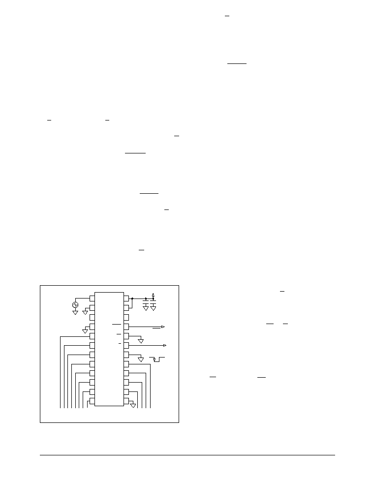
Basic Operation
Figure 1 shows the simple hookup circuit required
to operate the SP7800A in a
±
10V range in the
Convert Mode. A convert command arriving on
R/C, (a pulse taking R/C LOW for a minimum of
40ns) puts the SP7800A in the HOLD mode, and
a conversion is started. The falling edge of R/C
establishes the sampling instant of the A/D; it must
therefore have very low jitter. BUSY will be held
LOW during the conversion, and rises only after
the conversion is completed and the data has been
transferred to the output drivers. Thus, the rising
edge can be used to read the data from the conver-
sion. Also, during conversion, the BUSY signal
puts the output data lines in Hi-Z states and inhibits
the input lines. This means that pulses on R/C are
ignored, so that new conversions cannot be initi-
ated during a conversion, either as a result of
spurious signals or to short-cycle the SP7800A.
In the Read Mode, the input to R/C is kept nor-
mally LOW, and a HIGH pulse is used to read data
and initiate a conversion. In this mode, the rising
Figure 1. Basic
±
10V Operation
1
2
3
4
5
6
7
8
9
10
11
12
24
23
22
21
20
19
18
17
16
15
14
13
D0
(LSB)
Busy
Convert
Command
0.1µF
6.8µF +
+5V
+5V
+5V
N.C.
BUSY
CS
R/C
HBE
D0 (LSB)
D1
D2
D3
DGND
IN 1
IN 2
N.C.
AGND
D11 (MSB)
D10
D9
D8
D7
D6
D5
D4
D11
(MSB)
Data
Out
Input