 | –≠–ª–µ–∫—Ç—Ä–æ–Ω–Ω—ã–π –∫–æ–º–ø–æ–Ω–µ–Ω—Ç: SP782CT | –°–∫–∞—á–∞—Ç—å:  PDF PDF  ZIP ZIP |
1
SP782/SP784 DS/08
SP782/784 Programmable Charge Pump
© Copyright 2000 Sipex Corporation
SP782/784
Programmable Charge Pump
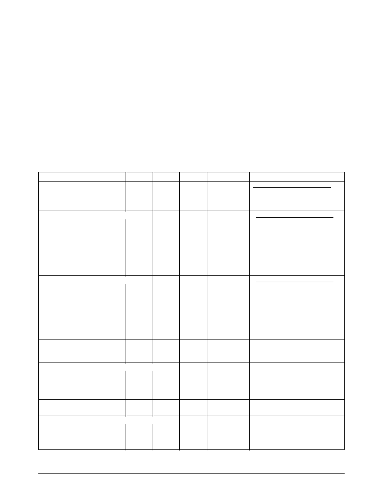
The SP782 and SP784 are monolithic programmable voltage converters that produce a
positive and negative voltage from a single supply. The SP782 and SP784 are programmable
such that the charge pump outputs either a
±
10V voltage or a
±
5V voltage by control of two
pins. Both products require four (4) charge pump capacitors to support the resulting output
voltages. The charge pump architecture (U.S. 5,760,637) is fabricated using a low power
BiCMOS process technology.
The SP782 and SP784 charge pumps can be powered from a single +5V supply. The low
power consumption makes these charge pumps ideal for battery operated equipment. Both
offer a shutdown feature that saves battery life. A system can essentially have four (4) different
supply voltages from a single battery. Typical applications are handheld instruments,
notebook and laptop computers, and data acquisition systems.
DESCRIPTION...
s
+5V Only Low Power Voltage Conversion
s
Programmable Between
±
5V or
±
10V
s
Low Power Shutdown Mode
Applications
s
RS-232/RS-423 transceiver power supplies
s
LCD BIAS Generator
s
OP-Amp Power Supplies
11
+5V
10
µ
F
+
GND
V
SS
13
V
CC
V
DD
2
SP782
C1+
C1≠
C2+
C2≠
1
µ
F
1
µ
F
1
µ
F
14
1
5
3
1
µ
F
16
C2+
12
D0
D1
9
8
4
6
LATCH
SD
15
11
+5V
10
µ
F
+
8
9
6
15
GND
16
V
SS
13
V
CC
V
DD
D0
D1
LATCH
SD
2
SP784
C1+
C1≠
C2+ (a)
C2≠
10
µ
F
10
µ
F
10
µ
F
14
1
5
3
10
µ
F
12
4
C2+ (b)
Æ
2
SP782/SP784 DS/08
SP782/784 Programmable Charge Pump
© Copyright 2000 Sipex Corporation
ABSOLUTE MAXIMUM RATINGS
These are stress ratings only and functional operation
of the device at these ratings or any other above those
indicated in the operation sections of the specifications
below is not implied. Exposure to absolute maximum
rating conditions for extended periods of time may
affect reliability.
V
CC
...........................................................................+7V
V
DD
.........................................................................+11V
V
SS
.........................................................................≠11V
Storage Temperature..........................-65∞C to +150∞C
Power Dissipation
16-pin Plastic DIP...........................1000mW
16-pin Plastic SOIC.........................1000mW
Package Derating:
16-pin Plastic DIP
¯
JA
....................................................62
∞
C/W
16-pin Plastic SOIC
¯
JA
....................................................62
∞
C/W
SP782 SPECIFICATIONS
Typical @ 25
∞
C and V
CC
= V
CC
±
5% unless otherwise noted.
MIN.
TYP.
MAX.
UNITS
CONDITIONS
SUPPLY CURRENT
CHARGE PUMP CAPACITORS: 1
µ
F
I
CC
3
8
mA
V
CC
= +5V, R
L
=
, V
O
= 2
x
V
CC
1
2
mA
V
CC
= +5V, R
L
=
, V
O
= V
CC
Shutdown I
CC
10
25
µ
A
V
CC
= +5V, SD = V
CC
POSITIVE CHARGE PUMP OUTPUT
CHARGE PUMP CAPACITORS: 1
µ
F
V
DD
(2
x
V
CC
Output)
+9.5
+9.8
+10.0
Volts
V
CC
= +5V, D
0
= 0V, D
1
= 0V
R
L
=
+8.0
+8.5
Volts
V
CC
= +5V, D
0
= 0V, D
1
= 0V
R
L
= 1k
V
DD
(V
CC
Output)
+4.2
+4.5
+5.0
Volts
V
CC
= +5V, D
0
= V
CC
, D
1
= V
CC
R
L
=
+4.2
+4.5
Volts
V
CC
= +5V, D
0
= V
CC
, D
1
= V
CC
R
L
= 1k
NEGATIVE CHARGE PUMP OUTPUT
CHARGE PUMP CAPACITORS: 1
µ
F
V
SS
(2
x
V
CC
Output)
≠9.5
≠9.8
≠10.0
Volts
V
CC
= +5V, D
0
= 0V, D
1
= 0V
R
L
=
≠8.0
≠8.5
Volts
V
CC
= +5V, D
0
= 0V, D
1
= 0V
R
L
= 1k
V
SS
(≠V
CC
Output)
≠4.2
≠4.5
≠5.0
Volts
V
CC
= +5V, D
0
= V
CC
, D
1
= V
CC
R
L
=
≠4.0
≠4.2
Volts
V
CC
= +5V, D
0
= V
CC
, D
1
= V
CC
R
L
= 1k
OSCILLATOR FREQUENCY
f
OSC
300
kHz
SD = 0V
VOLTAGE CONVERSION EFFICIENCY
V
DD
(2X V
CC
Output)
95
98
%
R
L
=
V
DD
(2X V
CC
Output)
80
85
%
R
L
= 1k
V
SS
(2X V
CC
Output)
85
90
%
R
L
=
V
SS
(2X V
CC
Output)
80
85
%
R
L
= 1k
POWER REQUIREMENTS
V
CC
+4.75
+5.25
Volts
ENVIRONMENTAL AND MECHANICAL
Operating Temperature Range
0
+70
∞
C
Storage Temperature Range
≠65
+150
∞
C
3
SP782/SP784 DS/08
SP782/784 Programmable Charge Pump
© Copyright 2000 Sipex Corporation
ABSOLUTE MAXIMUM RATINGS
These are stress ratings only and functional operation
of the device at these ratings or any other above those
indicated in the operation sections of the specifications
below is not implied. Exposure to absolute maximum
rating conditions for extended periods of time may
affect reliability.
V
CC
...........................................................................+7V
V
DD
.........................................................................+11V
V
SS
.........................................................................≠11V
Storage Temperature..........................-65∞C to +150∞C
Power Dissipation
16-pin Plastic DIP...........................1000mW
16-pin Plastic SOIC.........................1000mW
Package Derating:
16-pin Plastic DIP
¯
JA
....................................................62
∞
C/W
16-pin Plastic SOIC
¯
JA
....................................................62
∞
C/W
SP784 SPECIFICATIONS
Typical @ 25
∞
C and V
CC
= V
CC
±
5% unless otherwise noted.
MIN.
TYP.
MAX.
UNITS
CONDITIONS
SUPPLY CURRENT
CHARGE PUMP CAPACITORS: 10
µ
F
I
CC
5
10
mA
V
CC
= +5V, R
L
=
, V
O
= 2
x
V
CC
1
5
mA
V
CC
= +5V, R
L
=
, V
O
= V
CC
Shutdown I
CC
10
25
µ
A
V
CC
= +5V, SD = V
CC
POSITIVE CHARGE PUMP OUTPUT
CHARGE PUMP CAPACITORS: 10
µ
F
V
DD
(2
x
V
CC
Output)
+9.0
+9.8
+10.0
Volts
V
CC
= +5V, D
0
= 0V, D
1
= 0V
R
L
=
+8.0
+9.5
Volts
V
CC
= +5V, D
0
= 0V, D
1
= 0V
R
L
= 1k
V
DD
(V
CC
Output)
+4.5
+4.8
+5.0
Volts
V
CC
= +5V, D
0
= V
CC
, D
1
= V
CC
R
L
=
+4.2
+4.5
Volts
V
CC
= +5V, D
0
= V
CC
, D
1
= V
CC
R
L
= 1k
NEGATIVE CHARGE PUMP OUTPUT
CHARGE PUMP CAPACITORS: 10
µ
F
V
SS
(2
x
V
CC
Output)
≠9.0
≠9.8
≠10.0
Volts
V
CC
= +5V, D
0
= 0V, D
1
= 0V
R
L
=
≠8.0
≠9.5
Volts
V
CC
= +5V, D
0
= 0V, D
1
= 0V
R
L
= 1k
V
SS
(≠V
CC
Output)
≠4.2
≠4.5
≠5.0
Volts
V
CC
= +5V, D
0
= V
CC
, D
1
= V
CC
R
L
=
≠4.0
≠4.2
Volts
V
CC
= +5V, D
0
= V
CC
, D
1
= V
CC
R
L
= 1k
OSCILLATOR FREQUENCY
f
OSC
300
kHz
SD = 0V
VOLTAGE CONVERSION EFFICIENCY
V
DD
(2X V
CC
Output)
90
98
%
R
L
=
V
DD
(2X V
CC
Output)
80
95
%
R
L
= 1k
V
SS
(2X V
CC
Output)
90
98
%
R
L
=
V
SS
(2X V
CC
Output)
80
95
%
R
L
= 1k
POWER REQUIREMENTS
V
CC
+4.75
+5.25
Volts
ENVIRONMENTAL AND MECHANICAL
Operating Temperature Range
0
+70
∞
C
Storage Temperature Range
≠65
+150
∞
C
4
SP782/SP784 DS/08
SP782/784 Programmable Charge Pump
© Copyright 2000 Sipex Corporation
AC CHARACTERISTICS*
(Typical @ 25
∞
C and nominal supply voltages unless otherwise noted)
PARAMETER
MIN.
TYP.
MAX.
UNITS
CONDITIONS
SP782 POWER-UP DELAY TIME
±
10V OUTPUT
t
DVDD
; V
DD
Power On Delay
1000
µ
s
R
L
= 1k
t
DVSS
; V
SS
Power-On Delay
1000
µ
s
R
L
= 1k
±
5V OUTPUT
t
DVDD
; V
DD
Power On Delay
10
µ
s
R
L
= 1k
t
DVSS
; V
SS
Power-On Delay
150
µ
s
R
L
= 1k
SP782 OUTPUT DELAY TIME
t
SD1
; Switching Delay
1000
µ
s
R
L
= 1k
from
±
10V to
±
5V
t
SD2
; Switching Delay
500
µ
s
R
L
= 1k
from
±
5V to
±
10V
SP784 POWER-UP DELAY TIME
±
10V OUTPUT
t
DVDD
; V
DD
Power On Delay
5
ms
R
L
= 1k
t
DVSS
; V
SS
Power-On Delay
5
ms
R
L
= 1k
±
5V OUTPUT
t
DVDD
; V
DD
Power On Delay
10
µ
s
R
L
= 1k
t
DVSS
; V
SS
Power-On Delay
1000
µ
s
R
L
= 1k
SP784 OUTPUT DELAY TIME
t
SD1
; Switching Delay
10
ms
R
L
= 1k
from
±
10V to
±
5V
t
SD2
; Switching Delay
2
ms
R
L
= 1k
from
±
5V to
±
10V
* - Using the charge pump capacitor values specified in the previous pages for each device.
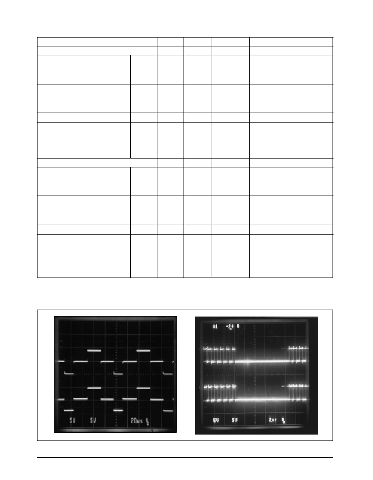
Figure 1. Charge Pump Waveforms
≠10V
+10V
C
2
+
C
2
≠
(a)
(b)
C
2
+
+5V
GND
GND
C
2
≠
≠5V
GND
GND
5
SP782/SP784 DS/08
SP782/784 Programmable Charge Pump
© Copyright 2000 Sipex Corporation
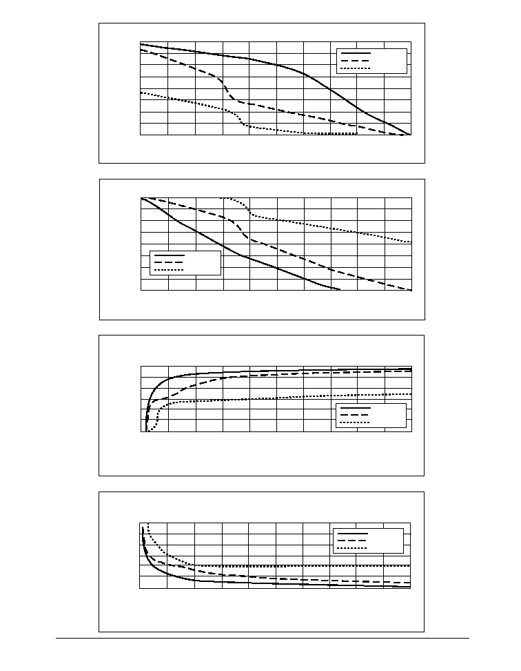
SP782 VDD vs IDD D0 = D1 = 0V VCC = 5.00V T = +25
O
C
40.00
35.00
30.00
25.00
20.00
15.00
10.00
5.00
0.00
IDD(milliamps)
5.00
5.50
6.00
6.50
7.00
7.50
8.00
8.50
9.00
9.50 10.00
VDD(volts)
10uF Curve
1uF Curve
0.1uF Curve
SP782 VSS vs ISS D0 = D1 = 0V VCC = 5.00V T = +25
O
C
0.00
-5.00
-10.00
-15.00
-20.00
-25.00
-30.00
-35.00
-40.00
ISS(milliamps)
VSS(volts)
10uF Curve
1uF Curve
0.1uF Curve
-5.00
-5.50
-6.00
-6.50
-7.00
-7.50
-8.00
-8.50
-9.00
-9.50
-10.00
SP782 LOAD vs VDD D0 = D1 = 0V VCC = 5.00V T = +25
O
C
10.00
9.00
8.00
7.00
6.00
5.00
4.00
VDD (volts)
VDD - 10uF
VDD - 1uF
VDD - 0.1uF
-4.00
-5.00
-6.00
-7.00
-8.00
-9.00
-10.00
0
500
1000
1500
2000
2500
3000
3500 4000
4500
5000
LOAD(ohms)
VSS - 10uF
VSS - 1uF
VSS - 0.1uF
0
500
1000
1500
2000
2500
3000
3500 4000
4500
5000
LOAD (ohms)
SP782 LOAD vs VSS D0 = D1 = 0V VCC = 5.00V T = +25
O
C
VSS (volts)
6
SP782/SP784 DS/08
SP782/784 Programmable Charge Pump
© Copyright 2000 Sipex Corporation
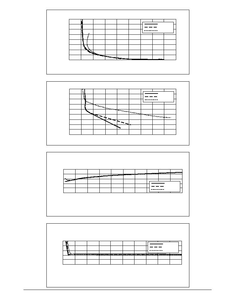
SP782 VDD vs IDD D0 = D1 = 5V VCC = 5.00V T = +25
O
C
40.00
35.00
30.00
25.00
20.00
15.00
10.00
5.00
0.00
IDD(milliamps)
4.20
4.25
4.30
4.35
4.40
4.45
4.50
4.55
4.60
4.65
VDD(volts)
10uF Curve
1uF Curve
0.1uF Curve
SP782 VSS vs ISS D0 = D1 = 5V VCC = 5.00V T = +25
O
C
0.00
-5.00
-10.00
-15.00
-20.00
-25.00
-30.00
-35.00
-40.00
-45.00
ISS(milliamps)
VSS(volts)
10uF Curve
1uF Curve
0.1uF Curve
-3.50
-3.60
-3.70
-3.80
-3.90
-4.00
-4.10
-4.20
-4.30
-4.40
SP782 LOAD vs VDD D0 = D1 = 5V VCC = 5.00V T = +25
O
C
4.50
4.40
4.30
4.20
4.10
4.00
VDD (volts)
VDD - 10uF
VDD - 1uF
VDD - 0.1uF
-4.00
-4.10
-4.20
-4.30
-4.40
-4.50
0
500
1000
1500
2000
2500
3000
3500 4000
4500
5000
LOAD(ohms)
VSS - 10uF
VSS - 1uF
VSS - 0.1uF
0
500
1000
1500
2000
2500
3000
3500 4000
4500
5000
LOAD(ohms)
VSS (volts)
SP782 LOAD vs VSS D0 = D1 = 5V VCC = 5.00V T = +25
O
C
7
SP782/SP784 DS/08
SP782/784 Programmable Charge Pump
© Copyright 2000 Sipex Corporation
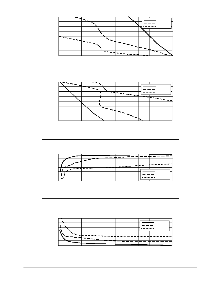
SP784 VDD vs IDD D0 = D1 = 0V VCC = 5.00V T = +25
O
C
40.00
35.00
30.00
25.00
20.00
15.00
10.00
5.00
0.00
IDD(milliamps)
5.00
5.50
6.00
6.50
7.00
7.50
8.00
8.50
9.00
9.50 10.00
VDD(volts)
10uF Curve
1uF Curve
0.1uF Curve
SP784 VSS vs ISS D0 = D1 = 0V VCC = 5.00V T = +25
O
C
0.00
-5.00
-10.00
-15.00
-20.00
-25.00
-30.00
-35.00
-40.00
ISS(milliamps)
VSS(volts)
10uF Curve
1uF Curve
0.1uF Curve
-5.00
-5.50
-6.00
-6.50
-7.00
-7.50
-8.00
-8.50
-9.00
-9.50
-10.00
SP784 LOAD vs VDD D0 = D1 = 0V VCC = 5.00V T = +25
O
C
10.00
9.00
8.00
7.00
6.00
5.00
4.00
VDD (volts)
VDD - 10uF
VDD - 1uF
VDD - 0.1uF
-4.00
-5.00
-6.00
-7.00
-8.00
-9.00
-10.00
0
500
1000
1500
2000
2500
3000
3500 4000
4500
5000
VSS - 10uF
VSS - 1uF
VSS - 0.1uF
0
500
1000
1500
2000
2500
3000
3500 4000
4500
5000
LOAD(ohms)
VSS (volts)
LOAD(ohms)
SP784 LOAD vs VSS D0 = D1 = 0V VCC = 5.00V T = +25
O
C
8
SP782/SP784 DS/08
SP782/784 Programmable Charge Pump
© Copyright 2000 Sipex Corporation
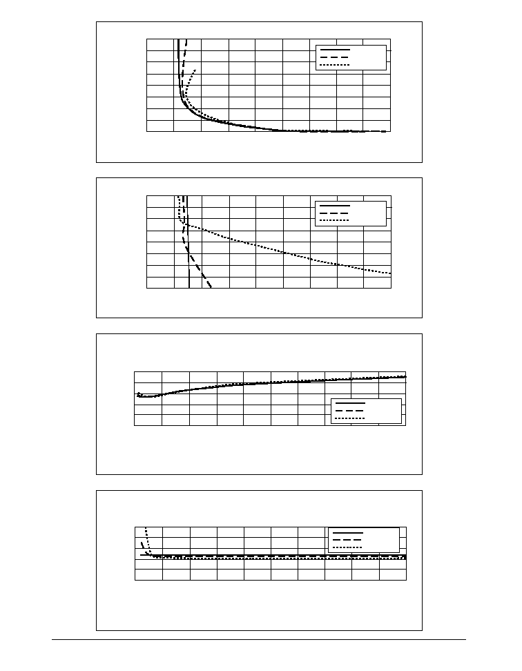
SP784 VDD vs IDD D0 = D1 = 5V VCC = 5.00V T = +25
O
C
40.00
35.00
30.00
25.00
20.00
15.00
10.00
5.00
0.00
IDD(milliamps)
4.20
4.25
4.30
4.35
4.40
4.45
4.50
4.55
4.60
4.65
VDD(volts)
10uF Curve
1uF Curve
0.1uF Curve
SP784 VSS vs ISS D0 = D1 = 5V VCC = 5.00V T = +25
O
C
0.00
-5.00
-10.00
-15.00
-20.00
-25.00
-30.00
-35.00
-40.00
ISS(milliamps)
VSS(volts)
10uF Curve
1uF Curve
0.1uF Curve
-3.50
-3.60
-3.70
-3.80
-3.90
-4.00
-4.10
-4.20
-4.30
-4.40
SP784 LOAD vs VDD D0 = D1 = 5V VCC = 5.00V T = +25
O
C
4.50
4.40
4.30
4.20
4.10
4.00
VDD (volts)
VDD - 10uF
VDD - 1uF
VDD - 0.1uF
-4.00
-4.10
-4.20
-4.30
-4.40
-4.50
0
500
1000
1500
2000
2500
3000
3500 4000
4500
5000
LOAD(ohms)
VSS - 10uF
VSS - 1uF
VSS - 0.1uF
0
500
1000
1500
2000
2500
3000
3500 4000
4500
5000
LOAD(ohms)
VSS (volts)
SP784 LOAD vs VSS D0 = D1 = 5V VCC = 5.00V T = +25
O
C
9
SP782/SP784 DS/08
SP782/784 Programmable Charge Pump
© Copyright 2000 Sipex Corporation
V
SS
receives a continuous charge from either C
1
or C
2
. With the C1 capacitor charged to 5V, the
cycle begins again.
Phase 3
-- V
DD
charge storage -- The third phase of the
clock is identical to the first phase -- the charge
transferred in C
1
produces ≠5V in the negative
terminal of C
1
, which is applied to the negative
side of capacitor C
2
. Since C
2
+
is at +5V, the
voltage potential across C
2
is l0V. For the 5V
output, C
2
+
is connected to ground so that the
potential on C
2
is only +5V.
Phase 4
-- V
DD
transfer -- The fourth phase of the
clock connects the negative terminal of C
2
to
ground and transfers the generated l0V or the
generated 5V across C
2
to C
4
, the V
DD
storage
capacitor. Again, simultaneously with this, the
positive side of capacitor C
1
is switched to +5V
and the negative side is connected to ground,
and the cycle begins again.
Since both V
DD
and V
SS
are separately gener-
ated from V
CC
in a no≠load condition, V
DD
and
V
SS
will be symmetrical. Older charge pump
approaches that generate V
≠
from V
+
will show
a decrease in the magnitude of V
≠
compared to
V
+
due to the inherent inefficiencies in the
design.
V
CC
= +5V
≠5V
≠5V
+5V
V
DD
Storage Capacitor
C
1
C
2
C
4
+
+
+
≠
≠
≠
V
SS
Storage Capacitor
C
3
+
≠
Figure 3. Charge Pump Phase 1 for
±
5V.
V
CC
= +5V
+5V
V
DD
Storage Capacitor
C
1
C
2
C
4
+
+
+
≠
≠
≠
V
SS
Storage Capacitor
C
3
+
≠
≠5V
Figure 2. Charge Pump Phase 1 for
±
10V.
THEORY OF OPERATION
The SP782/784's charge pump design is based
on Sipex's original patented charge pump de-
sign (5,306,954) which uses a four≠phase volt-
age shifting technique to attain symmetrical
10V power supplies. In addition, the SP782/
784 charge pump incorporates a "program-
mable" feature that produces an output of
±
10V
or
±
5V for V
SS
and V
DD
by two control pins, D0
and D1. The charge pump requires external
capacitors to store the charge. Figure 1 shows
the waveform found on the positive and nega-
tive side of capcitor C2. There is a free≠running
oscillator that controls the four phases of the
voltage shifting. A description of each phase
follows.
Phase 1 (
±
10V)
-- V
SS
charge storage -- During this phase of
the clock cycle, the positive side of capacitors
C
1
and C
2
are initially charged to +5V. C
l
+
is
then switched to ground and the charge on C
1
≠
is transferred to C
2
≠
. Since C
2
+
is connected to
+5V, the voltage potential across capacitor C
2
is now 10V.
Phase 1 (
±
5V)
-- V
SS
& V
DD
charge storage and transfer --
With the C
1
and C
2
capacitors initially charged
to +5V, C
l
+
is then switched to ground and the
charge on C
1
≠
is transferred to the V
SS
storage
capacitor. Simultaneously the C
2
≠
is switched
to ground and 5V charge on C
2
+
is transferred
to the V
DD
storage capacitor.
Phase 2 (
±
10V)
-- V
SS
transfer -- Phase two of the clock
connects the negative terminal of C
2
to the V
SS
storage capacitor and the positive terminal of
C
2
to ground, and transfers the generated ≠l0V
or the generated ≠5V to C
3
. Simultaneously,
the positive side of capacitor C
1
is switched to
+5V and the negative side is connected to
ground.
Phase 2 (
±
5V)
-- V
SS
& V
DD
charge storage -- C
1
+
is
reconnected to V
CC
to recharge the C
1
capacitor. C
2
+
is switched to ground and C
2
≠
is
connected to C
3
.
The 5V charge from Phase 1 is
now transferred to the V
SS
storage capacitor.
10
SP782/SP784 DS/08
SP782/784 Programmable Charge Pump
© Copyright 2000 Sipex Corporation
Figure 4. Charge Pump Phase 2 for
±
10V.
The oscillator frequency or clock rate for
the charge pump is designed for low power
operation. The oscillator changes from a high
frequency mode (400kHz) to a low frequency
mode (20kHz) when the SD pin goes to a logic
"1". The lower frequency allows the
SP782/
SP784
to conserve power when the outputs are
not being used.
EFFICIENCY INFORMATION
A charge pump theoretically produces a doubled
voltage at 100% efficiency. However in the real
world, there is a small voltage drop on the output
which reduces the output efficiency. The SP782
and SP784 can usually run 99.9% efficient with-
out driving a load. While driving a 1k
load, the
SP782 and SP784 remain at least 90% efficient.
Total Output Voltage Efficiency =
[(V
OUT
+) / (2*V
CC
)] + [(V
OUT
≠) / (≠2*V
CC
)] ;
V
OUT
+ = 2*V
CC
+ V
DROP
+
V
OUT
≠ = ≠2*V
CC
+ V
DROP
≠
V
DROP
≠ = (I≠)*(R
OUT
≠)
V
DROP
+ = (I+)*(R
OUT
+)
Power Loss = I
OUT
*(V
DROP
)
The efficiency changes as the external charge
pump capacitors are varied. Larger capacitor
values will strengthen the output and reduce
output ripple usually found in all charge pumps.
Although smaller capacitors will cost less and
Figure 6. Charge Pump Phase 3.
V
CC
= +5V
≠10V
V
DD
Storage Capacitor
C
1
C
2
C
4
+
+
+
≠
≠
≠
V
SS
Storage Capacitor
C
3
+
≠
V
CC
= +5V
≠5V
≠5V
+5V
V
DD
Storage Capacitor
C
1
C
2
C
4
+
+
+
≠
≠
≠
V
SS
Storage Capacitor
C
3
+
≠
Figure 7. Charge Pump Phase 4.
Figure 5. Charge Pump Phase 2 for
±
5V.
V
CC
= +5V
V
DD
Storage Capacitor
C
1
C
2
C
4
+
+
+
≠
≠
≠
V
SS
Storage Capacitor
C
3
+
≠
≠5V
V
CC
= +5V
+10V
V
DD
Storage Capacitor
C
1
C
2
C
4
+
+
+
≠
≠
≠
V
SS
Storage Capacitor
C
3
+
≠
save board space, lower values will reduce the
output drive capability.
The output voltage ripple is also affected by the
capacitors, specifically C3 and C4. Larger val-
ues will reduce the output ripple for a given load
of current. The current drawn from either output
is supplied by just the storage capacitor, C3 or
C4, during one half cycle of the internal oscilla-
tor. Note that the output current from the postive
charge pump is the load current plus the current
taken by the negative charge pump. Thus the
formula representation for the output ripple
voltage is:
V
RIPPLE
+ = {1 / (f
OSC
) * 1 / C3} * 0.5 * I
OUT
+
V
RIPPLE
≠ = {1 / (f
OSC
) * 1 / C3} * 0.5 * I
OUT
≠
To minimize the output ripple, the C3 and C4
storage capacitors can be increased to over 10
µ
F
whereas the pump capacitors can range from
1
µ
F to 5
µ
F.
Multiple SP782/784 charge pumps can be
connected in parallel. However, the output
resistance on both pump outputs will be
reduced. The effective output resistance is the
output resistance of one pump divided by the
number of charge pumps connected. It is
important to keep the C1 and C2 capacitors
separate for each charge pump. The storage
capacitors, C3 and C4, can be shared.

11
SP782/SP784 DS/08
SP782/784 Programmable Charge Pump
© Copyright 2000 Sipex Corporation
SHUTDOWN MODE
The internal oscillator of the SP782 and SP784
can be shutdown through the SD pin. In this
state, the V
DD
and V
SS
outputs are inactive and
the power supply current reduces to 10
µ
A.
LATCH ENABLE PIN
The SP782 and SP784 includes a control pin
(LAT) that latches the D0 and D1 control lines.
Connecting this pin to a logic HIGH state will
allow transparent operation of the D0 and D1
control lines. This input can be left floating
since there is an internal pull-up resistor which
will allow the latch to be transparent.
APPLICATIONS INFORMATION
The SP782 and SP784 can be used in various
applications where
±
10V is needed from a +5V
source. Analog switches, op-amp power sup-
plies, and LCD biasing are some applications
where the charge pumps can be used.
The charge pump can also be used for supplying
voltage rails for RS-232 drivers needing
±
12V.
The
±
10V output from the charge pump is more
than adequate to provide the proper V
OH
and
V
OL
levels at the driver output.
Figure 8 shows how the SP784 can be used
in conjunction with the SP524 multiprotocol
transceiver IC. The programmability is ideal for
RS-232 and RS-423 levels. The RS-232 driver
output voltage swing ranges from
±
5V to
±
15V.
In order to meet this requirement, the charge
pump must generate
±
10V to the transceiver IC.
The RS-423 driver output voltage range is
±
4.0V to
±
6.0V. When the SP524 transceiver is
programmed to RS-423 mode (V.10), the charge
pump now provides
±
5V, through D0 and D1,
thus allowing the driver outputs to comply with
V
OC
6.0V as well as the V
T
requirement of
±
4.0V minimum with a 450
load to ground.
In older configurations, separate DC sources
needed to be configured or regulated down from
±
10V to
±
5V in a given application. A typical
charge pump providing V
DD
and V
SS
would
require external clamping such as 5V Zener
diodes. RS-423 (V.10) is usually found in
RS-449, EIA-530, EIA-530A, and V.36 modes.
When the control lines D0 and D1 are both at a
logic HIGH, V
DD
= +5V and V
SS
= -5V. All
other inputs to the control lines result in V
DD
=
+10V and V
SS
= -10V. Control of the SP784 in
an application with Sipex's SP524 can be found
in Figure 8.
12
SP782/SP784 DS/08
SP782/784 Programmable Charge Pump
© Copyright 2000 Sipex Corporation
Figure 8. SP784 Application w/ SP524 Multi-Protocol Transceiver IC.
T1IN
24
T1
T1OUTA
22
17
T2IN
25
T2
18
R1INA
44
R1OUT
43
R2OUT
T1OUTB
T2OUTA
T2OUTB
R1INB
R2INA
R2INB
LOOPBA
CK P
A
THS
V
DD
28
V
SS
+5V
V
CC
10
µ
F
14
+
ENT1
ENT2
ENR1
ENR2
SP524
DP0
DP1
LATCH_EN
LOOPBCK
DECODER LOGIC
40
36
35
39
20
3
4
5
6
31
32
30
23
T3IN
26
T3
T3OUTA
16
11
T4IN
27
T4
13
R3INA
42
R3OUT
41
R4OUT
T3OUTB
T4OUTA
T4OUTB
R3INB
R4INA
R4INB
LOOPBA
CK P
A
THS
ENT3
ENT4
ENR3
ENR4
38
34
33
37
15
7
8
9
10
GND
12
1
21
2
19
29
V
CC
V
CC
GND
GND
R2
R1
R3
R4
11
+5V
10
µ
F
+
8
9
6
15
GND
16
V
SS
13
V
CC
V
DD
D0
D1
EN
SD
2
SP784
C1+
C1≠
C2+ (a)
C2≠
10
µ
F
10
µ
F
10
µ
F
14
1
5
3
10
µ
F
12
4
C2+ (b)
D0
D1
V
DD
V
SS
0
0
+10V
-10V
0
1
+10V
-10V
1
0
+10V
-10V
1
1
+5V
-5V
13
SP782/SP784 DS/08
SP782/784 Programmable Charge Pump
© Copyright 2000 Sipex Corporation
Figure 9. SP782 and SP784 Block Diagrams
11
+5V
10
µ
F
+
GND
V
SS
13
V
CC
V
DD
2
SP782
C1+
C1≠
C2+
C2≠
1
µ
F
1
µ
F
1
µ
F
14
1
5
3
1
µ
F
16
C2+
12
D0
D1
9
8
4
6
LATCH
SD
15
11
+5V
10
µ
F
+
8
9
6
15
GND
16
V
SS
13
V
CC
V
DD
D0
D1
LATCH
SD
2
SP784
C1+
C1≠
C2+ (a)
C2≠
10
µ
F
10
µ
F
10
µ
F
14
1
5
3
10
µ
F
12
4
C2+ (b)
14
SP782/SP784 DS/08
SP782/784 Programmable Charge Pump
© Copyright 2000 Sipex Corporation
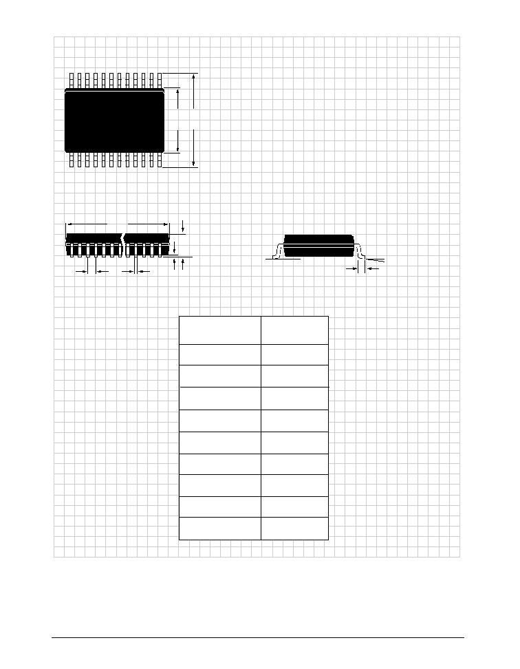
D
E
H
PACKAGE:
PLASTIC
SMALL OUTLINE (SOIC)
(WIDE)
DIMENSIONS (Inches)
Minimum/Maximum
(mm)
A
A1
ÿ
L
B
e
A
A1
B
D
E
e
H
L
ÿ
16≠PIN
0.093/0.104
(2.352/2.649)
0.004/0.012
(0.102/0.300)
0.013/0.020
(0.330/0.508)
0.398/0.406
(10.11/10.31)
0.291/0.299
(7.402/7.600)
0.050 BSC
(1.270 BSC)
0.394/0.419
(10.00/10.64)
0.016/0.050
(0.406/1.270)
0
∞
/8
∞
(0
∞
/8
∞
)
15
SP782/SP784 DS/08
SP782/784 Programmable Charge Pump
© Copyright 2000 Sipex Corporation
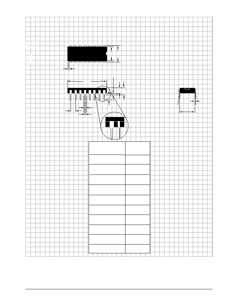
D
ALTERNATE
END PINS
(BOTH ENDS)
D1 = 0.005" min.
(0.127 min.)
E
PACKAGE:
16-PIN PLASTIC
DUAL≠IN≠LINE
(NARROW)
A
E1
C
ÿ
L
A2
A1 = 0.015" min.
(0.381min.)
B
B1
e = 0.100 BSC
(2.540 BSC)
e
A
= 0.300 BSC
(7.620 BSC)
DIMENSIONS (Inches)
Minimum/Maximum
(mm)
A
A2
B
B1
C
D
E
E1
L
ÿ
≠/0.210
(≠/5.334)
0.115/0.195
(2.921/4.953)
0.014/0.022
(0.356/0.559)
0.045/0.070
(1.143/1.778)
0.008/0.014
(0.203/0.356)
0.780/0.800
(19.812/20.320)
0.300/0.325
(7.620/8.255)
0.240/0.280
(6.096/7.112)
0.115/0.150
(2.921/3.810)
0
∞
/ 15
∞
(0
∞
/15
∞
)
16≠PIN
16
SP782/SP784 DS/08
SP782/784 Programmable Charge Pump
© Copyright 2000 Sipex Corporation
ORDERING INFORMATION
Model
Temperature Range
Package Types
SP782CP .......................................................................... 0
∞
C to +70
∞
C ..................................................................................... 16-pin Plastic DIP
SP784CP .......................................................................... 0
∞
C to +70
∞
C ..................................................................................... 16-pin Plastic DIP
SP782CT ........................................................................... 0
∞
C to +70
∞
C .............................................................................................. 16-pin SOIC
SP784CT ........................................................................... 0
∞
C to +70
∞
C .............................................................................................. 16-pin SOIC
Sipex Corporation reserves the right to make changes to any products described herein. Sipex does not assume any liability arising out of the
application or use of any product or circuit described hereing; neither does it convey any license under its patent rights nor the rights of others.
Corporation
SIGNAL PROCESSING EXCELLENCE
Please consult the factory for pricing and availability on a Tape-On-Reel option.
Sipex Corporation
Headquarters and
Sales Office
22 Linnell Circle
Billerica, MA 01821
TEL: (978) 667-8700
FAX: (978) 670-9001
e-mail: sales@sipex.com
Sales Office
233 South Hillview Drive
Milpitas, CA 95035
TEL: (408) 934-7500
FAX: (408) 935-7600