Date: 8/0/06 Rev G SP78MXX 500mA 3-Terminal Positive Voltage Regulator
© 2006 Sipex Corporation
general Description
The S
P78MXX series are monolithic integrated circuits designed as fixed-voltage regulators for a wide variety of
applications including local, on-card regulation.
This series of regulators are complete with internal current limiting, thermal shutdown protection, and safe-area
compensation which make them virtually immune from output overload. If adequate heat sinking are provided, these
regulators can deliver output currents up to 0.5A.
The S
P78MXX series are available in two standard plastic packages: TO-220 and TO-252.
Features
∑
Output Current up to 0.5A
∑
Fixed Output Voltages of 5V and 12V
∑
Output Voltage Tolerances of ± 5% over the Full
Temperature Range
∑
Internal Short Circuit Current-Limiting
∑
Internal Thermal Overload Protection
∑
Available in Lead Free, RoHS Compliant Packaging
Applications
∑
Consumer Electronics
∑
Microprocessor Power Supply
∑
Mother Board I/O Power Supply
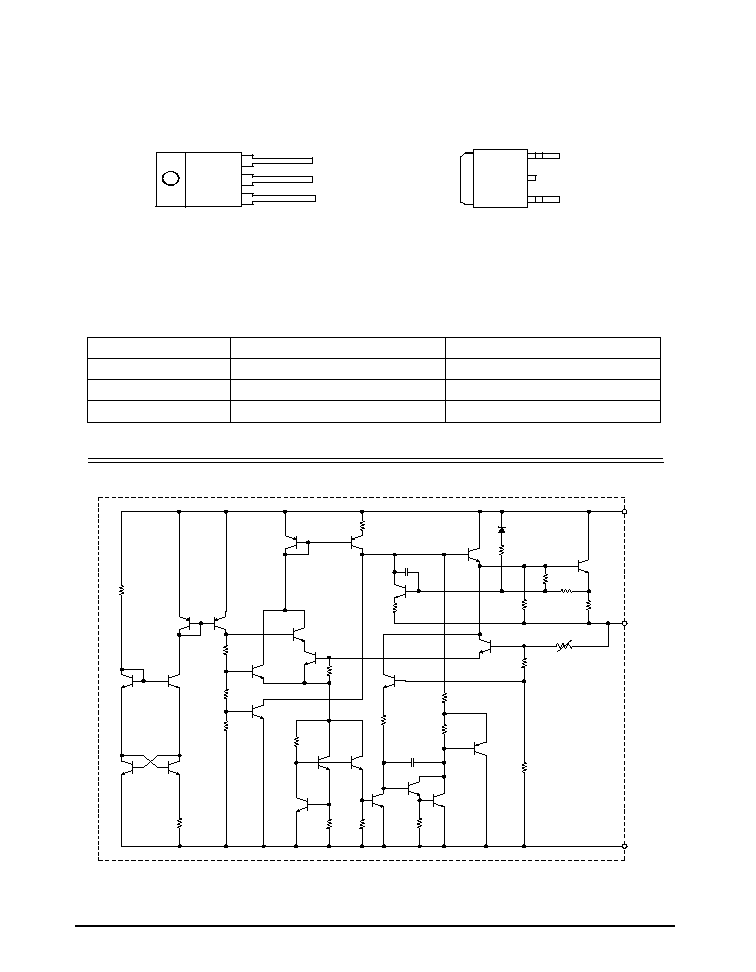
TO-220 Package
INPUT
OUTPUT
GND
1
2
3
TO-220
TO-252
Figure 1. Package Types of SP78MXX
SP78MXX
Solved by
TM
500mA 3-Terminal Positive Voltage Regulator
2
Date: 8/0/06 Rev G SP78MXX 500mA 3-Terminal Positive Voltage Regulator
© 2006 Sipex Corporation
Figure 2. Pin Configuration of SP78MXX (Top View)
V Package
(TO-220)
INPUT
OUTPUT
GND
1
2
3
1
2
3
INPUT
OUTPUT
GND
V
2 Package
(TO-252)
Pin configuration
Pin Description
Pin Number
Pin Name
Function
1
INPUT
Voltage Input
2
GND
Ground
3
OUTPUT
Voltage Output
Functional Block Diagram
Figure 3. Functional Block Diagram of SP78MXX
R9
R7
R4
R3
R5
C1
R11
R19
R18
R14
R15
R16
R17
R20
R23
R21
R2
2
OUTPUT
INPUT
R12
R2
R1
Q23
Q6
Q3
Q9
Q14
Q18
Q21
Q22
Q24
Q16
Q2
Q1
Q4
Q11
Q7
Q10
Q8
Q5
R8
R10
R6
R13
C2
Q12
Q15
Q13
Q17
Q19
Q20
GND
3
Date: 8/0/06 Rev G SP78MXX 500mA 3-Terminal Positive Voltage Regulator
© 2006 Sipex Corporation
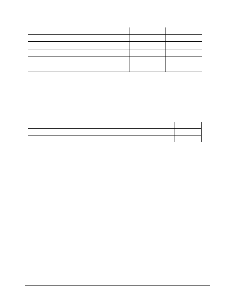
Parameter
Symbol
Value
Unit
Input Voltage
V
IN
20
V
Lead Temperature (Soldering, 10 sec.)
300
o
C
Power Dissipation
P
D
Internally Limited
Storage Temperature Range
T
STG
-65 to 150
o
C
ESD (Machine Model)
ESD
450
V
Note 1: Stresses greater than those listed under "Absolute Maximum Ratings" may cause permanent damage to
the device. These are stress ratings only, and functional operation of the device at these or any other conditions
beyond those indicated under "Recommended Operating Conditions" is not implied. Exposure to "Absolute Max-
imum Ratings" for extended periods may affect device reliability.
Recommended Operating conditions
Parameter
Symbol
Min
Max
Unit
Supply Voltage
V
CC
7.5
18
V
Operating Junction Temperature Range
T
J
-40
125
Absolute Maximum Ratings (note 1)

Date: 8/0/06 Rev G SP78MXX 500mA 3-Terminal Positive Voltage Regulator
© 2006 Sipex Corporation
Parameter
Symbol
Conditions
Min
Typ
Max
Unit
Output Voltage
V
OUT
T
J
=25
o
C
4.8
5
5.2
V
V
IN
=7V to 15V, I
OUT
=5mA to 350mA
4.75
5
5.25
V
Line Regulation
V
RLINE
T
J
=25
o
C, V
IN
=7V to 15V, I
OUT
=200mA
3
50
mV
Load Regulation
V
RLOAD
T
J
=25
o
C, I
OUT
=5mA to 500mA
20
100
mV
Quiescent Current
I
Q
T
J
=25
o
C
3.2
6
mA
Quiescent Current Change
I
Q
V
IN
=8V to 15V, I
OUT
=200mA
0.8
mA
I
OUT
=5mA to 350mA
0.5
Ripple Rejection
V
IN
/ V
OUT
V
IN
=8V to 15V, f=120Hz, I
OUT
=200mA
62
73
dB
Dropout Voltage
V
IN
-V
OUT
V
OUT
=1%, T
J
=25
o
C
2
V
Output Noise Voltage
N
O
T
A
=25
o
C, f=10Hz to 100KHz
40
V
Short Circuit Current
I
SC
T
J
=25
o
C, V
IN
=15V
350
mA
Peak Output Current
I
PK
T
J
=25
o
C
700
mA
Output Voltage Drift
V
OUT
/ T I
OUT
=5mA
± 0.2
mV/
o
C
S
P78M05 (V
IN
=10V, I
OUT
=350mA, T
J
=-40
o
C to 125
o
C, P
D
5W, unless otherwise noted)
electrical characteristics
Parameter
Symbol
Conditions
Min
Typ
Max
Unit
Output Voltage
V
OUT
T
J
=25
o
C
11.5
12
12.5
V
V
IN
=14.5V to 17V, I
OUT
=5mA to 350mA
11.4
12
12.6
V
Line Regulation
V
RLINE
T
J
=25
o
C, V
IN
=14.5V to 17V, I
OUT
=200mA
8
50
mV
Load Regulation
V
RLOAD
T
J
=25
o
C, I
OUT
=5mA to 500mA
25
240
mV
Quiescent Current
I
Q
T
J
=25
o
C
3.2
6
mA
Quiescent Current Change
I
Q
V
IN
=14.5V to 17V, I
OUT
=200mA
0.8
mA
I
OUT
=5mA to 350mA
0.5
Ripple Rejection
V
IN
/ V
OUT
V
IN
=15V to 17V, f=120Hz, I
OUT
=200mA
55
60
dB
Dropout Voltage
V
IN
-V
OUT
V
OUT
=1%, T
J
=25
o
C
2
V
Output Noise Voltage
N
O
T
A
=25
o
C, f=10Hz to 100KHz
75
V
Short Circuit Current
I
SC
T
J
=25
o
C, V
IN
=17V
350
mA
Peak Output Current
I
PK
T
J
=25
o
C
700
mA
Output Voltage Drift
V
OUT
/ T I
OUT
=5mA
± 0.3
mV/
o
C
S
P78M12 (V
IN
=17V, I
OUT
=350mA, T
J
=-40
o
C to 125
o
C, P
D
5W, unless otherwise noted)
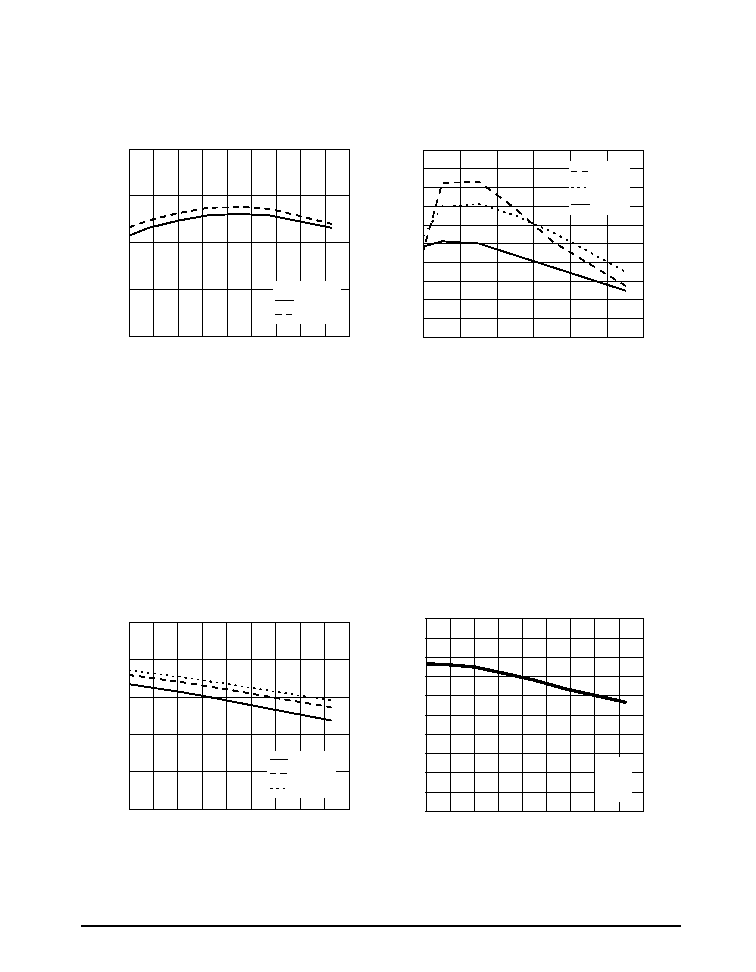
5
Date: 8/0/06 Rev G SP78MXX 500mA 3-Terminal Positive Voltage Regulator
© 2006 Sipex Corporation
Figure 6. Dropout Voltage vs. Junction Temperature
Typical Performance characteristics
Figure 5. Peak Output Current vs. Dropout Voltage
Figure 4. Output Voltage vs. Junction Temperature
-40
-20
0
20
40
60
80
100
120
140
4.90
4.95
5.00
5.05
5.10
O
u
t
p
u
t
V
o
l
t
a
g
e
(
V
)
Junction Temperature (
o
C)
SP78M05
I
OUT
=5mA
I
OUT
=500mA
-40
-20
0
20
40
60
80
100
120
140
0.0
0.5
1.0
1.5
2.0
2.5
D
r
o
p
o
u
t
V
o
l
t
a
g
e
(
V
)
Junction Temperature (
o
C)
I
OUT
=100mA
I
OUT
=350mA
I
OUT
=500mA
2
4
6
8
10
12
14
0.0
0.2
0.4
0.6
0.8
1.0
1.2
1.4
1.6
1.8
2.0
O
u
t
p
u
t
C
u
r
r
e
n
t
(
A
)
Dropout Voltage (V)
T
J
= -40
o
C
T
J
= 25
o
C
T
J
= 125
o
C
Figure 7. Quiescent Current vs. Junction Temperature
-40
-20
0
20
40
60
80
100
120
140
2.0
2.2
2.4
2.6
2.8
3.0
3.2
3.4
3.6
3.8
4.0
Q
u
i
e
s
c
e
n
t
C
u
r
r
e
n
t
(
m
A
)
Junction Temperature (
o
C)
S
P78M05
V
I N
=10V
I
OUT
=0