 | –≠–Ľ–Ķ–ļ—ā—Ä–ĺ–Ĺ–Ĺ—č–Ļ –ļ–ĺ–ľ–Ņ–ĺ–Ĺ–Ķ–Ĺ—ā: SP791 | –°–ļ–į—á–į—ā—Ć:  PDF PDF  ZIP ZIP |
1
SP791DS/08 SP791 Low Power Microprocessor Supervisory with Battery Switch-Over
© Copyright 2000 Sipex Corporation
s
Precision 4.65V Voltage Monitoring
s
200ms Power-OK/Reset Time Delay
s
Independent Watchdog Time-Preset or Adjustable
s
75
Ķ
A Maximum Operating Supply Current
s
1.0
Ķ
A Maximum Battery Backup Current
s
0.1
Ķ
A Maximum Battery Standby Current
s
Power Switching
250mA Output in Vcc Mode (0.6
)
25mA Output in Battery Mode (5
)
s
On-Board Gating of Chip-Enable Signals
Memory Write-Cycle Completion
6ns CE Gate Propagation Delay
s
Voltage Monitor for Power-Fail or Low Battery
s
Backup-Battery Monitor
s
RESET Valid to Vcc=1V
s
Pin Compatible Upgrade to MAX791
DESCRIPTION
The SP791 is a microprocessor (
Ķ
P) supervisory circuit that integrates a myriad of compo-
nents involved in discrete solutions to monitor power-supply and battery-control functions in
Ķ
P and digital systems. The SP791 offers complete
Ķ
P monitoring and watchdog functions.
The SP791 is ideal for a low-cost battery management solution and is well suited for portable,
battery-powered applications with its supply current of 40
Ķ
A. The 6ns chip-enable propaga-
tion delay, the 25mA current output in battery-backup mode, and the 250mA current output
in standard operation also makes the SP791 suitable for larger scale, high-performance
equipment.
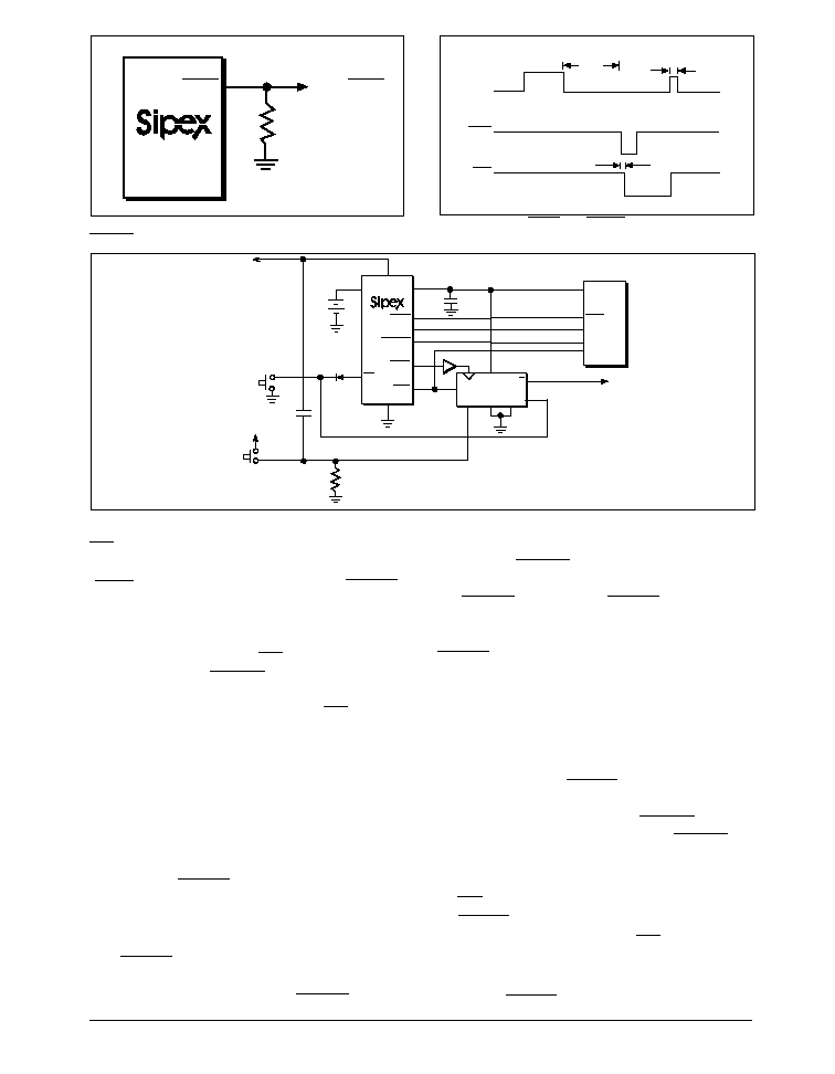
SP791
Figure 1. Block Diagram
150mV
4.65V
Vcc
V
BATT
CE
IN
13
1
3
LOWLINE
BATT ON
V
OUT
10
5
2
CE OUT
12
+
+
+
_
_
_
+
_
_
+
SP791
MR
SWT
WDI
PFI
1.25V
4
GND
7
11
8
9
RESET
WDPO
PFO
16
15
WDO
14
6
+
_
+
_
WATCHDOG
TIMER
V
OUT
TIMEBASE FOR
RESET AND
WATCHDOG
WATCHDOG
TRANSITION
DETECTOR
RESET
GENERATION
2V
CHIP-ENABLE
OUTPUT
CONTROL
Low Power Microprocessor Supervisory
with Battery Switch-Over
ģ
SP791DS/08 SP791 Low Power Microprocessor Supervisory with Battery Switch-Over
© Copyright 2000 Sipex Corporation
2
PARAMETER
MIN
TYP
MAX
UNITS
CONDITIONS
Operating Voltage Range
0
5.5
V
V
CC
, V
BATT
(Note 1)
V
CC
- 0.05 V
CC
- 0.015
V
CC
= 4.5V,
I
OUT
= 25mA
V
OUT
in Normal
V
CC
- 0.3
V
CC
- 0.15
V
V
CC
= 4.5V, I
OUT
= 250mA
Operating Mode
V
CC
- 0.2
V
CC
- 0.09
V
CC
=3.0V; V
BATT
= 2.8V, I
OUT
= 100mA
0.6
1.2
V
CC
=4.5V;
V
CC
-to-V
OUT
On Resistance
0.9
2.0
V
CC
=3.0V;
V
BATT
- 0.3
V
BATT
=4.5V, I
OUT
=20mA
V
OUT
in Battery Backup Mode
V
BATT
- 0.25
V
V
BATT
=2.8V, I
OUT
=10mA
V
BATT
- 0.15
V
BATT
=2.0V, I
OUT
=5mA
5
15
V
BATT
=4.5V
V
BATT
-to-V
OUT
On Resistance
7
25
V
BATT
=2.8V
10
30
V
BATT
=2.0V
Supply Current in Normal
Operating Mode (Excludes I
OUT
)
40
75
Ķ
A
V
CC
> V
BATT
≠ 1V
Supply Current in Battery Backup
0.001
1
Ķ
A
V
CC
< V
BATT
≠ 1.2V ; V
BATT
= 2.8V
Mode (Excludes I
OUT
) (Note 2)
V
BATT
Standby Current
-0.1
0.02
Ķ
A
V
BATT
+ 0.2V < V
CC
(Note 3)
Battery-Switchover Threshold
V
BATT
+0.03
Power up
V
BATT
-0.03
V
Power down
Battery-Switch over Hysteresis
60
mV
Peak to Peak
Low-Battery Detector Threshold
2
V
ABSOLUTE MAXIMUM RATINGS
Input Voltage (with respect to GND)
VCC..................................................-0.3V to +6V
VBATT.................................. ............-0.3V to +6V
All Other Inputs ................-0.3V to (VOUT + 0.3V)
Input Current
VCC Peak..................................................... 1.0A
VCC Continuous .......................................250mA
VBATT Peak ..............................................250mA
VBATT Continuous.......................................25mA
GND, BATT ON .........................................100mA
All Other Outputs ........................................25mA
Continuous Power Dissipation (TA = + 70
o
C)
Plastic DIP (derate 10.53mW/
o
C above +70
o
C)
842mW
Narrow SO (derate 8.70mW/
o
C above+70
o
C)
696mW
ESD Rating........................................................4KV
ELECTRICAL CHARACTERISTICS
(Vcc = 4.75V to 5.5V, V
BATT
= 2.8V, T
A
= T
MIN
to T
MAX
unless otherwise noted, typicals specified at 25
o
C)
Stresses beyond these listed under "Absolute Maximum
Ratings" may cause permanent damage to the device. These
are stress ratings only, and functional operation of the de-
vice at these or any other conditions beyond those indi-
cated in the operational sections of the specifications is
not implied. Exposure to absolute maximum rating condi-
tions for extended periods may affect device reliability.
Operating Temperature Ranges
SP791C ..............................0
o
C to +70
o
C
SP791E ...........................-40
o
C to +85
o
C
Storage Temperature Range...........-65
o
C to +160
o
C
Lead Temperature (soldering,10sec)..........+300
o
C
3
SP791DS/08 SP791 Low Power Microprocessor Supervisory with Battery Switch-Over
© Copyright 2000 Sipex Corporation
ELECTRICAL CHARACTERISTICS (continued)
(Vcc = 4.75V to 5.5V, V
BATT
= 2.8V, T
A
= T
MIN
to T
MAX
unless otherwise noted, typicals specified at 25
o
C)
PARAMETER
MIN
TYP
MAX
UNITS
CONDITIONS
BATT ON Output
0.1
0.4
V
I
SINK
= 3.2mA
Low Voltage
0.7
1.5
I
SINK
= 25mA
BATT ON Output
60
mA
Sink Current
Short Circuit Current
1
15
100
Ķ
A
Source Current
RESET, LOW-LINE AND WATCHDOG TIMER
RESET Threshold Voltage
4.50
4.65
4.75
V
RESET Threshold Hysteresis
15
mV
LOWLINE-to-RESET
150
mV
Threshold Voltage
V
CC
-to-RESET Delay
100
Ķ
s
Power down
V
CC
-to-LOWLINE Delay
80
Ķ
s
Power down
RESET Active Timeout Period
140
200
280
ms
Power up
Watchdog Timeout Period
1.0
1.6
2.25
sec
SWT connected to V
OUT
Minimum Watchdog
10
ms
4.7nF capacitor connected from
Timeout Period
SWT to GND
Minimum Watchdog Input
100
ns
V
IL
= 0.8V, V
IH
= 0.75 X V
CC
Pulse Width
WDPO Pulse Width
1
ms
WDPO-to-WDO Delay
70
ns
RESET Output Voltage
0.004
0.3
V
I
SINK
=50
Ķ
A,V
CC
=1.0V,V
CC
ń
0.1
0.4
I
SINK
= 3.2 mA, V
CC
= 4.25V
3.5
I
SOURCE
= 1.6mA, V
CC
= 5V
RESET Output
Short-Circuit Current
7
20
mA
Output source current
LOWLINE Output Voltage
0.4
V
I
SINK
= 3.2mA, V
CC
= 4.25V
3.5
I
SOURCE
= 1
Ķ
A, V
CC
= 5V
LOWLINE Output
15
100
Ķ
A
Output source current
Short-Circuit Current
WDO Output Voltage
0.4
V
I
SINK
= 3.2mA
3.5
I
SOURCE
= 500
Ķ
A, V
CC
= 5V
WDO Output Short-Circuit
3
10
mA
Output source currrent
Current
WDPO Output Voltage
0.4
V
I
SINK
= 3.2mA
3.5
I
SOURCE
= 1mA
WDPO Output Short-Circuit
7
20
mA
Output source current
Current
SP791DS/08 SP791 Low Power Microprocessor Supervisory with Battery Switch-Over
© Copyright 2000 Sipex Corporation
4
PARAMETER
MIN
TYP
MAX
UNITS
CONDITIONS
WDI Threshold Voltage
0.75 X V
CC
V
V
IH
(Note 4)
0.8
V
IL
WDI Input Current
-50
-10
Ķ
A
WDI = 0V
20
50
WDI = V
OUT
POWER FAIL COMPARATOR
PFI Input Threshold
1.20
1.25
1.30
V
V
CC
= 5V
PFI Leakage Current
+0.01
+25
nA
PFO Output Voltage
0.4
V
I
SINK
= 3.2mA
3.5
I
SOURCE
= 1
Ķ
A, V
CC
= 5V
PFO Short-Circuit Current
60
mA
Output sink current
1
15
100
Ķ
A
Output source current
PFI-to-PFO Delay
15
Ķ
s
V
OD
= 15mV
55
V
OD
= 15mV
CHIP-ENABLE GATING
CE
IN
Leakage Current
+0.005
+1
Ķ
A
Disabled mode
CE
IN
-to-CE
OUT
Resistance
65
150
Enabled mode
(Note 5)
CE
OUT
Short-Circuit Current
0.1
0.75
2.0
mA
Disabled mode, CE OUT = 0V
(Reset Active)
CE
IN
-to-CE
OUT
Propagation
6
10
ns
50
source impedance driver,
Delay (Note 6)
C
LOAD
= 50pF
CE
OUT
Output Voltage High
3.5
V
V
CC
= 5V, I
OUT
= 100
Ķ
A
(Reset Active)
2.7
V
CC
= 0V, V
BATT
= 2.8V, I
OUT
= 1
Ķ
A
RESET-to-CE
OUT
Delay
15
Ķ
s
Power down
MANUAL RESET INPUT
MR Minimum Pulse Width
25
15
Ķ
s
MR-to-RESET
7
Ķ
s
Propagation Delay
MR Threshold
1.25
V
V
CC
= 5V
MR Pull-Up Current
23
250
Ķ
A
MR = 0V
Note 1:
Either V
CC
or V
BATT
can go to 0V, if the other is
greater than 2.0V.
Note 2:
The supply current drawn by the SP791 from the
battery (excluding I
OUT
) typically goes to 10
Ķ
A when (V
BATT
- 1V) < V
CC
< V
BATT
. In most applications, this is a brief
period as V
CC
falls through this region.
Note 3:
"+" = battery-discharging current,
"-" = battery-charging current.
Note 4:
WDI is internally connected to a voltage divider
between V
OUT
and GND. If unconnected, WDI is driven to
1.6V (typ), disabling the watchdog function
.
ELECTRICAL CHARACTERISTICS (continued)
(Vcc = 4.75V to 5.5V, V
BATT
= 2.8V, T
A
= T
MIN
to T
MAX
unless otherwise noted, typicals specified at 25
o
C)
Note 5:
The chip-enable resistance is tested with V
CC
=
4.75V :: V
CE IN
= V
CE
OUT
=V
CC
/2
.
Note 6:
The chip-enable propagation delay is measured
from the 50% point at CE IN to the 50% point at CE
OUT
.
5
SP791DS/08 SP791 Low Power Microprocessor Supervisory with Battery Switch-Over
© Copyright 2000 Sipex Corporation
to select another watchdog-timeout period.
Watchdog-timeout period = 2.1 x (capacitor
value in nF) ms.
Pin 9 -- MR -- Manual-Reset Input. This input
can be tied to an external momentary
pushbutton switch, or to a logic gate output.
RESET remains low as long as MR is held
low and for 200ms after MR returns high.
Pin 10 -- LOWLINE -- LOWLINE Output goes
low when V
CC
falls to 150mV above the re-
set threshold. The output can be used to gen-
erate an NMI (nonmaskable interrupt) if the
unregulated supply is inaccessible.
Pin 11 -- WDI -- Watchdog Input. WDI is a three-
level input. If WDI remains either high or
low for longer than the watchdog timeout
period, WDO goes low. WDO remains low
until the next transition at WDI. Leaving
WDI unconnected disables the watchdog
function. WDI connects to an internal volt-
age divider between V
OUT
and GND, which
sets it to mid-supply when left unconnected.
Pin 12 -- CE
OUT
-- Chip-Enable Output.
CE
OUT
goes low only when CE
IN
is low
and V
CC
is above the reset threshold. If CE
IN
is low when reset is asserted, CE
OUT
will
stay low for 15us or until CE
IN
goes high,
whichever occurs first.
Pin 13 -- CE
IN
-- Chip-Enable Input. The Input
to chip-enable gating circuit. Connect to
GND or V
OUT
if not used.
Pin 14 -- WDO -- Watchdog Output. WDO goes
low if WDI remains either high or low longer
than the watchdog timeout period. WDO
returns high on the next transition at WDI.
WDO remains high if WDI is unconnected.
WDO is also high when RESET is asserted.
Pin 15 -- RESET -- RESET Output goes low
whenever V
CC
falls below the reset thresh-
old. RESET will remain low for 200ms
after V
CC
crosses the reset threshold on
power-up.
Pin 16 -- WDPO -- Watchdog-Pulse Output.
Upon the absence of a transition at WDI,
WDPO will pulse low for a minimum of
1ms. WDPO precedes WDO by 70ns.
PIN ASSIGNMENTS
Pin 1 -- V
BATT
-- Backup-Battery Input. Connect
to external battery or capacitor and charging
circuit.
Pin 2 --V
OUT
-- Output Supply Voltage. V
OUT
con-
nects to V
CC
when V
CC
is greater than V
BATT
and V
CC
is above the reset threshold. When
V
CC
falls below V
BATT
and V
CC
is below the
reset threshold, V
OUT
connects to V
BATT
. Con-
nect a 0.1
Ķ
F capacitor from V
OUT
to GND.
Pin 3 -- V
CC
-- Input Supply Voltage --
+5V input
Pin 4 -- GND -- Ground reference for all signals
Pin 5 -- BATT ON -- Battery On Output. Goes
high when V
OUT
switches to V
BATT
. Goes low
when V
OUT
switches to V
CC
. Connect the base
of a PNP through a current-limiting resistor
to BATT ON for V
OUT
current requirements
greater than 250mA.
Pin 6 -- PFO -- Power-Fail Output. This is the
output of the power-fail comparator. PFO
goes low when PFI is less than1.25V. This is
an uncommitted comparator, and has no ef-
fect on any other internal circuitry.
Pin 7 -- PFI -- Power-Fail Input. This is the
noninverting input to the power-fail compara-
tor. When PFI is less than 1.25V, PFO goes
low. Connect PFI to GND or V
OUT
when not
used.
Pin 8 -- SWT -- Set Watchdog-Timeout Input.
Connect this input to V
OUT
to select the de-
fault 1.6 sec watchdog timeout period. Con-
nect a capacitor between this input and GND
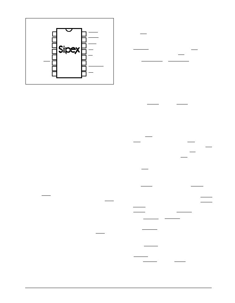
PINOUT
V
BATT
V
OUT
Vcc
GND
BATT ON
PFO
PFI
SWT
WDPO
RESET
WDO
CE
IN
CE
OUT
WDI
LOWLINE
MR
16
DIP/SO
TOP VIEW
15
14
13
12
11
10
9
1
2
3
4
5
6
7
8
Corporation
SP791DS/08 SP791 Low Power Microprocessor Supervisory with Battery Switch-Over
© Copyright 2000 Sipex Corporation
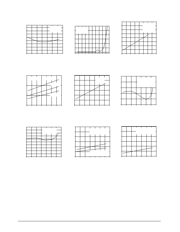
6
-60 -30 0 30
60 90 120 150
Temperature Deg. C
V
CC
Supply Current vs.
Temperature (Normal Mode)
Battery Supply Current vs.
Temperature (Backup Mode)
Chip Enable On
Resistance vs. Temperature
V
BATT
to V
OUT
ON
Resistance vs. Temperature
V
CC
to V
OUT
On
Resistance vs. Temperature
PFI Threshold
vs. Temperature
Reset Threshold
vs. Temperature
Reset Output Resistance
vs. Temperature
Reset Delay
vs. Temperature
57
53
49
45
41
37
33
29
25
-60 -30 0 30
60 90 120 150
V
CC
Current (
Ķ
A)
Temperature Deg. C
2.9
2.4
1.9
1.4
0.9
0.4
-0.1
V
BATT
Current (
Ķ
A)
-60
Temperature Deg. C
-40 -20
0 20 40 60 80 100 120 140
120
110
100
90
80
70
60
50
40
Resistance (ohms)
-60 -30 0 30 60 90 120 150 180
Temperature Deg. C
15
10
5
0
Resistance (ohms)
-60 -30 0 30
60 90 120 150
Temperature Deg. C
0.9
0.8
0.7
0.6
0.5
0.4
0.3
Resistance (ohms)
-60 -30 0 30
60 90 120 150
Temperature Deg. C
1.256
1.254
1.252
1.250
1.248
1.246
PFI Threshold (V)
4.70
4.69
4.68
4.67
4.66
4.65
4.64
4.63
4.62
4.61
4.60
Reset Threshold (V)
-60 -30 0 30
60 90 120 150
Temperature Deg. C
600
500
400
300
200
100
0
Resistance (ohms)
-60 -30 0 30
60 90 120 150
Temperature Deg. C
212
210
208
206
204
202
200
Reset Delay (mS)
-60 -30 0 30
60 90 120 150
Temperature Deg. C
V
CC
=5V
V
BATT
=2.8V
V
CC
=0V
V
BATT
=2.8V
V
CC
=4.75V
V
BATT
=2.8V
CE IN=V
CC
/2
V
BATT
=2.8V
V
BATT
=4.5V
V
CC
=5V
V
BATT
=0V
V
CC
=5V
V
BATT
=0
NO LOAD ON PFO
V
BATT
=0V
Power Down
V
CC
=5V,V
BATT
=2.8V
Soucing Current
V
CC
=0V to 5V Step,
V
BATT
=2.8V
TYPICAL CHARACTERISTICS
(25
o
C, unless otherwise noted)
V
CC
=0V,V
BATT
=2.8V
Sink Current
V
CC
=0V V
BATT
=2V
7
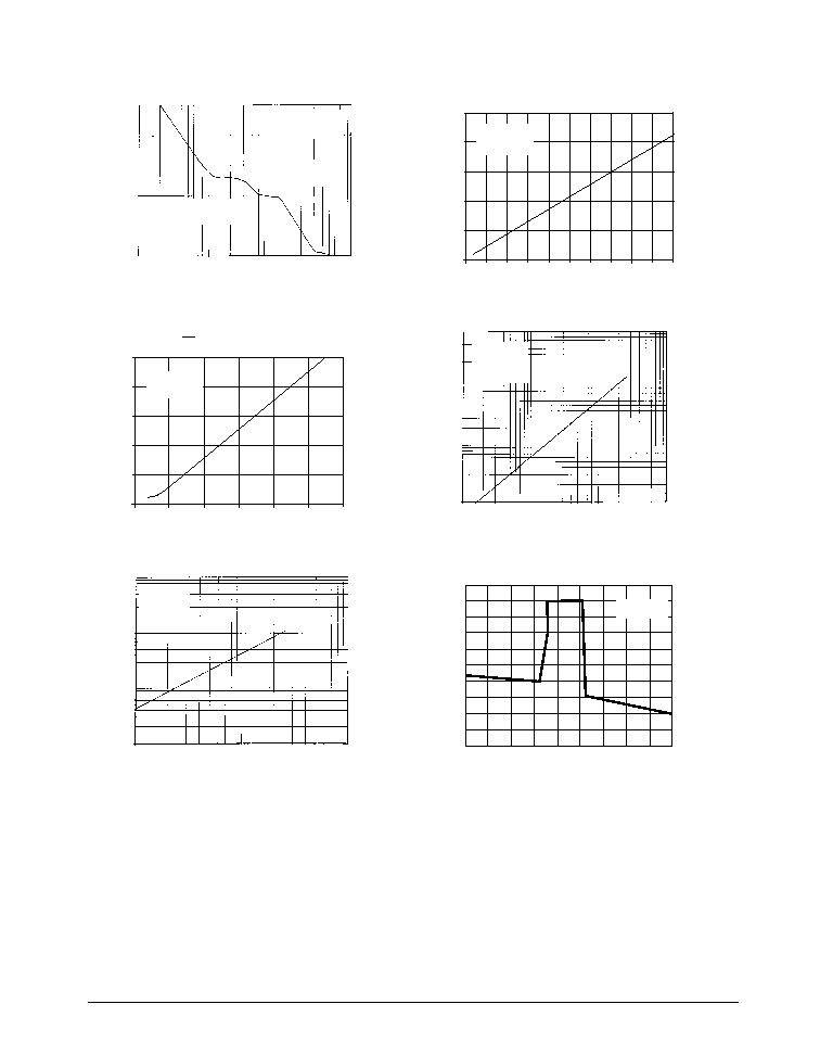
SP791DS/08 SP791 Low Power Microprocessor Supervisory with Battery Switch-Over
© Copyright 2000 Sipex Corporation
Maximum Reset Comparator Overdrive
Without Causing a Reset
100
80
60
40
20
0
Maximum Transient Duration (uS)
10 100 1000 10000
Watchdog Timeout
vs. Timing Capacitor
250
200
150
100
50
0
Watchdog Tiimeout (mS)
0 10 20 30 40 50 60 70 80 90 100
Timing Capacitor (nF)
Chip-Enable Propagation Delay
vs. CE OUT Load Capacitance
20
16
12
8
4
0
Propagation Delay (NS)
0 50 100 150 200 250 300
Cload (pF)
V
CC
to V
OUT
vs.
Output Current
1000
100
10
1
Voltage Drop(mV)
1 10 100 1000
IOUT (mA)
VBATT to VOUT vs.
Output Current
1000
100
10
1
Voltage Drop(mV)
1 10 100
IOUT (mA)
IE+2
IE+1
IE+0
IE-1
IE-2
IE-3
IE-4
IE-5
IE-6
IE-7
IE-8
V
BATT
Current(
Ķ
A) Log Scale
.0000 5.000
V
CC
(0.5V/div)
Battery Current vs. V
CC
Voltage
V
CC
=4.5V
V
BATT
=0V
Slope=0.6
V
BATT
=4.5V
V
CC
=0V
Slope=5
V
BATT
=2.8V
TYPICAL CHARACTERISTICS
(25
o
C, unless otherwise noted)
Reset Threshold Voltage - V
CC
(mV)
0.1
Ķ
F Capacitor
V
OUT
to GND
Above Line
Reset Generated
Below Line
No Reset Generated
V
CC
=5V
V
BATT
=2.8V
VCC=5V
50
Driver
SP791DS/08 SP791 Low Power Microprocessor Supervisory with Battery Switch-Over
© Copyright 2000 Sipex Corporation
8
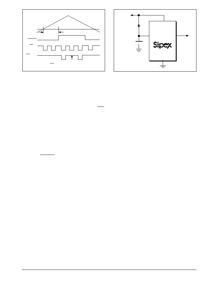
2) Manual-Reset input ¨ Manually resets
RESET output
3) Power Fail Comparator ¨ Provides for power-
fail warning and low-battery detection, or
monitors another power supply.
4) Watchdog function ¨ Monitors
Ķ
P activity
where the watchdog output goes to a logic
LOW state if the watchdog input is not toggled
for a period greater than the timeout period.
5) Internal switch ¨ Switches over from V
CC
to
V
BATT
if the V
CC
falls below the reset thresh-
old and below V
BATT
.
MANUAL RESET INPUT
Many microprocessor or microcontroller prod-
ucts include manual-reset capability, allowing
the operator or test technician to initiate a reset.
The Manual Reset Input (MR) can be connected
directly to a switch, without an external pull-up
resistor. It connects to a 1.25V comparator, and
has an internal pull-up to V
OUT
as shown in Fig-
ure 1. The propagation delay from asserting MR
to RESET being asserted is 7us typical. Pulsing
FEATURES
The SP791 is a microprocessor (
Ķ
P) supervi-
sory circuit that monitors the power supplied to
digital circuits such as microprocessors,
microcontrollers, or memory. The SP791 is an
ideal solution for portable, battery-powered
equipment that require power supply monitor-
ing. The SP791 watchdog functions will con-
tinuously oversee the operational status of a sys-
tem. Implementing the SP791 will reduce the
number of components and overall complexity
in a design that requires power supply monitor-
ing circuitry. The operational features and ben-
efits of the SP791 are described in more detail
below.
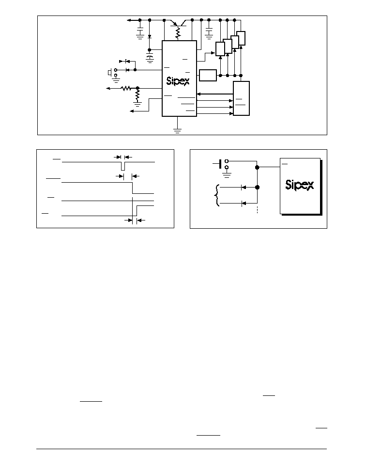
THEORY OF OPERATION
The SP791 is a complete
Ķ
P supervisor IC and
provides the following main functions:
1)
Ķ
P reset ¨ RESET output is asserted during
power fluctuations such as power-up, power-
down, and brown out conditions, and is guar-
anteed to be in the correct state for V
CC
down
to 1V.
Figure 2. Manual-Reset Timing Diagram
Typical Operating Circuit
Figure 3. Diode "OR" connections allow multiple reset
sources to connect to MR.
Corporation
V
cc
BATT
ON
SWT
V
OUT
CE
OUT
MR
CE
IN
PFI
PFO
GND
WDI
LOWLINE
RESET
WDO
UNREGULATED
SUPPLY FAILURE
OTHER SYSTEM
RESET SOURCES
0.47F
ADDRESS
DECODE
0.1
Ķ
F
+5V
0.1
Ķ
F
CMOS
RAM
AO-A15
Ķ
P
I/O
NMI
RESET
INT
V
BATT
UNREGULATED
SUPPLY
MANUAL RESET
OTHER
RESET
SOURCES
*
DIODES NOT REQUIRED ON OPEN-DRAIN OUTPUTS
*
*
MR
Corporation
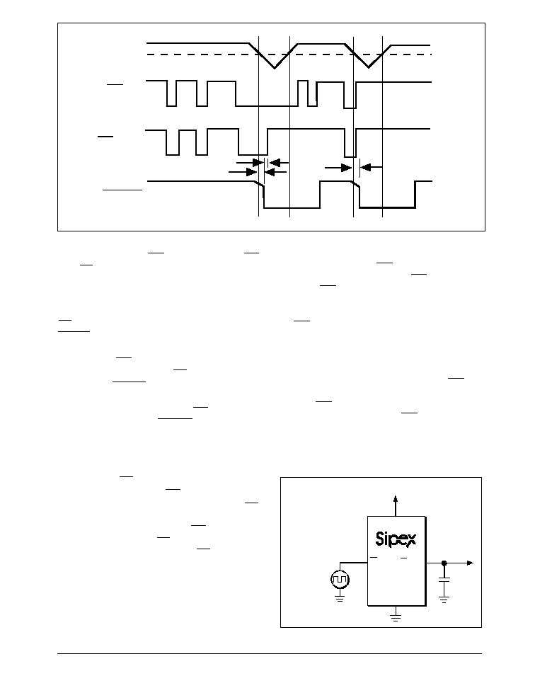
MR
RESET
CE
IN
0V
CE
OUT
25
Ķ
s MIN
7
Ķ
s TYP
15
Ķ
s TYP
9
SP791DS/08 SP791 Low Power Microprocessor Supervisory with Battery Switch-Over
© Copyright 2000 Sipex Corporation
MR low for a minimum of 25
Ķ
s resets all the
internal counters, sets the Watchdog Output
(WDO) and Watchdog-Pulse Output (WDPO)
high, and sets the Set Watchdog-Timeout (SWT)
input to V
OUT
if it is not already connected to
V
OUT
(for Internal timeouts). It also, disables
the Chip-Enable Output (CE
OUT
) forcing it to
a high state. The RESET output remains at a
logic low as long as MR is held low, and the
reset-timeout period begins after MR returns
high, Figure 2.
Use this input as either a digital-logic input or a
second low-line comparator. Normal TTL/
CMOS levels can be wire-OR connected via
pull-down diodes, Figure 3, and open-drain/col-
lector outputs can be wire-ORed directly.
RESET OUTPUT
The SP791's RESET output ensures that the
Ķ
P
powers up in a known state, and prevents code-
execution errors during power-down or brown-
out conditions.
The RESET output is active low, and typically
sinks 3.2mA at 0.1V saturation voltage in its
active state. When deasserted, RESET sources
1.6mA at V
OUT
≠ 0.5V. When no backup bat-
tery is used, RESET output is valid down to V
CC
= 1V, and an external 10k
pull-down resistor
on RESET ensures that RESET will be valid
with V
CC
down to GND as shown on Figure 4.
As V
CC
goes below 1V, the gate drive to the
RESET output switch reduces accordingly,
increasing the r
DS
(ON) and the saturation volt-
age. The 10k
pull-down resistor ensures the
parallel combination of switch and external
resistor is 10k
and the output saturation volt-
age is below 0.4V, while sinking 40
Ķ
A. When
using a 10k
external pull-down resistor, the
high state for the RESET output with Vcc =
4.75V is 4.5V typical. For battery voltages
greater than or equal to 2V, RESET remains
valid for V
CC
between 0V and 5.5V. RESET will
be asserted during the following conditions:
1) V
CC
< 4.65V (typ)
2) MR < 1.25V (typ)
3) RESET = logic "0" ; for 200 ms (typ) after
Vcc rises above 4.65V or after MR has exceeded
1.25V.
The SP791 battery-switchover comparator does
not affect RESET assertion.
Figure 5. WDI, WDO and WDPO Timing
Diagram (V
CC
mode).
Figure 4. Adding an external pull-down resistor ensures
RESET is valid with V
CC
down to GND.
Figure 6. Two consecutive watchdog faults latch the system in reset.
TO
Ķ
P RESET
10k
15
Corporation
RESET
1.6sec
100ns MIN
WDI
WDPO
WDO
70ns
Corporation
Vcc
V
BATT
V
OUT
RESET
WDI
LOWLINE
WDPO
WDO
GND
MR
3.6V
1
3
2
15
11
10
16
14
9
4.7k
*
1
Ķ
F
+5V
REACTIVATE
4
CLOCK
D
SET
Vcc
CD4013
RESET
Vss
Q
Q
2
1
14
3
6
5
4
7
1/6 74HC04
TWO
CONSECUTIVE
WATCHDOG
FAULT
INDICATIONS
Ķ
P POWER
Ķ
P
RESET
I/O
NMI
INTERRUPT
0.1
Ķ
F
+5V
SETS Q HIGH ON POWER-UP

SP791DS/08 SP791 Low Power Microprocessor Supervisory with Battery Switch-Over
© Copyright 2000 Sipex Corporation
10
WATCHDOG FUNCTION
The watchdog monitors
Ķ
P activity via the
Watchdog Input (WDI). If the
Ķ
P becomes in-
active over a period of time, WDO and WDPO
are asserted
.
To use the watchdog functon, connect WDI to a
bus line or
Ķ
P I/O line. If WDI remains high or
low for longer than the watchdog timeout
period (1.6sec nominal), WDPO and WDO are
asserted, indicating a software fault or idle
condition.
WATCHDOG INPUT
A change of logic state (minimum 100ns dura-
tion) at WDI during the watchdog period will
reset the watchdog timer. The watchdog default
timeout is 1.6sec. To select an alternative
timeout period, connect an external capacitor
from SWT to GND.
To disable the watchdog function, leave WDI
floating. An internal impedance network (100k
equivalent at WDI) biases WDI to approximately
1.6V. Internal comparators detect this level and
disable the watchdog timer. When Vcc is below
the reset threshold, the watchdog function is dis-
abled and WDI is disconnected from its internal
network, thus becoming high impedance.
WATCHDOG OUTPUT
WDO remains high if there is activity (transi-
tion or pulse) at WDI during the watchdog-
timeout period. The watchdog function is dis-
abled and WDO is a logic high when V
CC
is
less than the reset threshold, or when WDI is an
open circuit. In watchdog mode, if no transi-
tion occurs at WDI during the watchdog-timeout
period, WDO goes low 70ns after the falling
edge of WDPO and remains low until the next
transition at WDI as shown on Figure 5. A flip-
flop can force the system into a hardware shut-
down if there are two successive watchdog
faults, shown on Figure 6. WDO has a 2 x TTL
output characteristic.
WATCHDOG-PULSE OUTPUT
As described in the preceding section, WDPO
can be used as the clock input to an external D
flip-flop. Upon the absence of a watchdog edge
or pulse at WDI at the end of a watchdog-timeout
period, WDPO will pulse low for 1ms. The fall-
ing edge of WDPO precedes WDO by 70ns.
Since WDO is high when WDPO goes low, the
Q output of the flip-flop remains high as WDO
goes low (Figure 6). If the watchdog timer is
not reset by a transition at WDI, WDO remains
low and WDPO clocks a logic low to the Q out-
put, causing the SP791 to latch in reset. If the
watchdog timer is reset by a transition at WDI,
WDO goes high and the flip-flop's Q output re-
mains high. Thus, a system shutdown is only
caused by two successive watchdog faults.
The internal pull-up resistors associated with
WDO and WDPO connect to V
OUT
. Therefore,
do not connect these outputs directly to CMOS
logic that is powered from V
CC
since, in the ab-
sence of V
CC
(i.e., battery mode), excessive
current will flow from WDO or WDPO through
the protection diode(s) of the CMOS-logic in-
puts to ground.
SELECTING AN ALTERNATIVE
WATCHDOG TIMEOUT PERIOD
SWT input controls the watchdog-timeout pe-
riod. Connecting SWT to V
OUT
selects the in-
ternal 1.6sec watchdog-timeout period. Select
an alternative timeout period by connecting a
capacitor between SWT and GND. Do not leave
SWT floating, and do not connect it to ground.
The following formula determines the watch-
dog-timeout period:
Watchdog Timeout Period = 2.1 x
(capacitor value in nF) ms
This formula is valid for capacitance values
between 4.7 nF and 100nF (see the Watchdog
Timeout vs. Timing Capacitor graph in the Typi-
cal Operating Characteristics).
CHIP-ENABLE SIGNAL GATING
The SP791 provides internal gating of chip-en-
able (CE) signals to prevent erroneous data from
corrupting the CMOS RAM in the event of a
power failure. During normal operation, the CE
gate is enabled and passes all CE transitions.
When reset is asserted, this path becomes dis-
abled, preventing erroneous data from corrupt-
ing the CMOS RAM. The SP791 uses a series
transmission gate from CE
IN
to CE
OUT
.
11
SP791DS/08 SP791 Low Power Microprocessor Supervisory with Battery Switch-Over
© Copyright 2000 Sipex Corporation
The 10ns maximum CE propagation from CE
IN
to CE
OUT
enables the SP791 to be used with
most
Ķ
Ps.
CHIP-ENABLE INPUT
CE
IN
is high impedance (disabled mode) while
RESET is asserted.
During a power-down sequence where V
CC
falls
below 4.65V, CE IN assumes a high impedance
state when the voltage at CE
IN
goes high or
15
Ķ
s after RESET is asserted, whichever
occurs first, (Figure 7).
During a power-up sequence, CE
IN
remains
high impedance until RESET is deasserted.
In the high-impedance mode, the leakage
currents into this input are less than 1
Ķ
A over
temperature. In the low-impedance mode, the
impedance of CE
IN
appears as a 65
resistor
in series with the load at CE
OUT
.
The propagation delay through the CE
transmission gate depends on both the source
impedance of the drive to CE
IN
and the
capacitive loading on CE
OUT
(see the Chip-
Enable Propagation Delay vs. CE
OUT
Load
Capacitance graph in the Typical Operating
Characteristics). The CE propagation delay is
defined from the 50% point on CE
IN
to the 50%
point on CE
OUT
using a 50
driver with 50pF
load capacitance as in Figure 8. For minimum
propagation delay, minimize the capacitive load
at CE
OUT
and use a low output-impedance
driver.
CHIP-ENABLE OUTPUT
In the enabled mode, the impedance of CE
OUT
is equivalent to 65
in series with the source
driving CE
IN
. In the disabled mode, the 65
transmission gate is off and CE
OUT
is actively
pulled to V
OUT
. This source turns off when the
transmission gate is enabled.
Figure 8. CE Propagation Delay Test Circuit
Figure 7. Reset and Chip-Enable Timing
+5V
Vcc
50
Driver
GND
CE
IN
CE
OUT
50pF
C
LOAD
Corporation
Vcc
CE
IN
CE
OUT
RESET
15
Ķ
s
100
Ķ
s
100
Ķ
s
RESET
THRESHOLD
SP791DS/08 SP791 Low Power Microprocessor Supervisory with Battery Switch-Over
© Copyright 2000 Sipex Corporation
12
POWER-FAIL INPUT
The Power-Fail Input (PFI) has a guaranteed
input leakage of +/-25nA max over temperature.
The typical comparator delay is 15
Ķ
s from V
IL
to V
OL
(power failing), and 55
Ķ
s from V
IH
to
V
OH
(power being restored). Connect PFI to
ground if not used.
POWER-FAIL OUTPUT
The Power-Fail Output (PFO) goes low when
PFI falls below 1.25V. It sinks 3.2mA with a
saturation voltage of 0.1V. With PFI above
1.25V, PFO is actively pulled to V
OUT
. Con-
necting PFI through a voltage divider to an un-
regulated supply allows PFO to generate an NMI
as the unregulated power begins to fall (see
Figure 9b).
LOWLINE OUTPUT
The low-line comparator monitors V
CC
with a
typical threshold voltage 150mV above the re-
set threshold and has 15mV of hysteresis.
LOWLINE typically sinks 3.2mA at 0.1V. For
normal operation (Vcc above the LOWLINE
threshold), LOWLINE is pulled to V
OUT
. If ac-
cess to the unregulated supply is unavailable,
use LOWLINE to provide a nonmaskable in-
terrupt (NMI) to the
Ķ
P as shown in Figure 9a.
POWER-FAIL COMPARATOR
The power-fail comparator is an uncommitted
comparator that has no effect on the other func-
tions of the SP791. Common uses include moni-
toring supplies other than 5V (see the Typical
Operating Circuit and the Monitoring a Nega-
tive Voltage section) and early power-fail de-
tection when the unregulated power is easily ac-
cessible as shown in Figure 9b.
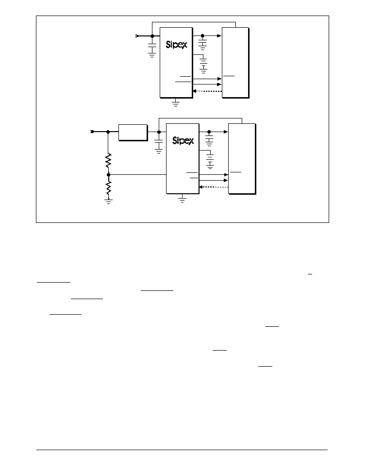
Figure 9. a) If the unregulated supply is inaccessible, LOWLINE generates the NMI for the
Ķ
P.
b) Use PFO to generate the
Ķ
P NMI if the unregulated supply is accessible.
FROM
REGULATED
SUPPLY
0.1
Ķ
F
3
2
1
15
10
11
0.1
Ķ
F
3.0V
4
POWER TO
CMOS RAM
Ķ
P
RESET
RESET
NMI
LOWLINE
I/O LINE
WDI
GND
V
BATT
V
OUT
Vcc
Corporation
UNREGULATED
SUPPLY
a.)
b.)
Ķ
P POWER
3
2
1
15
6
11
0.1
Ķ
F
3.0V
4
POWER TO
CMOS RAM
Ķ
P
RESET
RESET
NMI
PFO
I/O LINE
WDI
GND
V
BATT
V
OUT
Vcc
Corporation
Ķ
P POWER
PFI
7
0.1
Ķ
F
VOLTAGE
REGULATOR
13
SP791DS/08 SP791 Low Power Microprocessor Supervisory with Battery Switch-Over
© Copyright 2000 Sipex Corporation
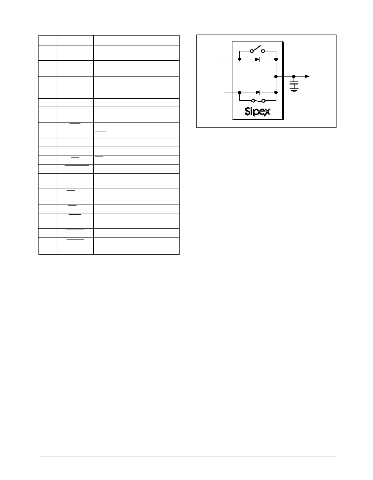
PIN
NAME
STATUS
1
V
BATT
Supply current is 1
Ķ
A maximum
When V
CC
< V
BATT
-1.2V
2
V
OUT
V
OUT
is connected to V
BATT
through an Internal PMOS switch.
3
V
CC
Battery-switchover comparator
monitors V
CC
for active switchover.
V
CC
is disconnected from V
OUT
4
GND
GND-0V reference for all signals.
5
BATT ON
Logic high. The open-circuit output is
equal to V
OUT
.
6
PFO
The power-fail comparator is disabled
PFO is forced low.
7
PFI
The power-fail comparator is disabled
8
SWT
SWT is Ignored.
9
MR
MR is ignored.
10
LOWLINE Logic low.
11
WDI
WDI is ignored, and goes high
impedance.
12
CE
OUT
Logic high. The open-circuit output
voltage is equal to V
OUT
.
13
CE
IN
High Impedance.
14
WDO
Logic high. The open-circuit output
voltage is equal to V
OUT
.
15
RESET Logic low.
16
WDPO
Logic high. The open-circuit output
voltage is equal to V
OUT
.
INPUT SUPPLY VOLTAGE
The Input Supply Voltage (V
CC
) should be a
regulated +5V source. V
CC
connects to V
OUT
via a parallel diode and a large PMOS switch
(Figure 10). The switch carries the entire
current load for currents less than 250mA.
The parallel diode carries any current in excess
of 250mA. The maximum continuous current
is 250mA, but power-on transients may reach a
maximum of 1A.
BACKUP-BATTERY INPUT
The Backup-Battery Input (V
BATT
) is similar
to V
CC
, except the PMOS switch and parallel
diode are much smaller. Continuous current
should be limited to 25mA and peak currents
(only during power-up) limited to 250mA. The
reverse leakage of this input is less than 1
Ķ
A
over temperature and supply voltage.
OUTPUT SUPPLY VOLTAGE
The Output Supply Voltage (V
OUT
) supplies all
the current to the external system and internal
circuitry. All open-circuit outputs will, for ex-
ample, assume the V
OUT
voltage in their high
states rather than the V
CC
voltage. At the maxi-
mum source current of 250mA, V
OUT
will typi-
cally be 200mV below V
CC
. V
OUT
should be
decoupled with 0.1
Ķ
F capacitor.
BATTERY-BACKUP MODE
The SP791 requires two conditions to switch to
battery-backup mode: 1) V
CC
must be below
the reset threshold; 2) V
CC
must be below
V
BATT
. Table 1 lists the status of the inputs and
outputs in battery-backup mode.
BATTERY ON OUTPUT
The Battery On Output (BATT ON) indicates
the status of the internal V
CC
/battery-switchover
comparator, which controls the internal V
CC
and
V
BATT
switches. For V
CC
greater than V
BATT
(ignoring the small hysteresis effect), BATT ON
is a logic low. For V
CC
less than V
BATT
, BATT
ON is a logic high. Use BATT ON to indicate
battery-switchover status or to supply base drive
to an external pass transistor for higher-current
applications (see Typical Operating Circuit).
Figure 10. V
CC
and V
BATT
-to-V
OUT
Switch
To enter the Battery-Backup mode, V
CC
must be less than
the Reset threshold and less than V
BATT
.
Table 1. Input/Output states in Battery-Backup mode
Corporation
V
BATT
Vcc
2
V
OUT
0.1
Ķ
F
INPUT/OUTPUT STATES IN
BATTERY-BACKUP MODE
SP791DS/08 SP791 Low Power Microprocessor Supervisory with Battery Switch-Over
© Copyright 2000 Sipex Corporation
14
There are three distinct modes of operation:
1) Normal operating mode with all circuitry
powered up from V
CC
. Typical supply
current from V
CC
is 40
Ķ
A, while only
leakage currents flow from the battery.
2) Battery-backup mode where V
CC
is typically
within 0.7V below V
BATT.
All circuitry is
powered up from V
BATT
, and the supply
current is typically less than 40
Ķ
A.
3) Battery-backup mode where V
CC
is less than
V
BATT
by at least 0.7V. V
BATT
supply
current is less than 1
Ķ
A.
USING HIGH CAPACITY CAPACITOR
WITH THE SP791
V
BATT
has the same operating voltage range as
V
CC
, and the battery-switchover threshold volt-
ages are typically +30mV centered at V
BATT
,
allowing use of a capacitor and a simple charg-
ing circuit as a backup source (see Figure 12).
If V
CC
is above the reset threshold and V
BATT
is 0.5V above V
CC
, current flows to VOUT and
V
CC
from V
BATT
until the voltage at V
BATT
is
less than 0.5V above V
CC
.
LOW-BATTERY MONITOR
The SP791 low-battery voltage function moni-
tors V
BATT
. Low-battery detection of 2.0V
Ī
0.15V is monitored only during the reset-
timeout period (200ms) that occurs either after
a normal power-up sequence or after the MR
reset input has been returned to its high state. If
the battery voltage is below 2.0V, the second
CE pulse is inhibited after reset timeout. If the
battery voltage is above 2.0V, all CE pulses are
allowed through the CE gate after the reset
timeout period. To use this function, after the
200ms reset delay, write 00 (HEX) to a loca-
tion using the first CE pulse, and write FF (HEX)
to the same location using the second CE pulse
following RESET going inactive on power-up.
The contents of the memory then indicates a
good battery (FF) or a low battery (00),
Figure 11.
TYPICAL APPLICATIONS
The SP791 is not short-circuit protected. Short-
ing V
OUT
to ground, other than power-up tran-
sients such as charging a decoupling capacitor,
may destroy the device. All open-circuit out-
puts swing between V
OUT
and GND rather than
V
CC
and GND. If long leads connect to the chip
inputs, ensure that these lines are free from ring-
ing and other conditions that would forward bias
the chip's protection diodes.
Figure 12. High Capacity Capacitor on VBATT
Figure 11. Backup-Battery Monitor Timing Diagram
RESET
THRESHOLD
Vcc
200ms TYP
RESET
CE
IN
CE
OUT
SECOND CE PULSE ABSENT WHEN V
BATT
< 2V
(
Corporation
+5V
1N4148
0.47F
1
3
2
4
Vcc
V
BATT
V
OUT
GND
TM - REGISTERED TRADEMARK OF BAKNOR INDUSTRIES
15
SP791DS/08 SP791 Low Power Microprocessor Supervisory with Battery Switch-Over
© Copyright 2000 Sipex Corporation
Leakage current through the capacitor charging
diode and the SP791 internal power diode even-
tually discharges the capacitor to V
CC
. Also, if
V
CC
and V
BATT
start from 0.5V above the reset
threshold and power is lost at V
CC
, the capacitor
on V
BATT
discharges through V
CC
until V
BATT
reaches the reset threshold; the SP791 then
switches to battery-backup mode.
USING SEPARATE POWER SUPPLIES
FOR V
BATT
AND V
CC
If using separate power supplies for V
CC
and
V
BATT
, V
BATT
must be less than 0.3V above V
CC
when V
CC
is above the reset threshold. As
described in the previous section, if V
BATT
ex-
ceeds this limit and power is lost at V
CC
, current
flows continuously from V
BATT
to V
CC
via the
V
BATT
-to-V
OUT
diode and the V
OUT
-to-V
CC
switch until the circuit is broken.
ALTERNATIVE CHIP-ENABLE GATING
Using memory devices with CE and CE inputs
allows the SP791 CE loop to be bypassed. To do
this, connect CE IN to ground, pull up CE
OUT
to V
OUT
, and connect CE OUT to the CE input
of each memory device as shown in Figure 13.
The CE input of each part then connects directly
to the chip-select logic, which does not have to
be gated by the SP791.
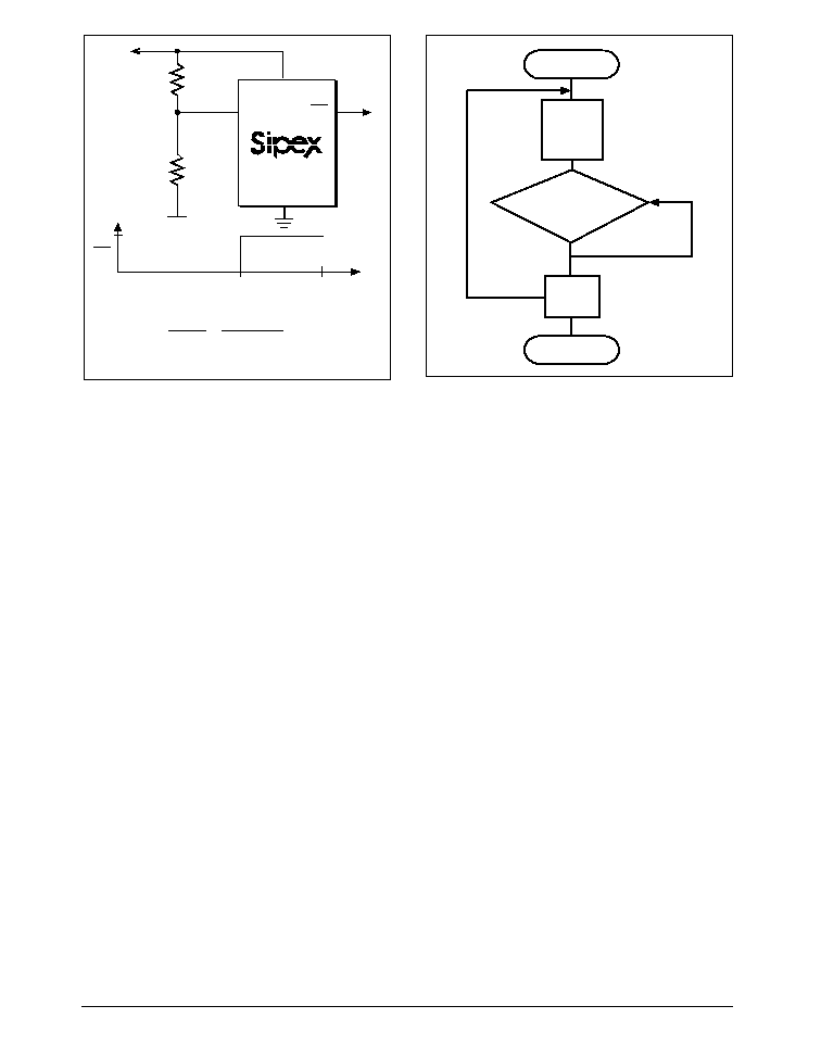
ADDING HYSTERESIS TO THE
POWER-FAIL COMPARATOR
Hysteresis adds a noise margin to the power-fail
comparator and prevents repeated triggering of
PFO when VIN is near the trip point. Figure 14
shows how to add hysteresis to the power-fail
comparator. Select the ratio of R1 to R2 such
that PFI sees 1.25V when VIN falls to the de-
sired trip point (VTRIP). Resistor R3 adds hys-
teresis. It will typically be an order of magni-
tude greater than R1 or R2. The current through
R1 and R2 should be at least 1
Ķ
A to ensure that
the 25nA (max) PFI input current does not shift
the trip point. R3 should be larger than 10k
to
prevent it from loading down the PFO pin. Ca-
pacitor C1 adds additional noise rejection.
MONITORING A NEGATIVE VOLTAGE
The power-fail comparator can be used to moni-
tor a negative supply voltage using the circuit
shown in Figure 15. When the negative supply
is valid, PFO is low. When the negative supply
voltage drops, PFO goes high. This circuit's ac-
curacy is affected by the PFI threshold tolerance,
the V
CC
voltage, and resistors R1 and R2.
BACKUP-BATTERY REPLACEMENT
The backup battery may be disconnected while
V
CC
is above the reset threshold. No precautions
are necessary to avoid spurious reset pulses.
Figure 14. Adding Hysteresis to the Power-Fail Comparator
Figure 13. Alternate CE Gating
Corporation
CE
IN
CE
OUT
V
OUT
GND
CE
CE
CE
CE
CE
CE
CE
CE
Rp
*
*
MAXIMUM Rp VALUE DEPENDS ON
THE NUMBER OF RAM DEVICES.
MINIMUM Rp VALUE IS 1K
ACTIVE-HIGH CE
LINES FROM LOGIC
RAM 1
RAM 2
RAM 3
RAM 4
VIN
R1
R2
R3
C1*
+5V
PFI
PFO
GND
TO
Ķ
P
+5V
PFO
OV
OV
* OPTIONAL FOR ADDITIONAL
NOISE REJECTION
V
L
V
TRIP
V
H
R1 + R2
R2
(
)
R2 II R3
R1 + R2 II R3
(
)
V
L
- 1.25 5 - 1.25 1.25
R1 R3 R2
Corporation
Vcc
V
H
= 1.25
V
TRIP
= 1.25 *
V
IN
+
=
SP791DS/08 SP791 Low Power Microprocessor Supervisory with Battery Switch-Over
© Copyright 2000 Sipex Corporation
16
Figure 16. Watchdog Flow Diagram
Figure 15. Monitoring a Negative Voltage
NEGATIVE-GOING V
CC
TRANSIENTS
The SP791 is relatively immune to short-dura-
tion negative-going V
CC
transients resulting
from power up, power down, and brownout con-
ditions. It is usually undesirable to reset the
Ķ
P
when V
CC
experiences only small glitches.
Typically, a V
CC
transient that goes 100mV be-
low the reset threshold and lasts for 40
Ķ
s or less
will not cause a reset pulse to be issued.
A 100nF bypass capacitor mounted close to the
V
CC
pin provides additional transient immunity.
CONNECTING A TIMING CAPACITOR
TO THE SWT PIN
To prevent timing errors minimize external cur-
rent leakage sources at this pin, and locate the
capacitor as close to SWT as possible. The sum
of PC board leakage + SWT capacitor leakage
must be small compared to
Ī
100 nA.
WATCHDOG SOFTWARE
CONSIDERATIONS
A way to help the watchdog timer keep a closer
watch on software execution involves setting
and resetting the watchdog input at different
points in the program, rather than "pulsing" the
watchdog input high-low-high or low-high-low.
This technique avoids a "stuck" loop where the
watchdog timer continues to be reset within the
loop, keeping the watchdog from timing out.
Figure 16 shows an example flow diagram
where the I/O driving the watchdog input is set
low at the beginning of the program, set high at
the beginning of every subroutine or loop, then
set low again when the program returns to the
beginning. If the program should "hang" in any
subroutine, the I/O is continually set high and
the watchdog timer is allowed to time out, caus-
ing a reset or interrupt to be issued.
MAXIMUM VCC FALL TIME
The V
CC
fall time is limited by the propagation
delay of the battery switchover comparator and
should not exceed 0.03V/
Ķ
s. A standard rule of
thumb for filter capacitance on most regulators
is on the order of 100
Ķ
F per amp of current.
When the power supply is shut off or the main
battery is disconnected, the associated initial
V
CC
fall rate is just the inverse of 1A/100
Ķ
F =
0.01V/
Ķ
s. The V
CC
fall rate decreases with time
as V
CC
falls exponentially, which more than sat-
isfies the maximum fall-time requirement.
+5V
R1
R2
V≠
PFO
+5V
0V
V
TRIP
0V
GND
PFI
Vcc
PFO
5 - 1.25 1.25 - V
TRIP
R1 R2
=
NOTE: V
TRIP
IS NEGATIVE.
Corporation
V≠
START
SET
WDI
LOW
SUBROUTINE
OR PROGRAM LOOP
SET WDI
HIGH
RETURN
END
17
SP791DS/08 SP791 Low Power Microprocessor Supervisory with Battery Switch-Over
© Copyright 2000 Sipex Corporation
D
ALTERNATE
END PINS
(BOTH ENDS)
D1 = 0.005" min.
(0.127 min.)
E
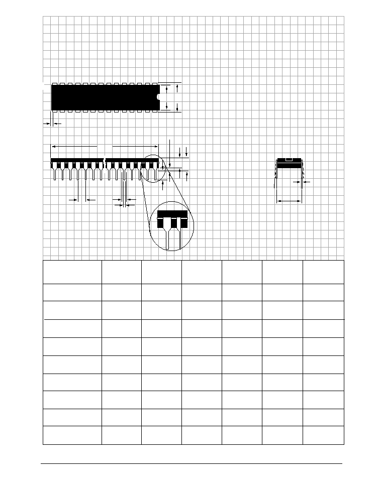
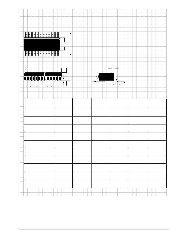
PACKAGE: PLASTIC
DUAL≠IN≠LINE
(NARROW)
DIMENSIONS (Inches)
Minimum/Maximum
(mm)
A = 0.210" max.
(5.334 max).
E1
C
ō
L
A2
A1 = 0.015" min.
(0.381min.)
B
B1
e = 0.100 BSC
(2.540 BSC)
e
A
= 0.300 BSC
(7.620 BSC)
A2
B
B1
C
D
E
E1
L
ō
0.115/0.195
(2.921/4.953)
0.014/0.022
(0.356/0.559)
0.045/0.070
(1.143/1.778)
0.008/0.014
(0.203/0.356)
0.735/0.775
(18.669/19.685)
0.300/0.325
(7.620/8.255)
0.240/0.280
(6.096/7.112)
0.115/0.150
(2.921/3.810)
0į/ 15į
(0į/15į)
0.115/0.195
(2.921/4.953)
0.014/0.022
(0.356/0.559)
0.045/0.070
(1.143/1.778)
0.008/0.014
(0.203/0.356)
0.355/0.400
(9.017/10.160)
0.300/0.325
(7.620/8.255)
0.240/0.280
(6.096/7.112)
0.115/0.150
(2.921/3.810)
0į/ 15į
(0į/15į)
22≠PIN
8≠PIN
14≠PIN
16≠PIN
0.115/0.195
(2.921/4.953)
0.014/0.022
(0.356/0.559)
0.045/0.070
(1.143/1.778)
0.008/0.014
(0.203/0.356)
1.145/1.155
(29.083/29.337)
0.300/0.325
(7.620/8.255)
0.240/0.280
(6.096/7.112)
0.115/0.150
(2.921/3.810)
0į/ 15į
(0į/15į)
0.115/0.195
(2.921/4.953)
0.014/0.022
(0.356/0.559)
0.045/0.070
(1.143/1.778)
0.008/0.014
(0.203/0.356)
0.780/0.800
(19.812/20.320)
0.300/0.325
(7.620/8.255)
0.240/0.280
(6.096/7.112)
0.115/0.150
(2.921/3.810)
0į/ 15į
(0į/15į)
18≠PIN
0.115/0.195
(2.921/4.953)
0.014/0.022
(0.356/0.559)
0.045/0.070
(1.143/1.778)
0.008/0.014
(0.203/0.356)
0.880/0.920
(22.352/23.368)
0.300/0.325
(7.620/8.255)
0.240/0.280
(6.096/7.112)
0.115/0.150
(2.921/3.810)
0į/ 15į
(0į/15į)
20≠PIN
0.115/0.195
(2.921/4.953)
0.014/0.022
(0.356/0.559)
0.045/0.070
(1.143/1.778)
0.008/0.014
(0.203/0.356)
0.980/1.060
(24.892/26.924)
0.300/0.325
(7.620/8.255)
0.240/0.280
(6.096/7.112)
0.115/0.150
(2.921/3.810)
0į/ 15į
(0į/15į)
SP791DS/08 SP791 Low Power Microprocessor Supervisory with Battery Switch-Over
© Copyright 2000 Sipex Corporation
18
D
E
H
PACKAGE: PLASTIC
SMALL OUTLINE (SOIC)
(NARROW)
DIMENSIONS (Inches)
Minimum/Maximum
(mm)
8≠PIN
A
A1
ō
L
B
e
h x 45į
A
A1
B
D
E
e
H
h
L
ō
0.053/0.069
(1.346/1.748)
0.004/0.010
(0.102/0.249
0.014/0.019
(0.35/0.49)
0.189/0.197
(4.80/5.00)
0.150/0.157
(3.802/3.988)
0.050 BSC
(1.270 BSC)
0.228/0.244
(5.801/6.198)
0.010/0.020
(0.254/0.498)
0.016/0.050
(0.406/1.270)
0į/8į
(0į/8į)
14≠PIN
0.053/0.069
(1.346/1.748)
0.004/0.010
(0.102/0.249)
0.013/0.020
(0.330/0.508)
0.337/0.344
(8.552/8.748)
0.150/0.157
(3.802/3.988)
0.050 BSC
(1.270 BSC)
0.228/0.244
(5.801/6.198)
0.010/0.020
(0.254/0.498)
0.016/0.050
(0.406/1.270)
0į/8į
(0į/8į)
16≠PIN
0.053/0.069
(1.346/1.748)
0.004/0.010
(0.102/0.249)
0.013/0.020
(0.330/0.508)
0.386/0.394
(9.802/10.000)
0.150/0.157
(3.802/3.988)
0.050 BSC
(1.270 BSC)
0.228/0.244
(5.801/6.198)
0.010/0.020
(0.254/0.498)
0.016/0.050
(0.406/1.270)
0į/8į
(0į/8į)
19
SP791DS/08 SP791 Low Power Microprocessor Supervisory with Battery Switch-Over
© Copyright 2000 Sipex Corporation
ORDERING INFORMATION
Model
Temperature Range
Package
SP791CP ................................................................................... 0įC to +70įC .............................................................................. 16-pin, Plastic DIP
SP791CN ................................................................................... 0įC to +70įC .......................................................................... 16-pin, Narrow SOIC
SP791EP .................................................................................... -40įC to +85įC .......................................................................... 16≠pin, Plastic Dip
SP791EN ................................................................................... -40įC to +85įC ..................................................................... 16≠pin, Narrow SOIC
Sipex Corporation reserves the right to make changes to any products described herein. Sipex does not assume any liability arising out of the
application or use of any product or circuit described hereing; neither does it convey any license under its patent rights nor the rights of others.
Corporation
SIGNAL PROCESSING EXCELLENCE
Please consult the factory for pricing and availability on a Tape-On-Reel option.
Sipex Corporation
Headquarters and
Sales Office
22 Linnell Circle
Billerica, MA 01821
TEL: (978) 667-8700
FAX: (978) 670-9001
e-mail: sales@sipex.com
Sales Office
233 South Hillview Drive
Milpitas, CA 95035
TEL: (408) 934-7500
FAX: (408) 935-7600