 | –≠–ª–µ–∫—Ç—Ä–æ–Ω–Ω—ã–π –∫–æ–º–ø–æ–Ω–µ–Ω—Ç: SP791EB | –°–∫–∞—á–∞—Ç—å:  PDF PDF  ZIP ZIP |
1
SP791 Evaluation Board Manual
SP791EB/04
©Copyright 2000 Sipex Corporation
SP791
Evaluation Board
Manual
s
Easy Evaluation for the
SP791 Microprocessor
Supervisory Circuit
s
Probe Points Accessible
for all SP791 Pins
s
16 Pin Narrow SOIC or
DIP Sockets Available
for the SP791 Circuit
s
Convenient Layout of
Input Option Probe
Points
DESCRIPTION...
The SP791 Evaluation Board is designed to help analyze the many functions of the SP791
µ
P Supervisory circuit. The evaluation board provides easy probe access points to all SP791
pins so that the user can measure electrical characteristics and waveforms of each signal.
The SP791 Evaluation Board also provides solder pads for DIP or SOIC packages, as well
as options for DIP or SOIC sockets for easy evaluation of multiple devices.
The next two sections describe the SP791 Board Layout and Using the SP791 Evaluation
Boards. A table of SP791 Pin Assignments is also included with a section on Power Supply
Connections. A SP791 Evaluation Board List of Materials is provided with some
manufacturers part numbers to use as a reference. Finally, a schematic is included of the
SP791 Evaluation Board.
Æ

2
SP791 Evaluation Board Manual
SP791EB/04
©Copyright 2000 Sipex Corporation
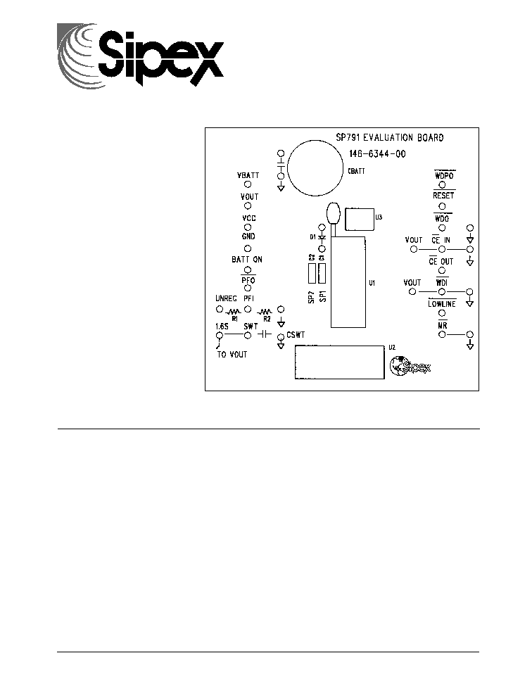
BOARD LAYOUT
The SP791 Evaluation Board has been
designed to easily and conveniently provide
access to all pins of the SP791 device under test.
Position the board with the silkscreen lettering
upright (also see drawing on the front page of
this manual) and you will see two vertical rows
of eight pins each, which represent the 16 pins of
the SP791 device starting in the top left with
V
BATT
as pin one. The pin receptacles are raised
female pins which can accommodate easy-
hook connection leads for power and meter
connections, as well as scope probe hooks and
grounds for waveform measurements.
The 16 pin SP791 may be installed in one of 3
locations: U1 for DIP or DIP sockets, U3 for
SOICs or U2 for SOIC sockets. The five input
pins for the SP791 are provided with extra Input
Probe Points for connecting inputs to these pins.
For example pin 11 WDI has nearby pins V
OUT
and GND to connect to for evaluation of WDI
timeout. These female receptacle pins can be
jumpered together with easy-hook connectors
or stripped back solid wire leads. In the case of
inputs SWT or PFI, a resistor or capacitor with
leads may be pushed into the female receptacle
pins to make easy connections. Also, mating
male pins (see List of Materials) may be
soldered to the components and inserted into the
receptacle pins.
USING THE EVALUATION BOARD
Connect the SP791 Evaluation Board to the
power supplies for V
CC
and V
BATT
(see the
section Power Supply Connections following
the table SP791 Pin Assignments). It is good
practice to not switch power on until power
connections are made to the evaluation board.
Evaluating Pin Functions
Pin 1 - V
BATT
- Backup-Battery Input.
Connect to external supply, battery or capacitor
and charging circuit.
Pin 2 - V
OUT
- Output Supply Voltage. This
function is used to provide power supply
switching of either V
CC
or V
BATT
to an
external device like a CMOS RAM to ensure a
constant supply for the memory. To evaluate
this function, vary the V
CC
voltage for a set
V
BATT
voltage until you simulate the following
conditions: V
OUT
connects to V
CC
when V
CC
is greater than V
BATT
and V
CC
is above the reset
threshold. When V
CC
falls below V
BATT
and
V
CC
is below the reset threshold, V
OUT
connects
to V
BATT
. Start with V
BATT
voltage of about 2.8
to 4.0 V and vary V
CC
from 0V to 5V to 0V and
observe V
OUT
. (Note: a 0.1
µ
F bypass capacitor
(C1) is connected from V
OUT
to GND).
Pin 3 - V
CC
- Input Supply Voltage - +5V input.
A 0.1
µ
F bypass capacitor (C2) is connected
from V
CC
to GND.
Pin 4 - GND - Ground reference for all signals.
Pin - 5 - BATT ON - Battery On Output.
Goes high when V
OUT
switches to V
BATT
. Goes
low when V
OUT
switches to V
CC
. Connect the
base of a PNP through a current-limiting resistor
to BATT ON for V
OUT
current requirements
greater than 250mA.
Pin 6 - PFO - Power-Fail Output. This is the
output of the power-fail comparator. PFO, goes
low when PFI is less than1.25V. This is an
uncommitted comparator, and has no effect on
any other internal circuitry.
Pin 7 - PFI - Power-Fail Input. This is the
non-inverting input to the power-fail comparator.
When PFI is less than 1.25V, PFO goes low.
Connect PFI to GND or V
OUT
when not used.
Connect external divider R1 & R2 to Probe Pins
and connect Unregulated Voltage to UNREG
for Power Fail monitoring.
Pin 8 - SWT - Set Watchdog-Timeout Input.
Connect this input to V
OUT
to select the default
1.6 sec watchdog timeout period. Connect a
capacitor (C
SWT
) between the Probe Input Pins
SWT and GND to select another watchdog-
timeout period. Watchdog-timeout period = 2.1
x (capacitor value in nF) ms.
Pin 9 - MR - Manual-Reset Input. This input can
be tied to an external momentary pushbutton
switch, or to a logic gate output. RESET remains
low as long as MR is held Low and for 200ms
after MR returns high. Connect MR to Probe
Pin GND to cause a RESET active low.

3
SP791 Evaluation Board Manual
SP791EB/04
©Copyright 2000 Sipex Corporation
Pin 10 - LOWLINE - LOWLINE Output goes
low when V
CC
falls to 150mV above the reset
threshold. The output can be used to generate
a NMI (non-maskable interrupt) if the
unregulated supply is inaccessible
Pin 11 - WDI - Watchdog Input. WDI is a three-
level input. If WDI remains either high or low
for longer than the watchdog timeout period,
WDO goes low. WDO remains low until the
next transition at WDI. Leaving WDI
unconnected disables the watchdog function.
WDI connects to an internal voltage divider
between V
OUT
and GND, which sets it to
1.8V when left unconnected. For a simple check
of watchdog function, connect WDI to either
Probe pins GND or V
OUT
to cause WDO to go to
a Logic Low and produce pulses at WDPO
every 1.6 seconds. (typically 1.6 seconds unless
an external capacitor is used at the SWT pin).
Pin 12 - CE OUT - Chip-Enable Output. The
Chip-Enable (CE) function CE OUT provides
internal gating of chip enable signals to prevent
erroneous data from corrupting the CMOS RAM
in the event of a power failure. During normal
operation, the CE gate is enabled and all CE
transitions are passed from CE IN to CE OUT.
When Reset is asserted, this path is disabled.
Note that CE OUT goes low (active) only when
CE IN is low and V
CC
is above the reset thresh-
old. If CE IN is low when reset is asserted, CE
OUT will stay low for 15us or until CE IN goes
high, whichever occurs first.
Pin 13 - CE IN - Chip-Enable Input. The Input
to chip-enable gating circuit. Connect to GND
or V
OUT
if not used.
Pin 14 - WDO - Watchdog Output. WDO goes
low if WDI remains either high or low longer
than the watchdog timeout period. WDO returns
high on the next transition at WDI. WDO
remains high if WDI is unconnected. WDO is
also high when RESET is asserted.
Pin 15 - RESET - RESET Output goes low
whenever V
CC
falls below the reset threshold.
RESET will remain low for 200ms after V
CC
crosses the reset threshold on power-up.
Pin 16 - WDPO - Watchdog-Pulse Output.
Upon the absence of a transition at WDI,WDPO
will pulse low for 1ms. WDPO precedes WDO
by 70ns.
Note: To accurately measure the extremely small
supply current in Battery Back-up mode, you
need to cut split pads SP1 & SP2 (solder side of
board) severing connections to C1 & C2 which
would have leakage currents in the measurement
range. Also, remove charging circuit components
C
BATT
and D1 if they are installed.
4
SP791 Evaluation Board Manual
SP791EB/04
©Copyright 2000 Sipex Corporation
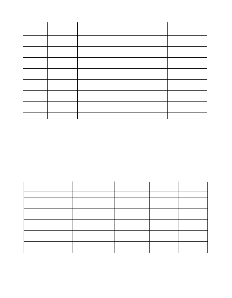
SP791 Pin Assignments
Pin No.
Pin Name
Pin Function
ActiveLevel
Input Pin Points
1
V
BATT
Backup-Battery Input
NA
2
V
OUT
Output Supply Voltage
NA
3
V
CC
Input Supply Voltage
NA
4
GND
Ground for all Signals
NA
5
BATT ON
Battery On Output
HIGH
6
PFO
Power-Fail Output
LOW
7
PFI
Power-Fail Input
HIGH
R1 & R2
8
SWT
Set Watchdog-Timeout Input
NA
1.6S or C
SWT
9
MR
Manual-Reset Input
LOW
GND
10
LOWLINE
Lowline Output
LOW
11
WDI
Watchdog Input
Transitions
V
OUT
& GND
12
CE OUT
Chip-Enable Output
LOW
13
CE IN
Chip-Enable Input
LOW
V
OUT
& GND
14
WDO
Watchdog Output
LOW
15
RESET
Reset Output
LOW
16
WDPO
Watchdog-Pulse Output
LOW
SP791 Pin Assignments
Power Supply Connections
Pin 3 -- V
CC
-- connect to external +5
VDC supply.
Pin 1 -- V
BATT
-- connect to external V+
supply of 2.8 to 4.0 VDC, or install capacitor
C
BATT
and charging diode D1 (see List of
Materials).
Pin 4 -- GND -- connect to negative or
ground of +5VDC supply and ground of V+
supply for V
BATT
Note: Ensure V
CC
, V
BATT
and GND
connections are made before operating device.
Part Number
Manufacturer
Ref. Des.
Quantity
uP Supervisor IC
SP791
Sipex
U3
1
Pin Receptacle-Female
300-1150-1472-7040
Mill-Max Mfg.
26
Ceramic Capacitor 0.1uF
Generic
C1, 2
2
Al. Spacers - 0.5"
8414
Keystone Elec.
4
6-32 Hex Nut
Generic
4
Optional:
16 Pin DIP Socket
216-3340-00-0602
3M - Textool
U1
1
16 Pin SOIC Socket
216-7383-55-1902
3M - Textool
U2
1
Maxcap 1F 5.5V
LC055105A
Cesiwid Inc.
C
BATT
1
Signal Diode
Generic
D1
1
Pin Receptacle - Male
3137-3002-10-0080
Mill-Max Mfg.
26
SP791 Evaluation Board List of Materials
Component
5
SP791 Evaluation Board Manual
SP791EB/04
©Copyright 2000 Sipex Corporation
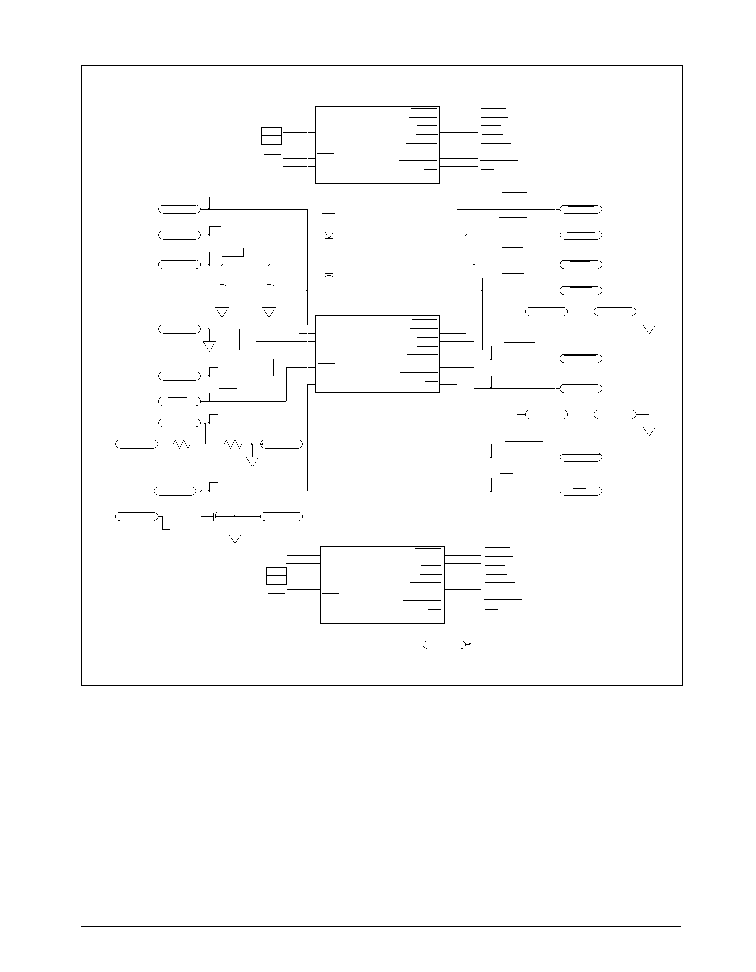
SP791 Evaluation Board Schematic
U3 -- SOIC
1
2
3
4
5
6
7
8
16
15
14
13
12
11
10
9
VBATT
VOUT
VCC
GND
BATT_ON
PFO
PFI
SWT
WDPO
RESET
WDO
CE IN
CE OUT
WDI
LOWLINE
MR
VBATT
VOUT
VCC
GND
BATT_ON
PFO
PFI
SWT
WDPO
RESET
WDO
CE IN
CE OUT
WDI
LOWLINE
MR
VBATT
VBATT
VOUT
VOUT
VCC
VCC
C2
C1
VCC
D1
(opt.)
Cbatt
(opt.)
GND
BATT_ON
BATTON
PFO
PFO
PFI
PFI
UNREG
R1
(opt.)
R2
(opt.)
R2
SWT
SWT
1.6S
VOUT
CSWT
Cswt (opt.)
WDPO
WDPO
RESET
RESET
WDO
WDO
CE IN
CE IN
VOUT
VOUT
GND
CE OUT
CE OUT
WDI
WDI
VOUT
VOUT
GND
LOWLINE
LOWLINE
MR
MR
VBATT
VOUT
VCC
GND
BATT_ON
PFO
PFI
SWT
WDPO
RESET
WDO
CE IN
CE OUT
WDI
LOWLINE
MR
16
15
14
13
12
11
10
9
1
2
3
4
5
6
7
8
SP791
SP791
U1 -- DIP
1
2
3
4
5
6
7
8
VBATT
VOUT
VCC
GND
BATT_ON
PFO
PFI
SWT
VBATT
VOUT
VCC
GND
BATT_ON
PFO
PFI
SWT
SP791
U2 -- SOIC SOCKET
16
15
14
13
12
11
10
9
WDPO
RESET
WDO
CE IN
CE OUT
WDI
LOWLINE
MR
WDPO
RESET
WDO
CE IN
CE OUT
WDI
LOWLINE
MR
VCC
NOTE: Probe Access Points as shown:
are for external connections by the user.
6
SP791 Evaluation Board Manual
SP791EB/04
©Copyright 2000 Sipex Corporation
ORDERING INFORMATION
Model .............................................................................................................................................................................................................. Package
SP791EB .............................................................................................................................................................................. SP791 Evaluation Board
SP791EK .................................................................................................................................................................................... SP791 Evaluation Kit
Corporation
SIGNAL PROCESSING EXCELLENCE
Sipex Corporation reserves the right to make changes to any products described herein. Sipex does not assume any liability arising out of the
application or use of any product or circuit described hereing; neither does it convey any license under its patent rights nor the rights of others.
Sipex Corporation
Headquarters and
Sales Office
22 Linnell Circle
Billerica, MA 01821
TEL: (978) 667-8700
FAX: (978) 670-9001
e-mail: sales@sipex.com
Sales Office
233 South Hillview Drive
Milpitas, CA 95035
TEL: (408) 934-7500
FAX: (408) 935-7600