 | –≠–ª–µ–∫—Ç—Ä–æ–Ω–Ω—ã–π –∫–æ–º–ø–æ–Ω–µ–Ω—Ç: SP8026 | –°–∫–∞—á–∞—Ç—å:  PDF PDF  ZIP ZIP |
1
Rev. 6/02/03
SP8024, 25, 26 200V/
µ
s Integrated APC Amplifier
© Copyright 2003 Sipex Corporation
200V/
µ
s Integrated APC Amplifier
with Gain Adjust & Differential Output
SP8024/8025/8026
Slew Rate of 200V/
µ
s
Fast Settling Time - 10ns
Gain Switch
2V Output Swing
Low Offset Voltage: < 10mV
Low Offset Drift: < 20
µ
V/
∞
C
12dB External Gain Adjust Range
Æ
DESCRIPTION
The SP8024, SP8025, and SP8026 are high-speed, differential output APC amplifiers that
integrate the photodiode and adjustable gain block on one chip. This allows the user to control
the laser power of the system in high-speed DVDRW, DVDRAM and CDRW systems. The wide
2V output swing also allows better system performance.
1
2
8
7
6
5
3
4
GAIN
GND
V
CC
V
OUT
+
SP8024/25/26
8 Pin COB
V
OUT
-
R
COM
R
GAIN1
R
GAIN2
GAIN
V
CC
GND
V
OUT
+
V
OUT
-
R
GAIN1
R
GCOM
TIA
R
G1
R
GAIN2
R
G2
Buffer
Buffer
1V
P-P
1V
P-P
50pF
1k
50pF
1k
(Flexible Flat Cable)
850
Rf1
Rf2
850
31
31
2463
2463
Advanced
FEATURES
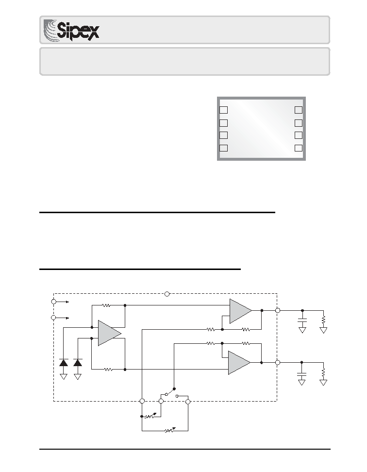
FUNCTIONAL DIAGRAM
2
Rev. 6/02/03
SP8024, 25, 26 200V/
µ
s Integrated APC Amplifier
© Copyright 2003 Sipex Corporation
These are stress ratings only and functional operation
of the device at these ratings or any other above those
indicated in the operation sections of the specifications
below is not implied. Exposure to absolute maximum
rating conditions for extended periods of time may
affect reliability.
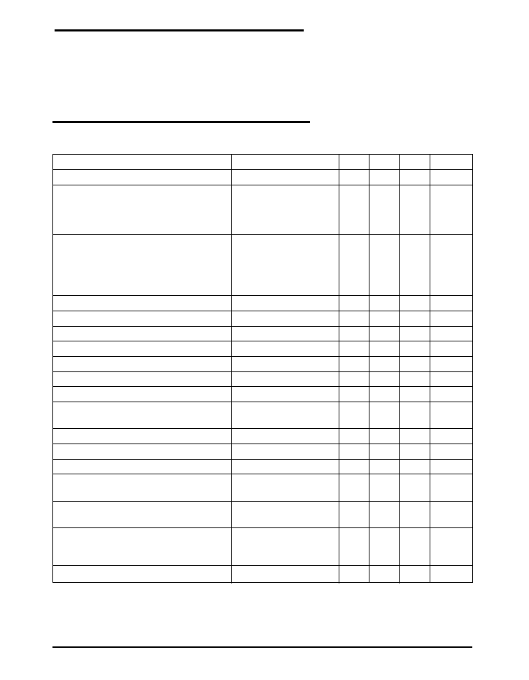
ELECTRICAL SPECIFICATIONS
Unless otherwise noted: V
CC
= +5.0V, C
LOAD
= 50pF to GND, R
GAIN
=262
and R
LOAD
= 1k
. -20
∞
C
T
A
+85
∞
C,
nominal gain
PARAMETER
CONDITIONS
MIN
TYP
MAX UNITS
Supply Voltage
4.5
5
5.5
V
Nominal Output Sensitivity
Any Select Mode
SP8024
ODB Gain
1000
V/W
SP8025
2000
SP8026
3000
Input Optical Power Required
Any Select Mode
to Produce 2 V Output Swing
ODB Gain
SP8024
2
mW
SP8025
1
SP8026
0.666
Full Scale Output Voltage Swing(Vp-p)
1.9
2
V
Output Common Mode Voltage
V
CC
/2
V
Differential Output Offset Voltage
-10
10
mV
Differential Output Offset Voltage Drift
-20
20
µ
V/
∞
C
Differential Output Noise
BW: 1kHz to 1MHz
1
2
mV
Differential Output Noise
BW: 1kHz to 100MHz
3
5
mV
Differential Output Slew Rate
200
250
V/
µ
s
Differential Output Settling Time
10
15
ns
to 1% of Final Value, 2V Step
Output Overshoot, 2V step
5
%
Bandwidth (-3db)
65
100
MHz
PSRR
4.5V < V
CC
< 5.5V
60
65
dB
Power Supply Current
T
A
= 25
∞
C
20
mA
Full Temp No Load
25
Gain Adjust Range
< 5% Overshoot,
-9
3
dB
150 < R
GAIN
< 1350
Input Voltage
Vlow(TTL Level)
0.8
V
Vhigh(TTL Level)
2.2
V
T
JA
, 3mm x 3.5mm Package
75
∞
C/W
T
J(MAX) ........................................................................................
120
∞
C
V
S(MAX) ...............................................................................................
6V
V
IN(MAX) ..............................................................................................
6V
ABSOLUTE MAXIMUM RATINGS
3
Rev. 6/02/03
SP8024, 25, 26 200V/
µ
s Integrated APC Amplifier
© Copyright 2003 Sipex Corporation
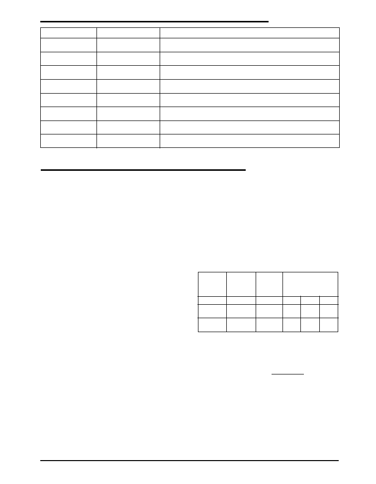
PIN DESCRIPTION
PIN NUMBER
NAME
FUNCTION
1
V
CC
Supply Voltage
2
GAIN
Gain Select
3
R
COM
Common connection point for R
GAIN
1 and R
GAIN
2
4
GND
Power Ground
5
R
GAIN1
Gain Adjust 1
6
R
GAIN2
Gain Adjust 2
7
V
OUT
-
Output Voltage -
8
V
OUT
+
Output Voltage +
Internal Operation
The SP8024/25/26 APC circuits have an inte-
grated photo detector and are designed with
three nominal sensitivities of 1mV/
µW, 2mV/
µW and 3mV/µW respectively. Each part's sen-
sitivity can also be adjusted continuously and
independently for two different gain modes via
two external resistors over a range of 12dB. The
two gain modes are controlled by a TTL com-
patible logic input. This logic input also normal-
izes the internal photo detector's responsivity
for 650nm and 780nm laser wavelengths. The
logic pin selects between the two external gain
setting resistors to allow independent control
and settings for the two gain functions.
The 8024 APC family uses two stages of gain to
optimize for speed and offset. The two stages
consist of a differential trans-impedance ampli-
fier (TIA), and a differential gain adjust ampli-
fier.
TIA
The first stage is a differential trans-impedance
amplifier (TIA) for converting the photo detec-
tor output current to a balanced differential
voltage. This topology allows for fast settling of
the photo detector and also cancels offset ef-
fects. The TIA has no external components.
Variable Gain Amplifier
This stage is used to vary the gain of the system.
It provides selection for two different gain set-
ting resistors, R
GAIN1
and R
GAIN2
, at pins 5 and
6 via internal MOSFET switches S1 and S2. The
logic input at pin 2 controls the selection of the
two external gain set resistors.
Table 1: Gain Select Logic Truth Table
Gain
Sensitivity
Select
Rexternal,
Gain
(mV/µW)
Pin 2
Pin 3 to:
Factor (x)
R
G1
= R
G2
= 262
SP8024
SP8025
SP8026
0 or Open
R
G1
- Pin 5
6.25
1
2
3
1
R
G2
- Pin 6
6.25
1
2
3
The gain of this balanced amplifier topology is
given by:
GAIN = 1 +
Rf1 + Rf2
R
EXT
where R
GAIN
is external and Rf1 = Rf2 = 850
in feedback.
The nominal gain is defined as 6.25.
THEORY OF OPERATION
4
Rev. 6/02/03
SP8024, 25, 26 200V/
µ
s Integrated APC Amplifier
© Copyright 2003 Sipex Corporation
There are internal buffering resistors and a
MOSFET switch resistance in series with the
external Rgain. These internal resistances add
up to a nominal value of 62
. Therefore the true
gain equation is:
GAIN = 1 +
Rf1 + Rf2
R
EXT
+ 62
This gives a nominal external Rgain value of
324 - 62 = 262
for a gain of 6.25.
The constraints on this stage are the parasitic
capacitances associated with the input pins. The
resistors used for setting the system gain are
actually subminiature potentiometers. They are
used for calibrating out systematic variations in
the optical path.
Pins 5 and 6 connect to the summing node of the
gain stage through MOSFET switches. When a
capacitor is added to the summing node of an
inverting amplifier it creates a pole in the re-
sponse. If this pole increases enough to interfere
with the internal compensation of the amplifier,
instability occurs. This instability appears as over-
shoot in the transient response. The stray capaci-
tance at pins 5 and 6 should be kept below 1pF.
This stage also allows the part to drive high
capacitive loads. The maximum load capaci-
tance is 50pF bulk. The actual load is typically
a flexible ribbon cable (FLEX) that acts like a
transmission line. This presents a distributed
capacitive load plus inductance and resistance.
In this case care should be taken to match the
characteristic impedance of the line at the far
end to avoid standing waves and ringing. The
buffer is designed to drive 1k
to ground. How-
ever, this resistor can be adjusted in value to
accommodate the characteristic impedance of
the signal trace.
Variable Gain Amplifier: continued
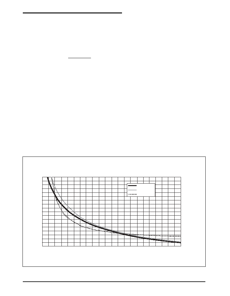
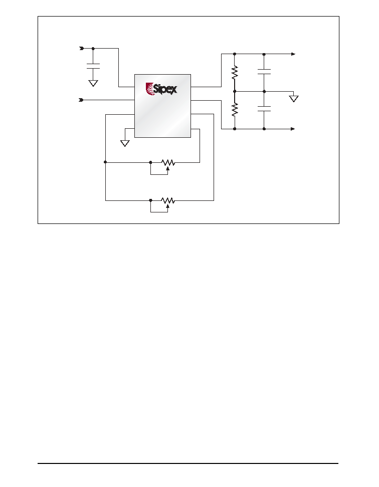
Figure 1. System Gain versus Gain Set Resisitor
SP8026 Differential APC Sensitivity
versus Gain Set Resistor
6.0
5.0
4.0
3.0
2.0
1.0
0.0
-1.0
-2.0
-3.0
-4.0
-5.0
-6.0
-7.0
-8.0
-9.0
-10.0
-11.0
-12.0
0
200
400
600
800
1000
1200
1400
1600
1800
2000
2200
Resistance ()
Gain (dB)
6.0
5.7
5.3
5.0
4.7
4.3
4.0
3.7
3.3
3.0
2.7
2.3
2.0
1.7
1.3
1.0
0.7
0.3
0.0
System Sensitivity (mV/
µ
W)
R
GAIN
R
EXT
Sensitivity
THEORY OF OPERATION : Continued
5
Rev. 6/02/03
SP8024, 25, 26 200V/
µ
s Integrated APC Amplifier
© Copyright 2003 Sipex Corporation
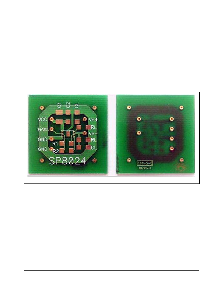
Layout and Routing Considerations
Special care must be taken when designing the
Flex or PCB for this part. The output peak
current requirement is in the order of 12.5mA
when driving 50pF of capacitive load with a
slew rate of 200V/s Therefore care must be
taken to provide low inductance, low resistance
paths for power and ground and output traces.
Supply coupling is also very important. Good
supply decoupling is important to ensure the
high frequency performance of the system by
eliminating supply lead inductance effects. The
decoupling capacitor C1 should be as close to
the part as possible. This capacitor should be
0.1
µF ceramic. C2 is optional to improve
decoupling and is recommended to be 1
µF tan-
Figure 2. Test and Evaluation PCB Layout for COB 8 Lead Package
Top
Bottom
talum. The layout of the PCB is pictured here.
Note the wide and short traces on the supply
lines.
The traces for the gain resistors R1 and R2 are
kept as short as possible to avoid excessive
parasitics. Any parasitics on these nodes will
limit the performance of the system. R1 and R2
are subminiature potentiometers in the applica-
tion. This is a single layer board done on FR4
material.
In order to minimize coupling capacitance into
the gain setting resistor nodes, it is also critical
that V
OUT
+ and V
OUT
- are routed away from the
traces associated with the gain-setting resistors.
6
Rev. 6/02/03
SP8024, 25, 26 200V/
µ
s Integrated APC Amplifier
© Copyright 2003 Sipex Corporation
Figure 3. Test and Evaluation Schematic
SP8024
SP8025
SP8026
1
2
3
4
8
7
6
5
V
OUT+
V
OUT-
R
GAIN2
R
GAIN1
R
G1
262
R
G2
262
V
CC
GAIN
R
GCOM
GND
GAIN
+5V
+
C1
0.1µF
+
CL1
50pF
+
CL2
50pF
RL1
1k
RL2
1k
V
OUT-
V
OUT+

7
Rev. 6/02/03
SP8024, 25, 26 200V/
µ
s Integrated APC Amplifier
© Copyright 2003 Sipex Corporation
1
2
3
4
8
7
6
5
H
0.090
0.600
D
b
e
L
BOTTOM VIEW
TOP VIEW
SIDE VIEW
5
∞
(2X)
E
A
C
F
S
B
PIN
SIDE VIEW
DETECTOR SIZE
0.35mm
Detector Area
0.70mm
8 PIN COB
(3.5mm x 3.0mm)
DIMENSIONS in
mm
Minimum/Maximum
8≠PIN
COB
A
B
b
c
D
E
e
H
L
F
S
0.90/1.10
.127/.33
0.30/0.50
0.50 nom
2.90/3.10
3.00/3.20
0.75 nom
3.40/3.60
0.40/0.60
0.28/0.48
0.075/0.275
PACKAGE : 8 PIN COB
8
Rev. 6/02/03
SP8024, 25, 26 200V/
µ
s Integrated APC Amplifier
© Copyright 2003 Sipex Corporation
ORDERING INFORMATION
Part Number
Temperature Range
Package Type
SP8024 ................................................... -20
∞
C to +85
∞
C .............. 8 lead COB (3.0mm x 3.5mm)
SP8025 ................................................... -20
∞
C to +85
∞
C .............. 8 lead COB (3.0mm x 3.5mm)
SP8026 ................................................... -20
∞
C to +85
∞
C .............. 8 lead COB (3.0mm x 3.5mm)
ANALOG EXCELLENCE
Sipex Corporation reserves the right to make changes to any products described herein. Sipex does not assume any liability arising out of the
application or use of any product or circuit described herein; neither does it convey any license under its patent rights nor the rights of others.
Corporation
Sipex Corporation
Headquarters and
Sales Office
233 South Hillview Drive
Milpitas, CA 95035
TEL: (408) 934-7500
FAX: (408) 935-7600
Sales Office
22 Linnell Circle
Billerica, MA 01821
TEL: (978) 667-8700
FAX: (978) 670-9001
e-mail: sales@sipex.com