
Rev 0.8 (09/25/06) SP8036 APC Amplifier 2006 Sipex Corporation
page
1
of
6
1
2
3
4
8
7
6
5
Vref
Rgain1
Rgain2
CE
SP8036
8-Pin
OPLGA
Vcc
Gain
Vout
Gnd
__
FEATURES
�
Dual wavelength 650nm and 780nm
�
13 ns Settling Time to 2%
�
100 MHz Bandwidth at -3dB
�
10 mV Output Offset Voltage
�
25 �V/
o
C Output Offset Voltage Drift
�
� 6 dB External Gain Adjust
�
Small 8-pin OPLGA package
�
Power-down mode
APPLICATIONS
CD-R, and CD-RW
DVD+/-R, DVD+/-RW, and DVD-
RAM
GENERAL DESCRIPTION
The SP8036 represents the next generation in Automatic Power Control (APC) amplifiers designed
specifically for demanding pick-up head applications. With its integrated photo detector, the SP8036 monitors
light intensity of the laser diode in CD-R, CD-RW, DVD+/-R, DVD+/-RW, and DVD-RAM assemblies and
converts this light to an output voltage. The magnitude of this voltage signal corresponds to the laser power
intensity and is subsequently fed back to the laser diode driver to control the laser output power.
The SP8036 on-chip photo detector transforms incident laser light into a proportional current, which is then
converted to a voltage through a transimpedance amplifier. Adjustable gain is provided in the transimpedance
amplifier by means of a gain control loop that is controlled by an external resistor. This external resistor is not
a part of the signal path, which greatly reduces the effects of all parasitic capacitances and inductances on
the flex cable at these pins. The signal is then buffered to provide reactive load drive capability.
The SP8036 achieves an unparalleled level of performance by combining excellent DC stability and low noise
with outstanding AC performance. This level of performance is achieved using a proprietary fully
complimentary BICMOS process with fully integrated, on-board photo detector.
The SP8036 is offered with a nominal sensitivity 4450 V/W and is packaged in a 3.0 x 3.5 mm, 8-lead
OPLGA package. All input logic levels should not be left open at any time.
The SP8036 offers power-down capability with the new active-low chip enable pin, CE. The chip operates
normally when this pin is connected to GND and powers down when connected to Vcc.
Solved by
TM
SP8036
APC Amplifier with Integrated Photodiode
and Gain Adjust Capability

Rev 0.8 (09/25/06) SP8036 APC Amplifier 2006 Sipex Corporation
page
2
of
6
FUNCTIONAL DIAGRAM
Figure 1: Functional Diagram
ABSOLUTE MAXIMUM RATINGS
These are stress ratings only and functional operation of the device at these ratings or any other above those
indicated in the operation sections of the specifications below is not implied. Exposure to absolute maximum
rating conditions for extended periods of time may affect reliability.
Supply Voltage (Vcc)....................................6.0V
All Other Pins............. ............................... 6.0V
Junction Temperature (T
J
)...........................120
o
C
Storage Temperature....................-40�C to +100�C
Soldering Temperature.............................+235�C
RECOMMENDED OPERATING CONDITIONS
Supply Voltage (Vcc)..........................4.5V to 5.5V
Reference Voltage (V
REF
) ...................1.9V to 2.3V
Operating temperature......................-20 to +85
o
C
THERMAL SPECIFICATIONS
8-pin OPLGA (3 x 3.5mm) Package Thermal Resistance............90
o
C/W
Rev 0.8 (09/25/06) SP8036 APC Amplifier 2006 Sipex Corporation
page
3
of
6
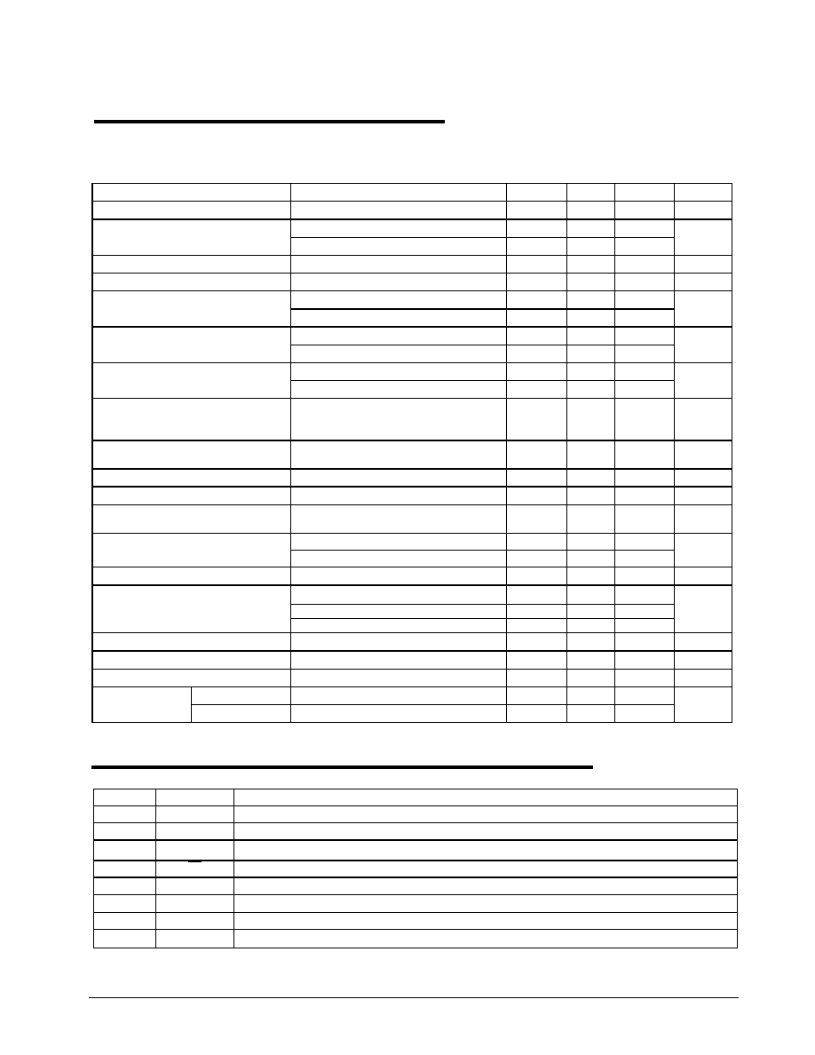
ELECTRICAL/OPTICAL SPECIFICATIONS
Unless otherwise noted: 4.5V Vcc 5.5V, V
REF
=2.1V, output load: R
L
= 1k to V
REF
, C
L
= 20pF to GND, R
GAIN
=
400ohm,
ambient temperature -20
o
C T
A
+85
o
C
Parameter
Conditions
Min
Typ
Max
Units
Supply Voltage
4.5
5
5.5
V
T
A
= 25
o
C, no signal
13
18
Supply Current
-20 T
A
+85
o
C, no signal
25
mA
Voltage Reference Range
R
GAIN
= 400ohm
1.9
2.1
2.3
V
Output Offset Voltage
Referenced to V
REF
-10
10
mV
R
GAIN
= 400ohm
-25
25
Output Offset Voltage Drift
R
GAIN
= 950ohm
-50
50
�
V/
o
C
R
GAIN
= 400ohm, 4.5V Vcc 5.5V
55
73
Power Supply Rejection Ratio
(PSRR) *
R
GAIN
= 950ohm, 4.5V Vcc 5.5V
50
75
dB
Logic level low
0.8
Gain Switch Logic Levels
Logic level high
2.4
V
Output Sensitivity
Any Select Mode.
Laser Beam Diameter = 0.70mm,
uniform density (R
GAIN
= 400ohm)
4450
V/W
Input Optical Power required to
produce a 1.5V output swing
Any Select Mode
R
GAIN
= 400ohm
0.34
mW
Photo Detector Active Area
0.25
mm
2
Output Sensitivity Change vs. Vcc
R
GAIN
= 950ohm
5
%/V
Output Sensitivity Change vs.
Temperature
R
GAIN
= 950ohm
0.1
%/
o
C
1kHz BW 1MHz
0.14
2
Output Noise (+6 dB)
1kHz BW 100MHz
1.28
5
mV
Output Slew Rate
190
V/�s
-6dB
12.6
15
0dB
13.1
15
Output Settling Time to 2% of
finale value (1.5V step)
+6dB
14.0
15
ns
Full Scale Output Voltage Swing
Referenced to V
REF
-1.5
-1.7
Vp-p
Output Overshoot
V
OUT
=1.5V step
5
%
Bandwidth (-3dB)
R
GAIN
= 400ohm
70
100
MHz
Vcc = 5.0V
150ohmR
GAIN
950ohm
-6
+6
Gain Adjust
Range at
Vcc = 4.5V
250ohmR
GAIN
950ohm
-3
+6
dB
* PSRR = 20log (Vcc/V
OUT
), where V
OUT
is the output voltage without signal (offset voltage)
PIN ASSIGNMENTS
Pin #
Pin Name
Pin Function
1
Vref
Reference Voltage
2
Rgain1
Gain Adjust Resistor R
GAIN
1
connection point
3
Rgain2
Gain Adjust Resistor R
GAIN
2
connection point
4
CE
Active low Chip enable
5
GND
Power Ground
6
Vout
Output Voltage
7
Gain
Gain Switch Input. Low level or Open selects pin R
GAIN
1
, high level selects pin R
GAIN
2
8
Vcc
Supply Voltage. Bypass to GND with ceramic capacitor 0.1�F

Rev 0.8 (09/25/06) SP8036 APC Amplifier 2006 Sipex Corporation
page
4
of
6
PHOTO DETECTOR PATTERN

Rev 0.8 (09/25/06) SP8036 APC Amplifier 2006 Sipex Corporation
page
5
of
6
OPLGA 8-pin PACKAGE DIMENSIONS

Rev 0.8 (09/25/06) SP8036 APC Amplifier 2006 Sipex Corporation
page
6
of
6
ORDERING INFORMATION
Part number
Temperature range
Package Type
SP8036DG4
-20 + 85
0
C
8-pin OPLGA