 | –≠–ª–µ–∫—Ç—Ä–æ–Ω–Ω—ã–π –∫–æ–º–ø–æ–Ω–µ–Ω—Ç: SP8059CE | –°–∫–∞—á–∞—Ç—å:  PDF PDF  ZIP ZIP |

ADVANCED
SP8059
Rev 0.7e (05-17-05) SP8059 Ten-Channel Photo detector IC Copyright 2005 Sipex Corporation
SIPEX RESERVES THE RIGHT TO MAKE CHANGES TO THIS DATASHEET. CALL FOR UPDATES: 1-408-934-7500.
SIPEX CONFIDENTIAL, PRELIMINARY & PROPRIETARY. DO NOT DISTRIBUTE OR
COPY
page
1
of
4
1
2
3
4
5
6
7
8
16
15
14
13
12
11
10
9
A
D
Vcc
RF+
RF-
GND
B
C
E
G
Vref
Gain 1
Gain 0
Gain 2
F
H
SP8059
16-Pin
OLCC
FEATURES
∑
Triple wavelength support: 405, 650 and 780nm
∑
72MHz Data channel bandwidth at -1dB linearity
∑
Selectable gain and Power Down Mode
∑
Available in wafer form or
5.0 x 4.0 mm 16-pin OLCC package
APPLICATION
∑
4X Blu-Ray Read/Write
∑
X16 DVD Read/Write
∑
X48 CD Read/Write
GENERAL DESCRIPTION
The SP8059 is a ten-channel photo detector IC (PDIC) designed for new generation of Blu-Ray
DVD and standard DVD/CD applications and can operate at wavelengths of 405, 650 and 780
nm. The device contains three photo diode (sensor) arrays, one of them with four identical
sensors A ≠ D and the other two with two sensors each (E, F and G, H respectively). The ten
channels consist of four high speed channels (A, B, C, and D), four slow channels (E, F, G, and
H), and two RF channel with paraphrase output (RF+ and RF-). The high speed channels output
a signal from one of the sensors A ≠ D. The E, F, G, and H channel outputs are used for servo
control. The RF channels output is the sum of A + B + C + D channels with identical weights
given to all channels.
Three Gain select inputs allow the setting of eight gain modes and a Power Down mode with low
power consumption if Gain 0 input is left floating.
Low noise operation enables data recovery at very low signal levels.
10 Channel Photo Detector IC

ADVANCED
SP8059
Rev 0.7e (05-17-05) SP8059 Ten-Channel Photo detector IC Copyright 2005 Sipex Corporation
SIPEX RESERVES THE RIGHT TO MAKE CHANGES TO THIS DATASHEET. CALL FOR UPDATES: 1-408-934-7500.
SIPEX CONFIDENTIAL, PRELIMINARY & PROPRIETARY. DO NOT DISTRIBUTE OR
COPY
page
2
of
4
PIN ASSIGNMENTS
Pin #
Pin Name
Pin Function
1
A
Output of A channel
2
D
Output of D channel
3
Vcc
Supply voltage. Bypass to GND with ceramic capacitor 0.1uF
4
RF+
Output of RF+ channel. RF+ = 0.375 (A + B + C + D)
5
RF-
Output of RF- channel. RF- = -0.375 (A + B + C + D)
6
GND
Ground pin
7
B
Output of B channel
8
C
Output of C channel
9
H
Output of H channel
10
F
Output of F channel
11
Gain 2
Gain switch input.
12
Gain 0
Gain switch input.
13
Gain 1
Gain switch input.
14
Vref
Reference voltage. Bypass to GND with ceramic capacitor 0.1uF
15
G
Output of G channel
16
E
Output of E channel
BOARD LAYOUT AND GROUNDING
To obtain the best performance from the SP8059, a printed circuit board with ground plane is
required. Ground pins (pin #6) should be connected to the ground plane. High quality, low series
resistance ceramic 0.1uF bypass capacitors should be used at the Vcc and Vref pins (pins #3 and
#14). These capacitors must be located as close to the pins as possible. The traces connecting
the pins to the ground plane, Vcc, Vref, and bypassing capacitors must be kept short and should
be made as wide as possible.
ADVANCED
SP8059
Rev 0.7e (05-17-05) SP8059 Ten-Channel Photo detector IC Copyright 2005 Sipex Corporation
SIPEX RESERVES THE RIGHT TO MAKE CHANGES TO THIS DATASHEET. CALL FOR UPDATES: 1-408-934-7500.
SIPEX CONFIDENTIAL, PRELIMINARY & PROPRIETARY. DO NOT DISTRIBUTE OR
COPY
page
3
of
4
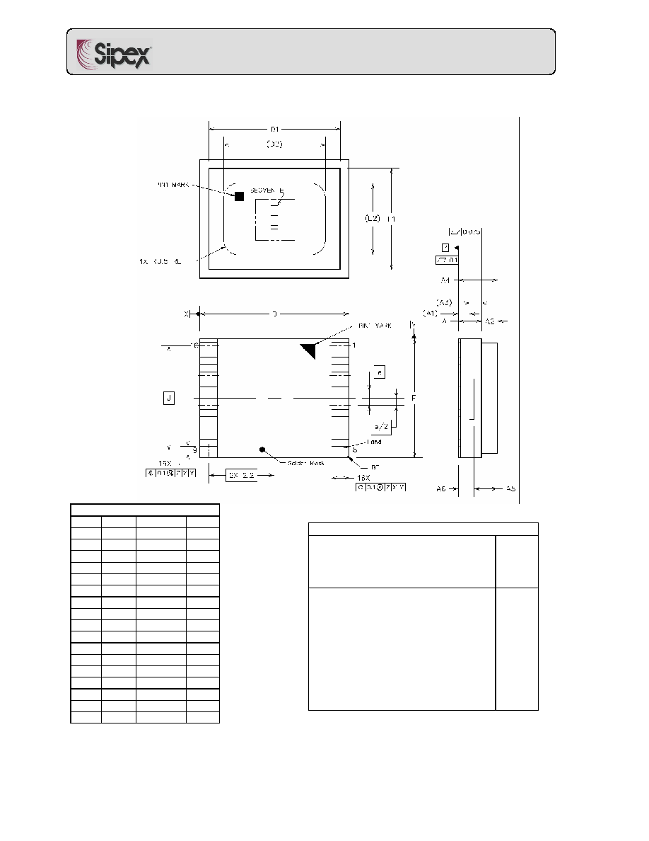
16-PIN ORGANIC LEADLESS CHIP CARRIER (OLCC) PACKAGE DIMENSIONS
Dimensions, millimeters
Dim.
Min.
Nom.
Max.
A
0.85
0.96
1.07
A1
0.36 ref
A2
0.25
0.30
0.35
A3
0.6 ref
A4
1.15
1.31
1.47
A5
0.54
0.68
0.82
A6
0.48
0.57
0.66
b
0.2
0.25
0.3
D
4.9
5.0
5.1
D1
4.3
4.4
4.5
D2
3.4 ref
E
3.9
4.0
4.1
E1
3.3
3.4
3.5
E2
2.4ref
e
0.5 BSC
L
0.5
0.6
0.7
J
3.5 BSC
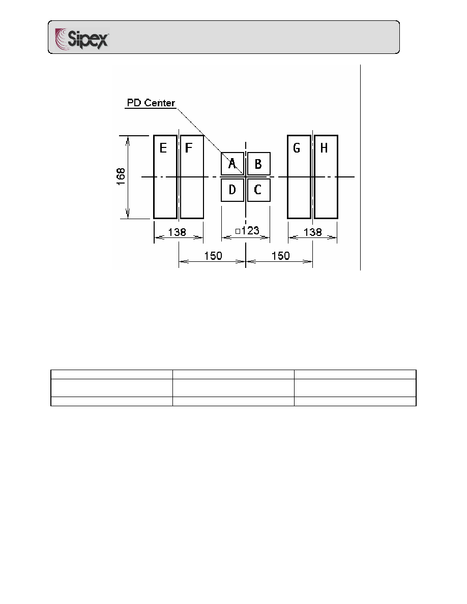
Location of the photo detectors in a package
X0 = 0 ± 50µm
Y0 = 0 ± 50µm
Z0 (A6) = 570 ± 90µm
= 0 ± 1.0
0
Optical center stability X, Y to
package soldering reference in any
radial direction at overall operational
temperature and life time .........
Optical center stability Z to package
soldering reference over operational
temperature range, including optical
window properties ...
Tilt to optical surface die with respect
to soldering reference ............
< TBD
< TBD
< 1%
ADVANCED
SP8059
Rev 0.7e (05-17-05) SP8059 Ten-Channel Photo detector IC Copyright 2005 Sipex Corporation
SIPEX RESERVES THE RIGHT TO MAKE CHANGES TO THIS DATASHEET. CALL FOR UPDATES: 1-408-934-7500.
SIPEX CONFIDENTIAL, PRELIMINARY & PROPRIETARY. DO NOT DISTRIBUTE OR
COPY
page
4
of
4
PHOTO DETECTOR PATTERN
Note: 1. Detector size units: µm
2. Separation between segments: 5 µm
3. Photo detector is rotated 90 degrees clockwise in both packages on pages 8 and 9
ORDERING INFORMATION
Part number
Temperature range
Package Type
SP8059CE
0 + 70
0
C
16-pin Organic Leadless Chip
Carrier (OLCC)
SP8059W
-0 + 70
0
C
Wafer