Advanced
SP8107
Rev. 09/05/03 SP8107 ≠ Three Channel Laser Driver
Copyright 2003 Sipex Corporation
SIPEX RESERVES THE RIGHT TO MAKE CHANGES TO THIS DATASHEET. CALL FOR UPDATES: 1-978-667-8700.
SIPEX CONFIDENTIAL, ADVANCED & PROPRIETARY. DO NOT DISTRIBUTE OR
COPY
page
1
of
3
1
2
3
4
5
6
7
8
16
15
14
13
12
11
10
9
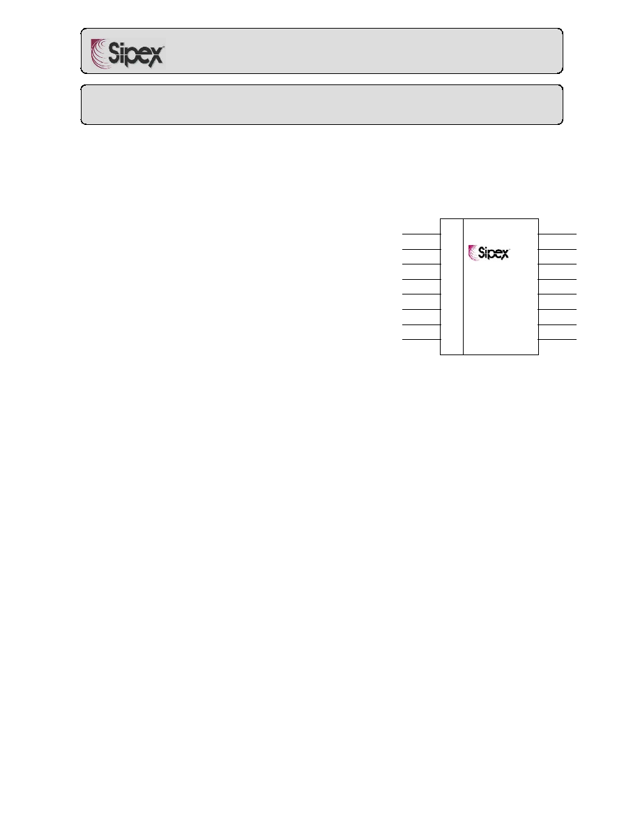
IR
I2
I3
RF
EN2
EN3
ENABLE
OSCEN
Vcc
Iout A
GND
RSA
RSB
Iout B
SELA
Vcc
SP8107
SSOP-16
FEATURES
∑ Three current controlled inputs with independent
ENABLE/DISABLE
∑ Two selectable outputs for grounded laser diodes
∑ Output current up to 400mA (250mA per input channel)
∑ Independent swing for each output channel controlled
by external resistor
∑ On-chip oscillator with resistor controlled frequency
∑ Single 5V power supply
∑ Common ENABLE and oscillator ENABLE inputs
∑ TTL/CMOS logic level control signals
∑ Small SSOP16 package
APPLICATION
∑ DVD-RAM with CD-RW capability
∑ DVD-RW with CD-RW capability
∑ Writable data storage optical devices
GENERAL DESCRIPTION
The SP8107 is a three channel laser diode driver specifically designed for high speed DVD-RW or DVD-
RAM applications. It operates two grounded laser diodes (650nm for DVD and 780nm for CD) and
features three input channels that allow setting of three different optical power levels. The first channel
(IR) has lower gain (100mA/mA) and output current (up to 200mA) and is used as a read channel. The
second (I2) and third (I3) channels have higher gain (250mA/mA) and output current (up to 250mA) and
are used as write channels. Each write channel may be switched on/off at very fast switching speeds with
TTL/CMOS logic level signals applied to EN2 and EN3 inputs - channels are enabled at low logic level
and disabled at high logic level. Outputs of all channels are summed together and connected to one of the
outputs I
OUT
A or I
OUT
B depending on logic signal at the input SELA. High logic level at SELA selects
output I
OUT
A, while low logic level selects output I
OUT
B. Inputs IR, I2, and I3 are current-controlled with
200 ohm DC impedance but allow voltage control by using external limiting resistors.
An on-chip oscillator is used to reduce laser mode hopping in read mode. The frequency of this oscillator
may be changed by an external resistor connected to the RF pin. Oscillator swing can be set separately for
I
OUT
A and I
OUT
B outputs by two resistors connected to RSA and RSB pins respectively. The oscillator is
enabled by high logic level at the OSCEN pin.
Low logic level at the ENABLE pin disables the entire device. Supply current in disabled mode is below
100uA. Pins EN2 and EN3 have internal pull-up resistors. Pins ENABLE, OSCEN, and SELA have
internal pull-down resistors.
Three Channel High Performance Laser Driver
Advanced
SP8107
Rev. 09/05/03 SP8107 ≠ Three Channel Laser Driver
Copyright 2003 Sipex Corporation
SIPEX RESERVES THE RIGHT TO MAKE CHANGES TO THIS DATASHEET. CALL FOR UPDATES: 1-978-667-8700.
SIPEX CONFIDENTIAL, ADVANCED & PROPRIETARY. DO NOT DISTRIBUTE OR
COPY
page
2
of
3
PIN ASSIGNMENTS
Pin
Number
Pin
Name
Pin Function
1
IR
Read Channel current controlled input
2
I2
Write Channel 2 current controlled input
3
I3
Write Channel 3 current controlled input
4
RF
Connection of an external resistor to GND to set oscillator frequency
5
EN2
Write Channel 2 enable input with an internal pull-up resistor. Logic high or
floating turns channel off.
6
EN3
Write Channel 3 enable input with an internal pull-up resistor. Logic high or
floating turns channel off.
7
ENABLE Common device enable input with pull-down resistor. Logic low or floating
turns device off.
8
OSCEN
Oscillator enable input with pull-down resistor. Logic low or floating turns
oscillator off.
9
Vcc
Supply voltage. Bypass to GND with 0.1uF ceramic capacitor
10
SELA
Output select input with pull-down resistor. Logic high selects output A, low or
floating selects output B
11 I
OUT
B
Output current source B for a laser diode
12
RSB
Connection of an external resistor to GND to set oscillator swing at the output B
13
RSA
Connection of an external resistor to GND to set oscillator swing at the output A
14 GND Ground
pin
15 I
OUT
A
Output current source A for a laser diode
16
Vcc
Supply voltage. Bypass to GND with ceramic capacitors 0.1 and 0.01uF in
parallel
BOARD LAYOUT AND GROUNDING
To obtain the best performance from the SP8107, a printed circuit board with ground plane is required.
Layout should ensure that analog signal lines (IR, I2, and I3) are separated as much as possible from
digital and output power lines. Output power lines should be as short and wide as possible. High quality,
low series resistance ceramic 0.1 and 0.01uF bypass capacitors should be used at the Vcc pins 9 and 16.
These capacitors must be located as close to the pins as possible. The traces connecting the pins and the
bypassing capacitors must be kept short and should be made as wide as possible.

Advanced
SP8107
Rev. 09/05/03 SP8107 ≠ Three Channel Laser Driver
Copyright 2003 Sipex Corporation
SIPEX RESERVES THE RIGHT TO MAKE CHANGES TO THIS DATASHEET. CALL FOR UPDATES: 1-978-667-8700.
SIPEX CONFIDENTIAL, ADVANCED & PROPRIETARY. DO NOT DISTRIBUTE OR
COPY
page
3
of
3
ORDERING INFORMATION
Part number
Temperature range
Package Type
SP8107
-40 to +85
0
C 16-pin
SSOP